


Motorola MPC2002SG50, MPC2002SG60, MPC2002SG66, MPC2003SG50, MPC2003SG60 Datasheet
...MOTOROLA
SEMICONDUCTOR TECHNICAL DATA
Order this document by MPC2002/D
256KB and 512KB BurstRAM
Secondary Cache Module for PowerPC ± Based Systems
The MPC2002SG and MPC2003SG are designed to provide a burstable, high performance, 256K/512K L2 cache for the PowerPC 60x processors. The modules are configured as 32K x 72 and 64K x 72 bits in a 136 pin dual readout single inline memory module (DIMM). The module uses four of Motorola's MCM67M518 or MCM67M618 BiCMOS BurstRAMs.
Bursts can be initiated with either transfer start processor (TSP) or transfer start controller (TSC). Subsequent burst addresses are generated internal to the BurstRAM by the burst address advance (BAA) pin.
Write cycles are internally self timed and are initiated by the rising edge of the clock (K) input. Eight write enables are provided for byte write control.
The cache family is designed to interface with the PowerPC 60x bus and requires external tag.
PD0 ± PD2 are reserved for density and speed identification.
•PowerPC±style Burst Counter on Board
•Dual Readout SIMM for Circuit Density
•Single 5 V ± 5% Power Supply
•All Inputs and Outputs are TTL Compatible
•Three State Outputs
•Byte Parity
•Byte Write Capability
•Fast Module Clock Rates: 66 MHz, 60 MHz, 50MHz
•Decoupling Capacitors for each Fast Static RAM
•High Quality Multi±Layer FR4 PWB With Separate Power and Ground Planes
•I/Os are 3.3 V Compatible
MPC2002
MPC2003
(Formerly MCM72MS32/64)
136±LEAD DIMM CASE 1104±01 TOP VIEW
1
34 

35 
68
BurstRAM is a trademark of Motorola.
PowerPC and PowerPC 601 are trademarks of International Business Machines Corp.
5/95
Motorola, Inc. 1995

PIN ASSIGNMENT 136±LEAD DIMM CASE 1104±01 TOP VIEW
|
|
|
Cache |
|
PD2 |
PD1 |
PD0 |
Size |
Module |
|
|
|
|
|
VSS |
NC |
NC |
512KB |
MPC2003SG66/60 |
VSS |
NC |
VSS |
512KB |
MPC2003SG50 |
VSS |
VSS |
NC |
256KB |
MPC2002SG66/60 |
VSS |
VSS |
VSS |
256KB |
MPC2002SG50 |
|
|
|
|
|
|
|
|
|
|
|
|
|
|
PIN NAMES |
|
|
|
||||||||||||
|
A0 ± A15 . . . . . . . |
. . . . . . . . . . . . . . . Address Inputs |
||||||||||||
|
K0, K1 . . . . . . . . . . |
. . . . . . . . . . . . . . . . . . . . . . Clock |
||||||||||||
|
|
|
|
± |
|
|
|
|
Byte Write |
|||||
|
W0 |
W7 |
||||||||||||
|
E0, |
|
|
E1 |
|
. . . . . . . . . . |
. . . . . . . . . . . . . . Module Enable |
|||||||
|
G0 |
, |
G1 |
. . . . . . . . . . |
. . . . . . . Module Output Enable |
|||||||||
|
DQ0 ± DQ63 . . . . . |
. . . . . Cache Data Input/Output |
||||||||||||
|
DQP0 ± DQP7 . . . |
. . . . . . Data Parity Input/Output |
||||||||||||
|
|
|
|
|
Transfer Start Controller |
|||||||||
|
TSC |
|||||||||||||
|
TSP |
|
. . . . . . . . . . . . |
. . . . . Transfer Start Processor |
||||||||||
|
BAA |
. . . . . . . . . . . . |
. . . . . . Burst Address Advance |
|||||||||||
|
PD0 ± PD2 . . . . . . |
. . . . . . . . . . . . Presence Detect |
||||||||||||
|
VCC . . . . . . . . . . . . |
. . . . . . . . . . + 5 V Power Supply |
||||||||||||
|
VSS . . . . . . . . . . . . |
. . . . . . . . . . . . . . . . . . . . Ground |
||||||||||||
* This pin on the MPC2002 is a No Connect (NC)
|
PD0 |
1 |
69 |
|
VSS |
|||||||||
|
PD1 |
2 |
70 |
|
PD2 |
|||||||||
DQ0 |
3 |
71 |
|
VCC |
||||||||||
DQ1 |
4 |
72 |
|
DQ2 |
||||||||||
VCC |
5 |
73 |
|
DQ3 |
||||||||||
DQ4 |
6 |
74 |
|
DQ5 |
||||||||||
DQ6 |
7 |
75 |
|
DQ7 |
||||||||||
DQP0 |
8 |
76 |
|
VSS |
||||||||||
DQ8 |
9 |
77 |
|
DQ9 |
||||||||||
DQ10 |
10 |
78 |
|
DQ11 |
||||||||||
|
VSS |
11 |
79 |
|
DQ12 |
|||||||||
|
|
K0 |
12 |
80 |
|
VSS |
||||||||
|
VSS |
13 |
81 |
|
DQ13 |
|||||||||
DQ14 |
14 |
82 |
|
DQ15 |
||||||||||
VCC |
15 |
83 |
|
DQP1 |
||||||||||
DQ16 |
16 |
84 |
|
VSS |
||||||||||
DQ17 |
17 |
85 |
|
DQ18 |
||||||||||
DQ19 |
18 |
86 |
|
DQ20 |
||||||||||
DQ21 |
19 |
87 |
|
DQ22 |
||||||||||
VCC |
20 |
88 |
|
DQ23 |
||||||||||
DQP2 |
21 |
89 |
|
VSS |
||||||||||
DQ24 |
22 |
90 |
|
DQ25 |
||||||||||
DQ26 |
23 |
91 |
|
DQ27 |
||||||||||
DQ28 |
24 |
92 |
|
DQ29 |
||||||||||
|
VSS |
25 |
93 |
|
DQ30 |
|||||||||
DQ31 |
26 |
94 |
|
VSS |
||||||||||
DQP3 |
27 |
95 |
|
|
|
|
|
|
||||||
|
E0 |
|||||||||||||
|
VSS |
28 |
96 |
|
W1 |
|
|
|
||||||
|
|
W0 |
29 |
97 |
|
|
|
|
|
|||||
|
|
|
W3 |
|||||||||||
|
|
|
|
|
30 |
98 |
|
|
|
|
||||
|
|
W2 |
|
|
|
G0 |
||||||||
|
|
|
31 |
99 |
|
|
|
|||||||
|
TSP |
|
|
TSC |
||||||||||
|
|
|
32 |
100 |
|
VSS |
||||||||
|
BAA |
|
||||||||||||
VCC |
33 |
101 |
|
G1 |
|
|||||||||
|
|
W4 |
34 |
102 |
|
W5 |
|
|||||||
|
|
|
|
|
35 |
103 |
|
|
|
|
|
|
|
|
|
|
W6 |
W7 |
|||||||||||
DQ32 |
36 |
104 |
|
E1 |
|
|
|
|
||||||
DQ33 |
37 |
105 |
|
DQ34 |
||||||||||
|
VSS |
38 |
106 |
|
DQ35 |
|||||||||
DQ36 |
39 |
107 |
|
DQ37 |
||||||||||
DQ38 |
40 |
108 |
|
VCC |
||||||||||
DQ39 |
41 |
109 |
|
DQP4 |
||||||||||
DQ40 |
42 |
110 |
|
DQ41 |
||||||||||
VCC |
|
43 |
111 |
|
DQ42 |
|||||||||
|
||||||||||||||
DQ43 |
|
44 |
112 |
|
DQ44 |
|||||||||
DQ45 |
|
45 |
113 |
|
VSS |
|||||||||
DQ46 |
|
46 |
114 |
|
DQ47 |
|||||||||
DQP5 |
|
47 |
115 |
|
DQ48 |
|||||||||
|
VSS |
|
48 |
116 |
|
DQ49 |
||||||||
|
|
K1 |
|
49 |
117 |
|
VSS |
|||||||
|
VSS |
|
50 |
118 |
|
DQ50 |
||||||||
DQ52 |
|
51 |
119 |
|
DQ51 |
|||||||||
DQ53 |
|
52 |
120 |
|
DQ54 |
|||||||||
DQ55 |
|
53 |
121 |
|
DQ56 |
|||||||||
DQP6 |
|
54 |
122 |
|
VSS |
|||||||||
VCC |
|
55 |
123 |
|
DQ57 |
|||||||||
DQ58 |
|
56 |
124 |
|
DQ59 |
|||||||||
DQ60 |
|
57 |
125 |
|
DQ61 |
|||||||||
DQ62 |
|
58 |
126 |
|
DQ63 |
|||||||||
DQP7 |
|
59 |
127 |
|
VCC |
|||||||||
|
|
A0 |
|
60 |
128 |
|
A1 |
|||||||
|
|
A2 |
|
61 |
129 |
|
A3 |
|||||||
|
|
A4 |
|
62 |
130 |
|
A5 |
|||||||
|
|
A6 |
|
63 |
131 |
|
A7 |
|||||||
|
|
A8 |
|
64 |
132 |
|
NC |
|||||||
|
A10 |
|
65 |
133 |
|
A9 |
||||||||
|
A12 |
|
66 |
134 |
|
A11 |
||||||||
|
A14 |
|
67 |
135 |
|
A13 |
||||||||
|
VSS |
|
68 |
136 |
|
A15* |
||||||||
|
|
|
|
|
|
|
|
|
|
|
|
|
|
|
MPC2002•MPC2003 |
MOTOROLA FAST SRAM |
2 |
|

|
|
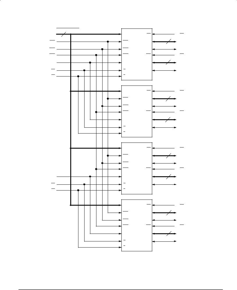
MPC2003 (64K x 72) MODULE BLOCK DIAGRAM |
|
|
16 |
MCM67M618 |
|
A0 ± A15 |
|
||
|
A0 ± A15 |
LW |
|
|
|
||
|
|
|
8 |
TSP |
|
TSP |
DQ0 ± DQ7 |
TSC |
|
TSC |
DQ8 |
BAA |
|
BAA |
UW |
|
|
|
8 |
K0 |
|
K |
DQ9 ± DQ16 |
G0 |
|
G |
DQ17 |
E0 |
|
E |
|
|
|
MCM67M618 |
|
|
|
A0 ± A15 |
LW |
|
|
|
8 |
|
|
TSP |
DQ0 ± DQ7 |
|
|
TSC |
DQ8 |
|
|
BAA |
UW |
|
|
|
8 |
|
|
K |
DQ9 ± DQ16 |
|
|
G |
DQ17 |
|
|
E |
|
|
|
MCM67M618 |
|
|
|
A0 ± A15 |
LW |
|
|
|
8 |
|
|
TSP |
DQ0 ± DQ7 |
|
|
TSC |
DQ8 |
|
|
BAA |
UW |
K1 |
|
|
8 |
|
K |
DQ9 ± DQ16 |
|
G1 |
|
G |
DQ17 |
E1 |
|
E |
|
|
|
MCM67M618 |
|
|
|
A0 ± A15 |
LW |
|
|
|
8 |
|
|
TSP |
DQ0 ± DQ7 |
|
|
TSC |
DQ8 |
|
|
BAA |
UW |
|
|
|
8 |
|
|
K |
DQ9 ± DQ16 |
|
|
G |
DQ17 |
|
|
E |
|
W0
DQ0 ± DQ7
DQP0
W1
DQ8 ± DQ15
DQP1
W2
DQ16 ± DQ23 DQP2
W3
DQ24 ± DQ31
DQP3
W4
DQ32 ± DQ39 DQP4
W5
DQ40 ± DQ47
DQP5
W6
DQ48 ± DQ55 DQP6
W7
DQ56 ± DQ63
DQP7
MOTOROLA FAST SRAM |
MPC2002•MPC2003 |
|
3 |
|
MPC2002 (32K x 72) MODULE BLOCK DIAGRAM |
|
|
A15 |
NC |
|
|
15 |
MCM67M518 |
|
|
A0 ± A14 |
A0 ± A14 |
LW |
W0 |
|
|||
|
|
|
8 |
TSP |
TSP |
DQ0 ± DQ7 |
DQ0 ± DQ7 |
TSC |
TSC |
DQ8 |
DQP0 |
BAA |
BAA |
UW |
W1 |
K0 |
K |
DQ9 ± DQ16 |
8 |
DQ8 ± DQ15 |
|||
G0 |
G |
DQ17 |
DQP1 |
E0 |
E |
|
|
|
MCM67M518 |
|
|
|
A0 ± A14 |
LW |
W2 |
|
|
|
8 |
|
TSP |
DQ0 ± DQ7 |
DQ16 ± DQ23 |
|
TSC |
DQ8 |
DQP2 |
|
BAA |
UW |
W3 |
|
|
|
8 |
|
K |
DQ9 ± DQ16 |
DQ24 ± DQ31 |
|
G |
DQ17 |
DQP3 |
|
E |
|
|
|
MCM67M518 |
|
|
|
A0 ± A14 |
LW |
W4 |
|
|
|
8 |
|
TSP |
DQ0 ± DQ7 |
DQ32 ± DQ39 |
|
TSC |
DQ8 |
DQP4 |
|
BAA |
UW |
W5 |
|
|
|
8 |
K1 |
K |
DQ9 ± DQ16 |
DQ40 ± DQ47 |
G1 |
G |
DQ17 |
DQP5 |
E1 |
E |
|
|
|
MCM67M518 |
|
|
|
A0 ± A14 |
LW |
W6 |
|
|
|
8 |
|
TSP |
DQ0 ± DQ7 |
DQ48 ± DQ55 |
|
TSC |
DQ8 |
DQP6 |
|
BAA |
UW |
W7 |
|
K |
DQ9 ± DQ16 |
8 |
|
DQ56 ± DQ63 |
||
|
G |
DQ17 |
DQP7 |
|
E |
|
|
MPC2002•MPC2003 |
|
|
MOTOROLA FAST SRAM |
4 |
|
|
|
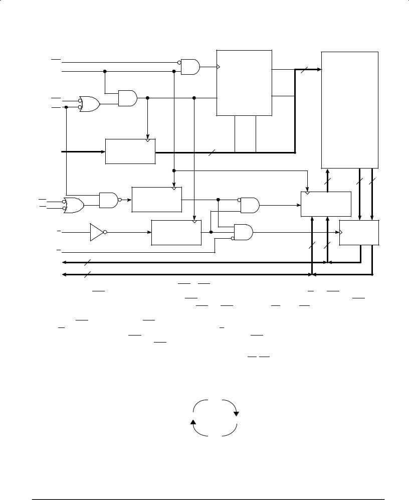
BLOCK DIAGRAM (See Note)
BURST LOGIC
|
|
|
|
|
INTERNAL |
|
|
|
BAA |
|
|
|
A1′ |
ADDRESS |
|
|
|
K |
|
|
Q1 |
|
|
|
|
|
|
|
|
|
|
|
|
||
|
BINARY |
|
|
16 |
|
|
|
|
|
|
|
|
|
|
|
||
|
|
COUNTER |
|
|
|
|
|
|
|
|
|
Q0 |
A0′ |
|
|
|
|
TSC |
LOAD |
|
|
|
|
|
|
|
|
|
|
|
|
64K x 18 |
|
||
TSP |
|
D1 |
D0 |
|
|
|
MEMORY |
|
|
|
|
|
ARRAY |
|
|||
|
|
|
|
|
|
|||
|
|
|
|
|
|
|
|
|
|
A1 |
A0 |
|
|
|
|
|
|
EXTERNAL |
|
|
|
|
|
|
|
|
ADDRESS |
ADDRESS |
|
|
A15 ± A2 |
|
|
|
|
A15 ± A0 |
REGISTERS |
|
|
|
|
|
|
|
|
16 |
|
|
|
|
|
|
|
|
|
|
|
|
|
18 |
9 |
9 |
|
WRITE |
|
|
|
|
DATA±IN |
|
|
UW |
REGISTER |
|
|
|
|
|
|
|
LW |
|
|
|
|
|
REGISTERS |
|
|
|
|
|
|
|
|
|
|
|
E |
ENABLE |
|
|
|
|
|
OUTPUT |
|
REGISTER |
|
|
|
|
|
BUFFER |
||
|
|
|
|
|
|
|||
|
|
|
|
|
9 |
9 |
|
|
G |
|
|
|
|
|
|
|
|
9 |
|
|
|
|
|
|
|
|
DQ0 ± DQ8 |
|
|
|
|
|
|
|
|
9
DQ9 ± DQ17
NOTE: All registers are positive±edge triggered. The TSC or TSP signals control the duration of the burst and the start of the next burst. When TSP is sampled low, any ongoing burst is interrupted and a read (independent of W and TSC) is performed using the new external address. Alternatively, a TSP±initiated two cycle WRITE can be performed by asserting TSP and a valid address on the first cycle, then negating both TSP and TSC and asserting LW and/or UW with valid data on the second cycle (see Single Write Cycle in WRITE CYCLES timing diagram).
When TSC is sampled low (and TSP is sampled high), any ongoing burst is interrupted and a read or write (dependent on W) is performed using the new external address. Chip enable (E) is sampled only when a new base address is loaded. After the first cycle of the burst, BAA controls subsequent burst cycles. When BAA is sampled low, the internal address is advanced prior to the operation. When BAA is sampled high, the internal address is not advanced, thus inserting a wait state into the burst sequence accesses. Upon completion of a burst, the address will wrap around to its initial state. See BURST SEQUENCE GRAPH. Write refers to either or both byte write enables (LW, UW).
BURST SEQUENCE GRAPH (See Note)
 0,0
0,0
A1′, A0′= 1,1
0,1
1,0
NOTE: The external two values for A1 and A0 provide the starting point for the burst sequence graph. The burst logic advances A1 and A0 as shown above.
MOTOROLA FAST SRAM |
MPC2002•MPC2003 |
|
5 |
 Loading...