


Order this document by MPX5700/D
MPX5700
SERIES
INTEGRATED
PRESSURE SENSOR
0 to 700 kPa (0 to 101.5 psi)
0.2 to 4.7 V OUTPUT
• Ideally Suited for Microprocessor or Microcontroller±Based Systems |
BASIC CHIP |
||
• |
Available in Differential and Gauge Configurations |
||
CARRIER ELEMENT |
|||
• |
Patented Silicon Shear Stress Strain Gauge |
||
CASE 867±08, STYLE 1 |
|||
• Durable Epoxy Unibody Element |
|
||
|
VS |
|
|
|
|
|
3 |
|
|
|
|
|
THIN FILM |
GAIN STAGE #2 |
|
|
|
X±ducer |
TEMPERATURE |
AND |
1 |
|
|
SENSING |
COMPENSATION |
GROUND |
V |
DIFFERENTIAL |
|
ELEMENT |
AND |
REFERENCE |
|
out |
|
|
|
PORT OPTION |
|||
|
GAIN STAGE #1 |
SHIFT CIRCUITRY |
|
|
|
|
|
|
CASE 867C±05, STYLE 1 |
||
|
|
|
|
|
2 |
PINS 4, 5 AND 6 ARE NO CONNECTS |
|
GND |
|
|
|
|
|
PIN NUMBER |
|
|||
|
|
|
|
|
|
|
|
|
||
Figure 1. Fully Integrated Pressure Sensor Schematic |
|
|
1 |
Vout |
4 |
|
N/C |
|||
|
|
2 |
Gnd |
5 |
|
N/C |
||||
|
|
|
|
|
|
|||||
|
|
|
|
|
|
|
|
|
|
|
|
|
|
|
|
3 |
VS |
6 |
|
N/C |
|
MAXIMUM RATINGS(1) |
|
|
|
|
NOTE: Pins 4, 5, and 6 are internal |
|||||
|
|
|
|
|
device connections. Do not connect |
|||||
Parametrics |
Symbol |
Value |
Unit |
|||||||
|
to external circuitry or ground. Pin 1 |
|||||||||
|
|
|
|
|
||||||
Overpressure (P2 v 1 Atmosphere) |
P1max |
2800 |
kPa |
|
is noted by the notch in the Lead. |
|||||
Burst Pressure (P2 v 1 Atmosphere) |
P1burst |
5000 |
kPa |
|
|
|
|
|
|
|
Storage Temperature |
Tstg |
± 40 to +125 |
°C |
|
|
|
|
|
|
|
Operating Temperature |
TA |
± 40 to +125 |
°C |
|
|
|
|
|
|
|
1.TC = 25°C unless otherwise noted. Maximum Ratings apply to Case 867±08 only.
2.Extended exposure at the specified limits may cause permanent damage or degradation to the device.
3.This sensor is designed for applications where P1 is always greater than, or equal to P2.
Senseon and X±ducer are trademarks of Motorola, Inc.
REV 2
Motorola Sensor Device Data |
1 |
Motorola, Inc. 1997 |
|

MPX5700 SERIES
OPERATING CHARACTERISTICS (VS = 5.0 Vdc, TA = 25°C unless otherwise noted, P1 > P2)
|
Characteristic |
Symbol |
Min |
Typ |
Max |
Unit |
|
|
|
|
|
|
|
Pressure Range(1) |
|
P |
0 |
Ð |
700 |
kPa |
|
|
OP |
|
|
|
|
Supply Voltage(2) |
|
VS |
4.75 |
5.0 |
5.25 |
Vdc |
Supply Current |
|
Io |
± |
7.0 |
10 |
mAdc |
Zero Pressure Offset(3) |
(0 to 85°C) |
V |
0.088 |
0.2 |
0.313 |
Vdc |
|
|
off |
|
|
|
|
Full Scale Output(4) |
(0 to 85°C) |
V |
4.587 |
4.7 |
4.813 |
Vdc |
|
|
FSO |
|
|
|
|
Full Scale Span(5) |
(0 to 85°C) |
V |
Ð |
4.5 |
Ð |
Vdc |
|
|
FSS |
|
|
|
|
Accuracy(6) |
(0 to 85°C) |
Ð |
Ð |
Ð |
± 2.5 |
%V |
|
|
|
|
|
|
FSS |
Sensitivity |
|
V/P |
Ð |
6.4 |
Ð |
mV/kPa |
|
|
|
|
|
|
|
Response Time(7) |
|
tR |
Ð |
1.0 |
Ð |
ms |
Output Source Current at Full Scale Output |
IO+ |
Ð |
0.1 |
Ð |
mAdc |
|
Warm±Up Time(8) |
|
Ð |
Ð |
20 |
Ð |
ms |
Decoupling circuit shown in Figure 4 required to meet electrical specifications.
MECHANICAL CHARACTERISTICS
Characteristic |
Symbol |
Min |
Typ |
Max |
Unit |
|
|
|
|
|
|
Weight, Basic Element (Case 867) |
Ð |
Ð |
4.0 |
Ð |
Grams |
|
|
|
|
|
|
Cavity Volume |
Ð |
Ð |
Ð |
0.01 |
IN3 |
Volumetric Displacement |
Ð |
Ð |
Ð |
0.001 |
IN3 |
NOTES: |
|
|
|
|
|
1.1.0 kPa (kiloPascal) equals 0.145 psi.
2.Device is ratiometric within this specified excitation range.
3.Offset (Voff) is defined as the output voltage at the minimum rated pressure.
4.Full Scale Output (VFSO) is defined as the output voltage at the maximum or full rated pressure.
5.Full Scale Span (VFSS) is defined as the algebraic difference between the output voltage at full rated pressure and the output voltage at the minimum rated pressure.
6.Accuracy (error budget) consists of the following:
• |
Linearity: |
Output deviation from a straight line relationship with pressure over the specified pressure range. |
• |
Temperature Hysteresis: |
Output deviation at any temperature within the operating temperature range, after the temperature is |
|
|
cycled to and from the minimum or maximum operating temperature points, with zero differential pressure |
|
|
applied. |
• |
Pressure Hysteresis: |
Output deviation at any pressure within the specified range, when this pressure is cycled to and from the |
|
|
minimum or maximum rated pressure, at 25°C. |
• |
TcSpan: |
Output deviation over the temperature range of 0° to 85°C, relative to 25°C. |
• |
TcOffset: |
Output deviation with minimum rated pressure applied, over the temperature range of 0° to 85°C, relative |
|
|
to 25°C. |
•Variation from Nominal: The variation from nominal values, for Offset or Full Scale Span, as a percent of VFSS, at 25°C.
7.Response Time is defined as the time for the incremental change in the output to go from 10% to 90% of its final value when subjected to a specified step change in pressure.
8.Warm±up is defined as the time required for the device to meet the specified output voltage after the pressure has been stabilized.
9.P2 max is 500 kPa.
2 |
Motorola Sensor Device Data |
MPX5700 SERIES
ON±CHIP TEMPERATURE COMPENSATION, CALIBRATION AND SIGNAL CONDITIONING
Figure 3 illustrates both the Differential/Gauge and the Absolute Sensing Chip in the basic chip carrier (Case 867). A fluorosilicone gel isolates the die surface and wire bonds from the environment, while allowing the pressure signal to be transmitted to the sensor diaphragm. (For use of the MPX5700D in a high pressure, cyclic application, consult the factory.)
The MPX5700 series pressure sensor operating characteristics, and internal reliability and qualification tests are based on use of dry air as the pressure media. Media, other than dry air, may have adverse effects on sensor performance and
long±term reliability. Contact the factory for information regarding media compatibility in your application.
Figure 4 shows a typical decoupling circuit for interfacing the sensor to the A/D input of a microprocessor. Proper decoupling of the power supply is recommended.
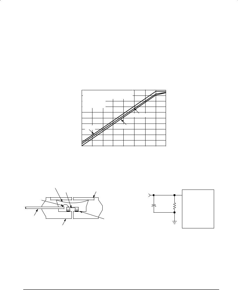
Figure 2 shows the sensor output signal relative to pressure input. Typical, minimum, and maximum output curves are shown for operation over a temperature range of 0° to 85°C using the decoupling circuit below. (The output will saturate outside of the specified pressure range.)
|
5.0 |
TRANSFER FUNCTION: |
|
|
|
|
|
|||
|
4.5 |
|
|
|
|
|
||||
|
V |
= V |
*(0.0012858*P+0.04) |
± ERROR |
|
|
|
|
||
|
4.0 |
out |
S |
|
|
|
|
|
|
|
|
VS = 5.0 Vdc |
|
|
|
|
|
|
|||
(V) |
3.5 |
TEMP = 0 to 85°C |
|
|
|
|
|
|
||
3.0 |
|
|
|
|
|
|
|
|
|
|
OUTPUT |
|
|
|
|
|
TYPICAL |
|
|
||
2.5 |
|
|
|
|
|
|
|
|||
|
|
|
|
|
|
|
|
|
||
2.0 |
|
|
|
|
|
|
|
|
|
|
|
|
|
|
|
MIN |
|
|
|
|
|
|
1.5 |
MAX |
|
|
|
|
|
|
||
|
|
|
|
|
|
|
|
|
|
|
|
1.0 |
|
|
|
|
|
|
|
|
|
|
0.5 |
|
|
|
|
|
|
|
|
|
|
0 |
|
100 |
200 |
300 |
400 |
500 |
600 |
700 |
800 |
|
0 |
|
||||||||
|
|
|
|
DIFFERENTIAL PRESSURE (kPa) |
|
|
||||
Figure 2. Output versus Pressure Differential
|
FLUORO SILICONE |
|
|
|
|
|
DIE COAT |
STAINLESS STEEL |
|
|
|
|
DIE |
METAL COVER |
MPX5700 |
|
|
|
P1 |
|
|
A/D |
|
|
|
OUTPUT |
|
||
WIRE BOND |
|
|
(PIN 1) |
|
|
|
|
|
50 pF |
51 k |
μ PROCESSOR |
|
|
|
|
|
|
LEAD |
|
RTV DIE |
|
|
|
FRAME |
P2 |
BOND |
|
|
|
|
|
|
|
|
|
|
EPOXY CASE |
|
|
|
|
Figure 3. Cross±Sectional Diagram |
Figure 4. Typical Decoupling Filter for Sensor to |
(Not to Scale) |
Microprocessor Interface |
Motorola Sensor Device Data |
3 |
 Loading...