


MOTOROLA MPS2907ARLRM, MPS2907ARLRP, MPS2907AZL1, MPS2907ARL, MPS2907ARL1 Datasheet
...
MOTOROLA
SEMICONDUCTOR TECHNICAL DATA
Order this document by MPS2907/D
General Purpose Transistors
PNP Silicon
|
|
|
|
|
COLLECTOR |
||||
|
|
|
3 |
|
|
||||
|
|
|
2 |
|
|
|
|
|
|
|
|
|
|
|
|
|
|
||
|
|
|
|
|
|
|
|
||
|
|
|
BASE |
|
|
|
|
||
|
|
|
|
|
|
||||
|
|
|
1 |
|
|||||
|
|
|
|
|
|
EMITTER |
|||
MAXIMUM RATINGS |
|
|
|
|
|
|
|
|
|
|
|
|
|
|
|
|
|
|
|
Rating |
Symbol |
MPS2907 |
|
MPS2907A |
Unit |
||||
|
|
|
|
|
|
|
|
|
|
Collector± Emitter Voltage |
VCEO |
±40 |
|
±60 |
|
|
|
Vdc |
|
Collector± Base Voltage |
VCBO |
|
±60 |
|
|
|
|
Vdc |
|
Emitter± Base Voltage |
VEBO |
|
±5.0 |
|
|
|
|
Vdc |
|
Collector Current Ð Continuous |
IC |
±600 |
|
|
|
|
mAdc |
||
Total Device Dissipation |
PD |
|
|
|
|
|
|
|
|
@ TA = 25°C |
|
|
625 |
|
|
|
|
mW |
|
Derate above 25°C |
|
|
5.0 |
|
|
|
|
mW/°C |
|
|
|
|
|
|
|
|
|
|
|
Total Device Dissipation |
PD |
|
|
|
|
|
|
|
|
@ TC = 25°C |
|
|
1.5 |
|
|
|
|
Watts |
|
Derate above 25°C |
|
|
12 |
|
|
|
|
mW/°C |
|
|
|
|
|
|
|
|
|
||
Operating and Storage Junction |
TJ, Tstg |
± 500 to +150 |
°C |
||||||
Temperature Range |
|
|
|
|
|
|
|
|
|
|
|
|
|
|
|
|
|
|
|
THERMAL CHARACTERISTICS |
|
|
|
|
|
|
|
|
|
MPS2907 MPS2907A*
*Motorola Preferred Device
1
2 3
CASE 29±04, STYLE 1
TO±92 (TO±226AA)
Characteristic |
Symbol |
|
Max |
Unit |
|
|
|
|
|
|
|
|
|
|
|
|
|
|
|
Thermal Resistance, Junction to Ambient |
RqJA |
|
200 |
°C/W |
|
|
|
|
|
Thermal Resistance, Junction to Case |
RqJC |
|
83.3 |
°C/W |
|
|
|
|
|
ELECTRICAL CHARACTERISTICS (TA = 25°C unless otherwise noted) |
|
|
|
|
|
|
|||
Characteristic |
|
|
|
Symbol |
Min |
Max |
Unit |
||
|
|
|
|
|
|
|
|
|
|
OFF CHARACTERISTICS |
|
|
|
|
|
|
|
|
|
|
|
|
|
|
|
|
|
|
|
Collector± Emitter Breakdown Voltage(1) |
MPS2907 |
|
|
|
V(BR)CEO |
±40 |
Ð |
Vdc |
|
(IC = ±10 mAdc, IB = 0) |
MPS2907A |
|
|
|
|
±60 |
Ð |
|
|
Collector± Base Breakdown Voltage |
|
|
|
|
|
V(BR)CBO |
±60 |
Ð |
Vdc |
(IC = ±10 mAdc, IE = 0) |
|
|
|
|
|
|
|
|
|
Emitter± Base Breakdown Voltage |
|
|
|
|
|
V(BR)EBO |
±5.0 |
Ð |
Vdc |
(IE = ±10 mAdc, IC = 0) |
|
|
|
|
|
|
|
|
|
Collector Cutoff Current |
|
|
|
|
|
ICEX |
Ð |
±50 |
nAdc |
(VCE = ±30 Vdc, VEB(off) = ±0.5 Vdc) |
|
|
|
|
|
|
|
|
|
Collector Cutoff Current |
|
|
|
|
|
ICBO |
|
|
μAdc |
(VCB = ±50 Vdc, IE = 0) |
MPS2907 |
|
|
|
|
Ð |
±0.02 |
|
|
|
MPS2907A |
|
|
|
|
Ð |
±0.01 |
|
|
(VCB = ±50 Vdc, IE = 0, TA = 150°C) |
MPS2907 |
|
|
|
|
Ð |
±20 |
|
|
|
MPS2907A |
|
|
|
|
Ð |
±10 |
|
|
|
|
|
|
|
|
|
|
|
|
Base Current |
|
|
|
|
|
IB |
Ð |
±50 |
nAdc |
(VCE = ±30 Vdc, VEB(off) = ±0.5 Vdc) |
|
|
|
|
|
|
|
|
|
1. Pulse Test: Pulse Width v 300 ms, Duty Cycle v 2.0%. |
|
|
|
|
|
|
|
||
Preferred devices are Motorola recommended choices for future use and best overall value.
Motorola, Inc. 1996
MPS2907 |
MPS2907A |
|
|
|
|
|
|
ELECTRICAL CHARACTERISTICS (TA = 25°C unless otherwise noted) (Continued) |
|
|
|
||||
|
|
|
|
|
|
|
|
|
|
Characteristic |
|
Symbol |
Min |
Max |
Unit |
|
|
|
|
|
|
|
|
ON CHARACTERISTICS |
|
|
|
|
|
||
|
|
|
|
|
|
|
|
DC Current Gain |
|
hFE |
|
|
Ð |
||
(IC = ±0.1 mAdc, VCE = ±10 Vdc) |
MPS2907 |
|
35 |
Ð |
|
||
|
|
|
MPS2907A |
|
75 |
Ð |
|
(IC = ±1.0 mAdc, VCE = ±10 Vdc) |
MPS2907 |
|
50 |
Ð |
|
||
|
|
|
MPS2907A |
|
100 |
Ð |
|
(IC = ±10 mAdc, VCE = ±10 Vdc) |
MPS2907 |
|
75 |
Ð |
|
||
(IC = ±150 mAdc, VCE = ±10 Vdc)(1) |
MPS2907A |
|
100 |
Ð |
|
||
MPS2907, MPS2907A |
|
100 |
300 |
|
|||
(IC = ±500 mAdc, VCE = ±10 Vdc)(1) |
MPS2907 |
|
30 |
Ð |
|
||
|
|
|
MPS2907A |
|
50 |
Ð |
|
|
|
|
|
|
|
|
|
Collector± Emitter Saturation Voltage(1) |
|
VCE(sat) |
Ð |
±0.4 |
Vdc |
||
(IC = ±150 mAdc, IB = ±15 mAdc) |
|
|
|
||||
(IC = ±500 mAdc, IB = ±50 mAdc) |
|
|
Ð |
±1.6 |
|
||
Base ± Emitter Saturation Voltage(1) |
|
VBE(sat) |
Ð |
±1.3 |
Vdc |
||
(IC = ±150 mAdc, IB = ±15 mAdc) |
|
|
|
||||
(IC = ±500 mAdc, IB = ±50 mAdc) |
|
|
Ð |
±2.6 |
|
||
SMALL± SIGNAL CHARACTERISTICS |
|
|
|
|
|
||
|
|
|
|
|
|
|
|
Current± Gain Ð Bandwidth Product (1), (2) |
|
f |
200 |
Ð |
MHz |
||
(IC = ±50 mAdc, VCE = ±20 Vdc, f = 100 MHz) |
|
T |
|
|
|
||
|
|
|
|
|
|||
Output Capacitance |
|
Cobo |
Ð |
8.0 |
pF |
||
(VCB = ±10 Vdc, IE = 0, f = 1.0 MHz) |
|
|
|
|
|
||
Input Capacitance |
|
Cibo |
Ð |
30 |
pF |
||
(VEB = ±2.0 Vdc, IC = 0, f = 1.0 MHz) |
|
|
|
|
|
||
SWITCHING CHARACTERISTICS |
|
|
|
|
|
||
|
|
|
|
|
|
|
|
Turn±On Time |
|
(VCC = ±30 Vdc, IC = ±150 mAdc, |
ton |
Ð |
45 |
ns |
|
|
|
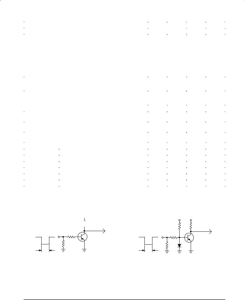
IB1 = ±15 mAdc) (Figures 1 and 5) |
|
|
|
|
|
Delay Time |
|
td |
Ð |
10 |
ns |
||
|
|
|
|||||
Rise Time |
|
|
|
tr |
Ð |
40 |
ns |
Turn±Off Time |
|
(VCC = ±6.0 Vdc, IC = ±150 mAdc, |
toff |
Ð |
100 |
ns |
|
|
|
IB1 = IB2 = 15 mAdc) (Figure 2) |
|
|
|
|
|
Storage Time |
|
ts |
Ð |
80 |
ns |
||
|
|
|
|||||
Fall Time |
|
|
|
tf |
Ð |
30 |
ns |
1.Pulse Test: Pulse Width v 300 ms, Duty Cycle v 2.0%.
2.fT is defined as the frequency at which |hfe| extrapolates to unity.
INPUT
Zo = 50 Ω
PRF = 150 PPS
RISE TIME ≤ 2.0 ns
P.W. < 200 ns
1.0 k
0 |
|
±16 V |
50 |
|
200 ns |
 ±30 V
±30 V  200
200
TO OSCILLOSCOPE RISE TIME ≤ 5.0 ns
INPUT |
|
|
|
|
Zo = 50 Ω |
|
+15 V |
±6.0 V |
|
PRF = 150 PPS |
|
|
|
|
RISE TIME ≤ 2.0 ns |
|
1.0 k |
37 |
|
P.W. < 200 ns |
|
|||
|
|
|
|
|
0 |
1.0 k |
|
TO OSCILLOSCOPE |
|
|
|
|
||
|
|
|
|
RISE TIME ≤ 5.0 ns |
±30 V |
50 |
1N916 |
|
|
200 ns |
|
|
|
|
Figure 1. Delay and Rise Time Test Circuit |
Figure 2. Storage and Fall Time Test Circuit |
2 |
Motorola Small±Signal Transistors, FETs and Diodes Device Data |
 Loading...