


Motorola MPX5010GVP, MPX5010DP, MPX5010GP, MPX5010GS, MPX5010GVS Datasheet
...
MOTOROLA
SEMICONDUCTOR TECHNICAL DATA
Order this document by MPX5010/D
|
MPX5010 |
|
Integrated Silicon Pressure Sensor |
SERIES |
|
On-Chip Signal Conditioned, |
|
|
Temperature Compensated |
INTEGRATED |
|
and Calibrated |
||
PRESSURE SENSOR |
||
The MPX5010 series piezoresistive transducer is a state±of±the±art monolithic silicon |
0 to 10 kPa (0 to 1.45 psi) |
|
0.2 to 4.7 V OUTPUT |
||
pressure sensor designed for a wide range of applications, but particularly those |
|
|
employing a microcontroller or microprocessor with A/D inputs. This patented, single |
|
|
element transducer combines advanced micromachining techniques, thin±film metalliza- |
|
|
tion, and bipolar processing to provide an accurate, high level analog output signal that |
|
|
is proportional to the applied pressure. |
|
|
Features |
|
|
• 5.0% Maximum Error over 0° to 85°C |
|
|
• Ideally Suited for Microprocessor or Microcontroller±Based Systems |
BASIC CHIP |
|
• Patented Silicon Shear Stress Strain Gauge |
||
CARRIER ELEMENT |
||
• Durable Epoxy Unibody Element |
CASE 867±08, STYLE 1 |
|
|
• |
Temperature Compensated over |
40° to +125°C |
|
|
||
|
|
|
VS |
|
|
|
|
|
|
3 |
|
|
|
|
|
|
THIN FILM |
GAIN STAGE #2 |
|
|
|
X±ducer |
TEMPERATURE |
AND |
1 |
|
|
|
SENSING |
COMPENSATION |
GROUND |
V |
||
|
|
|
|
|
|
out |
|
ELEMENT |
|
AND |
REFERENCE |
|
DIFFERENTIAL |
|
|
GAIN STAGE #1 |
SHIFT CIRCUITRY |
|
PORT OPTION |
|
|
|
|
|
|
|
CASE 867C±05, STYLE 1 |
|
|
2 |
PINS 4, 5 AND 6 ARE NO CONNECTS |
|
||
|
|
|
|
|||
GND
Figure 1. Fully Integrated Pressure Sensor Schematic
MAXIMUM RATINGS(1)
Parametrics |
Symbol |
Value |
Unit |
|
|
|
|
Overpressure(2) (P1 > P2) |
Pmax |
75 |
kPa |
Burst Pressure(2) (P1 > P2) |
P |
100 |
kPa |
|
burst |
|
|
Storage Temperature |
Tstg |
± 40 to +125 |
°C |
Operating Temperature |
TA |
± 40 to +125 |
°C |
1.TC = 25°C unless otherwise noted.
2.Exposure beyond the specified limits may cause permanent damage or degradation to the device.
PIN NUMBER
1 |
Vout |
4 |
N/C |
2 |
Gnd |
5 |
N/C |
|
|
|
|
3 |
VS |
6 |
N/C |
NOTE: Pins 4, 5, and 6 are internal device connections. Do not connect to external circuitry or ground. Pin 1 is noted by the notch in the Lead.
Senseon and X±ducer are trademarks of Motorola, Inc.
REV 2
Motorola Sensor Device Data |
1 |
Motorola, Inc. 1997 |
|

MPX5010 SERIES
OPERATING CHARACTERISTICS (VS = 5.0 Vdc, TA = 25°C unless otherwise noted, P1 > P2)
Characteristic |
|
Symbol |
Min |
Typ |
Max |
Unit |
|
|
|
|
|
|
|
Pressure Range(1) |
|
P |
0 |
Ð |
10 |
kPa |
|
|
OP |
|
|
|
|
Supply Voltage(2) |
|
VS |
4.75 |
5.0 |
5.25 |
Vdc |
Supply Current |
|
Io |
Ð |
7.0 |
10 |
mAdc |
Minimum Pressure Offset(3) |
(0 to 85°C) |
V |
0 |
0.2 |
0.425 |
Vdc |
@ VS = 5.0 Volts |
|
off |
|
|
|
|
|
|
|
|
|
|
|
Full Scale Output(4) |
(0 to 85°C) |
VFSO |
4.475 |
4.7 |
4.925 |
Vdc |
@ VS = 5.0 Volts |
|
|
|
|
|
|
Full Scale Span(5) |
(0 to 85°C) |
V |
Ð |
4.5 |
Ð |
Vdc |
@ VS = 5.0 Volts |
|
FSS |
|
|
|
|
|
|
|
|
|
|
|
Accuracy(6) |
(0 to 85°C) |
Ð |
Ð |
Ð |
± 5.0 |
%V |
|
|
|
|
|
|
FSS |
Sensitivity |
|
V/P |
Ð |
450 |
Ð |
mV/kPa |
|
|
|
|
|
|
|
Response Time(7) |
|
tR |
Ð |
1.0 |
Ð |
ms |
Output Source Current at Full Scale Output |
|
IO+ |
Ð |
0.1 |
Ð |
mAdc |
Warm±Up Time(8) |
|
Ð |
Ð |
20 |
Ð |
ms |
Offset Stability(9) |
|
Ð |
Ð |
± 0.5 |
Ð |
%V |
|
|
|
|
|
|
FSS |
MECHANICAL CHARACTERISTICS
Characteristic |
Symbol |
Min |
Typ |
Max |
Unit |
|
|
|
|
|
|
Weight, Basic Element (Case 867) |
Ð |
Ð |
4.0 |
Ð |
Grams |
|
|
|
|
|
|
Common Mode Line Pressure(10) |
Ð |
Ð |
Ð |
690 |
kPa |
NOTES:
1.1.0 kPa (kiloPascal) equals 0.145 psi.
2.Device is ratiometric within this specified excitation range.
3.Offset (Voff) is defined as the output voltage at the minimum rated pressure.
4.Full Scale Output (VFSO) is defined as the output voltage at the maximum or full rated pressure.
5.Full Scale Span (VFSS) is defined as the algebraic difference between the output voltage at full rated pressure and the output voltage at the minimum rated pressure.
6.Accuracy (error budget) consists of the following:
• |
Linearity: |
Output deviation from a straight line relationship with pressure over the specified pressure range. |
• |
Temperature Hysteresis: |
Output deviation at any temperature within the operating temperature range, after the temperature is |
|
|
cycled to and from the minimum or maximum operating temperature points, with zero differential pressure |
|
|
applied. |
• |
Pressure Hysteresis: |
Output deviation at any pressure within the specified range, when this pressure is cycled to and from the |
|
|
minimum or maximum rated pressure, at 25°C. |
• |
TcSpan: |
Output deviation over the temperature range of 0° to 85°C, relative to 25°C. |
• |
TcOffset: |
Output deviation with minimum rated pressure applied, over the temperature range of 0° to 85°C, relative |
|
|
to 25°C. |
•Variation from Nominal: The variation from nominal values, for Offset or Full Scale Span, as a percent of VFSS, at 25°C.
7.Response Time is defined as the time for the incremental change in the output to go from 10% to 90% of its final value when subjected to a specified step change in pressure.
8.Warm±up is defined as the time required for the product to meet the specified output voltage after the Pressure has been stabilized.
9.Offset stability is the product's output deviation when subjected to 1000 hours of Pulsed Pressure, Temperature Cycling with Bias Test.
10.Common mode pressures beyond what is specified may result in leakage at the case±to±lead interface.
2 |
Motorola Sensor Device Data |
MPX5010 SERIES
ON±CHIP TEMPERATURE COMPENSATION, CALIBRATION AND SIGNAL CONDITIONING
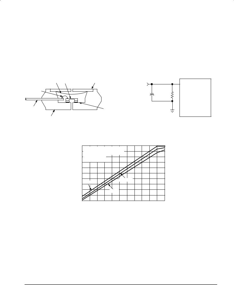
Figure 2 illustrates the Differential/Gauge Sensing Chip in the basic chip carrier (Case 867). A fluorosilicone gel isolates the die surface and wire bonds from the environment, while allowing the pressure signal to be transmitted to the sensor diaphragm.
The MPX5010 series pressure sensor operating characteristics, and internal reliability and qualification tests are based on use of dry air as the pressure media. Media, other than dry air, may have adverse effects on sensor performance and long±term reliability. Contact the factory for information
regarding media compatibility in your application.
Figure 3 shows a typical decoupling circuit for interfacing the integrated sensor to the A/D input of a microprocessor. Proper decoupling of the power supply is recommended.
Figure 4 shows the sensor output signal relative to pressure input. Typical, minimum, and maximum output curves are shown for operation over a temperature range of 0° to 85°C using the decoupling circuit below. (The output will saturate outside of the specified pressure range.)
SILICONE |
DIE |
STAINLESS STEEL |
MPX5010 |
|
|
DIE COAT |
METAL COVER |
|
A/D |
||
|
OUTPUT |
|
|||
|
|
P1 |
(PIN 1) |
|
|
WIRE BOND |
|
|
|
|
|
|
|
50 pF |
|
|
|
|
|
|
51 k |
μ PROCESSOR |
|
|
|
|
|
|
|
LEAD FRAME |
|
RTV DIE |
|
|
|
|
|
BOND |
|
|
|
|
|
P2 |
|
|
|
EPOXY CASE |
|
|
|
|
|
Figure 2. Cross±Sectional Diagram |
Figure 3. Typical Decoupling Filter for Sensor to |
(Not to Scale) |
Microprocessor Interface |
|
5.0 |
TRANSFER FUNCTION: |
|
|
|
|
|
|
|
|
||||
|
4.5 |
|
|
|
|
|
|
|
|
|||||
|
V |
= V |
*(0.09*P+0.04) |
± ERROR |
|
|
|
|
|
|||||
|
|
out |
|
S |
|
|
|
|
|
|
|
|
|
|
|
4.0 |
VS = 5.0 Vdc |
|
|
|
|
|
|
|
|
|
|
||
|
3.5 |
TEMP = 0 to 85°C |
|
|
|
|
|
|
|
|
|
|||
(V) |
|
|
|
|
|
|
|
|
|
|
|
|
|
|
3.0 |
|
|
|
|
|
|
|
|
|
|
|
|
|
|
OUTPUT |
|
|
|
|
|
|
|
|
|
|
|
|
|
|
2.5 |
|
|
|
|
|
|
|
|
|
|
|
|
|
|
|
|
|
|
|
|
|
|
|
|
|
|
|
|
|
|
2.0 |
|
|
|
|
|
|
|
TYPICAL |
|
|
|
|
|
|
|
MAX |
|
|
|
|
|
|
|
|
|
|
||
|
1.5 |
|
|
|
|
|
|
|
|
|
|
|
||
|
|
|
|
|
|
|
|
|
|
|
|
|
|
|
|
1.0 |
|
|
|
|
|
MIN |
|
|
|
|
|
|
|
|
|
|
|
|
|
|
|
|
|
|
|
|
|
|
|
0.5 |
|
|
|
|
|
|
|
|
|
|
|
|
|
|
0 |
|
1 |
2 |
3 |
4 |
5 |
6 |
7 |
8 |
9 |
10 |
11 |
|
|
0 |
|
||||||||||||
|
|
|
|
|
DIFFERENTIAL PRESSURE (kPa) |
|
|
|
||||||
Figure 4. Output versus Pressure Differential
Motorola Sensor Device Data |
3 |
 Loading...