Motorola BD140-10, BD140, BD138, BD136 Datasheet

MOTOROLA
SEMICONDUCTOR TECHNICAL DATA
Order this document by BD136/D
|
|
BD136 |
|
Plastic Medium Power |
Silicon |
BD138 |
|
BD140 |
|||
PNP Transistor |
|
||
|
BD140-10 |
||
|
|
||
. . . designed for use as audio amplifiers and drivers utilizing complementary or quasi |
|
||
complementary circuits. |
|
|
|
• DC Current Gain Ð h FE = 40 (Min) @ IC = 0.15 Adc |
|
1.5 AMPERE |
|
• BD 136, 138, 140 are complementary with BD 135, 137, 139 |
|
POWER TRANSISTORS |
|
|
|
||
|
|
PNP SILICON |
|
|
|
45, 60, 80 VOLTS |
|
|
|
10 WATTS |
|
|
|
|
|
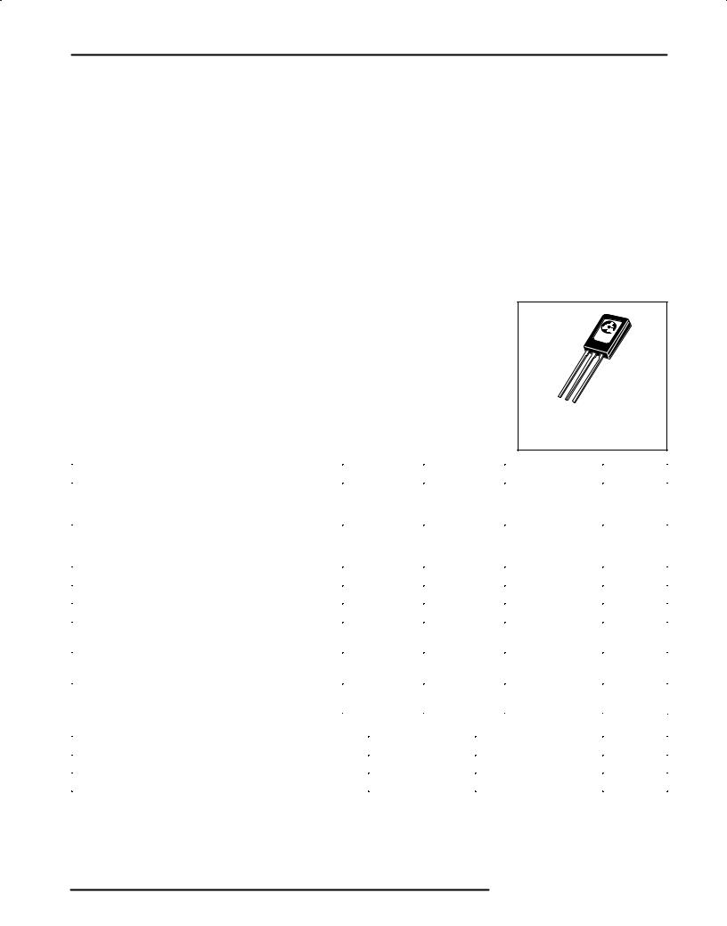
CASE 77±08
TO±225AA TYPE
MAXIMUM RATINGS
Rating |
Symbol |
Type |
Value |
Unit |
|
|
|
|
|
Collector±Emitter Voltage |
VCEO |
BD 136 |
45 |
Vdc |
|
|
BD 138 |
60 |
|
|
|
BD 140 |
80 |
|
|
|
|
|
|
Collector±Base Voltage |
VCBO |
BD 136 |
45 |
Vdc |
|
|
BD 138 |
60 |
|
|
|
BD 140 |
100 |
|
|
|
|
|
|
Emitter±Base Voltage |
VEBO |
|
5 |
Vdc |
Collector Current |
IC |
|
1.5 |
Adc |
Base Current |
IB |
|
0.5 |
Adc |
Total Device Dissipation@ TA = 25_C |
PD |
|
1.25 |
Watts |
Derate above 25_C |
|
|
10 |
mW/_C |
|
|
|
|
|
Total Device Dissipation @ TC = 25_C |
PD |
|
12.5 |
Watt |
Derate above 25_C |
|
|
100 |
mW/_C |
|
|
|
|
|
Operating and Storage Junction |
TJ, Tstg |
|
± 55 to +150 |
_C |
Temperarture Range |
|
|
|
|
|
|
|
|
|
THERMAL CHARACTERISTICS
Characteristic |
Symbol |
Max |
Unit |
|
|
|
|
Thermal Resistance, Junction to Case |
θJC |
10 |
_C/W |
Thermal Resistance, Junction to Ambient |
θJA |
100 |
_C/W |
REV 7
Motorola, Inc. 1995

BD136 BD138 BD140 BD140-10
ELECTRICAL CHARACTERISTICS (TC = 25_C unless otherwise noted)
Characteristic |
|
Symbol |
Type |
Min |
Max |
Unit |
|
|
|
|
|
|
|
Collector±Emitter Sustaining Voltage* |
|
BVCEO |
|
|
|
Vdc |
(IC = 0.03 Adc, IB = 0) |
|
|
BD 136 |
45 |
Ð |
|
|
|
|
BD 138 |
60 |
Ð |
|
|
|
|
BD 140 |
80 |
Ð |
|
|
|
|
|
|
|
|
Collector Cutoff Current |
|
ICBO |
|
|
|
μAdc |
(VCB = 30 Vdc, IE = 0) |
|
|
|
Ð |
0.1 |
|
(VCB = 30 Vdc, IE = 0, TC = 125 _C) |
|
|
|
Ð |
10 |
|
Emitter Cutoff Current |
|
IEBO |
|
Ð |
10 |
μAdc |
(VBE = 5.0 Vdc, IC = 0) |
|
|
|
|
|
|
DC Current Gain |
|
|
|
|
|
Ð |
(IC = 0.005 A, VCE = 2 V) |
ALL |
h * |
|
25 |
Ð |
|
|
|
FE |
|
40 |
250 |
|
|
|
|
|
|
||
(IC = 0.15 A, VCE = 2 V) |
ALL |
|
|
|
|
|
|
BD140±10 |
|
|
63 |
160 |
|
(IC = 0.5 A, VCE = 2 V) |
|
|
|
25 |
Ð |
|
Collector±Emitter Saturation Voltage* |
|
VCE(sat)* |
|
Ð |
0.5 |
Vdc |
(IC = 0.5 Adc, IB = 0.05 Adc) |
|
|
|
|
|
|
Base±Emitter On Voltage* |
|
VBE(on)* |
|
Ð |
1 |
Vdc |
(IC = 0.5 Adc, VCE = 2.0 Vdc) |
|
|
|
|
|
|
* Pulse Test: Pulse Width x 300 μs, Duty Cycle x 2.0%. |
|
|
|
|
|
|
|
10 |
|
|
|
|
|
|
(AMP) |
5.0 |
|
|
|
|
0.1 ms |
|
2.0 |
|
5 ms |
|
|
|
||
|
0.5 ms |
|
|
|
|||
CURRENT |
1.0 |
TJ = 125°C |
|
|
|
|
|
0.5 |
|
dc |
|
|
|
||
|
|
|
|
|
|
||
|
|
|
|
|
|
|
|
COLLECTOR |
0.2 |
|
|
|
|
|
|
0.1 |
|
|
|
|
|
|
|
0.05 |
|
|
|
BD136 |
|
|
|
, |
|
|
|
|
|
|
|
C |
|
|
|
|
|
|
|
I |
0.02 |
|
|
|
BD138 |
|
|
|
|
|
|
|
|
||
|
|
|
|
BD140 |
|
|
|
|
0.01 |
|
|
|
|
|
|
|
2 |
5 |
10 |
20 |
50 |
80 |
|
|
1 |
VCE, COLLECTOR±EMITTER VOLTAGE (VOLTS)
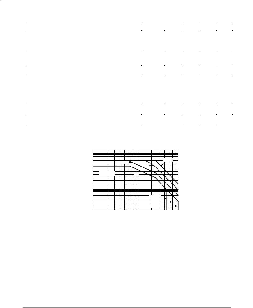
Figure 1. Active±Region Safe Operating Area
2 |
Motorola Bipolar Power Transistor Device Data |
 Loading...