


BUL146F
1
Motorola Bipolar Power Transistor Device Data
SWITCHMODE
NPN Bipolar Power Transistor
For Switching Power Supply Applications
The BUL146/BUL146F have an applications specific state–of–the–art die designed
for use in fluorescent electric lamp ballasts to 130 Watts and in Switchmode Power
supplies for all t ypes of electronic equipment. These h igh voltage/high speed
transistors offer the following:
• Improved Efficiency Due to Low Base Drive Requirements:
— High and Flat DC Current Gain
— Fast Switching
— No Coil Required in Base Circuit for Turn–Off (No Current Tail)
• Full Characterization at 125°C
• Parametric Distributions are Tight and Consistent Lot–to–Lot
• Two Package Choices: Standard TO–220 or Isolated TO–220
• BUL146F, Isolated Case 221D, is UL Recognized to 3500 V
RMS
: File #E69369
MAXIMUM RATINGS
Rating Symbol BUL146 BUL146F Unit
Collector–Emitter Sustaining Voltage V
CEO
400 Vdc
Collector–Emitter Breakdown Voltage V
CES
700 Vdc
Emitter–Base Voltage V
EBO
9.0 Vdc
Collector Current — Continuous
— Peak(1)
I
C
I
CM
6.0
15
Adc
Base Current — Continuous
— Peak(1)
I
B
I
BM
4.0
8.0
Adc
RMS Isolated Voltage(2) Test No. 1 Per Fig. 22a
(for 1 sec, R.H. < 30%, Test No. 2 Per Fig. 22b
T
C
= 25°C) Test No. 3 Per Fig. 22c
V
ISOL
—
—
—
4500
3500
1500
V
Total Device Dissipation (T
C
= 25°C)
Derate above 25°C
P
D
100
0.8
40
0.32
Watts
W/°C
Operating and Storage Temperature T
J
, T
stg
– 65 to 150 °C
THERMAL CHARACTERISTICS
Rating Symbol BUL44 BUL44F Unit
Thermal Resistance — Junction to Case
— Junction to Ambient
R
θJC
R
θJA
1.25
62.5
3.125
62.5
°C/W
Maximum Lead Temperature for Soldering
Purposes: 1/8″ from Case for 5 Seconds
T
L
260 °C
ELECTRICAL CHARACTERISTICS (T
C
= 25°C unless otherwise noted)
Characteristic
Symbol Min Typ Max Unit
OFF CHARACTERISTICS
Collector–Emitter Sustaining Voltage (I
C
= 100 mA, L = 25 mH) V
CEO(sus)
400 — — Vdc
Collector Cutoff Current (V
CE
= Rated V
CEO
, I
B
= 0) I
CEO
— — 100 µAdc
Collector Cutoff Current (V
CE
= Rated V
CES
, V
EB
= 0)
(T
C
= 125°C)
Collector Cutoff Current (V
CE
= 500 V, V
EB
= 0) (T
C
= 125°C)
I
CES
—
—
—
—
—
—
100
500
100
µAdc
Emitter Cutoff Current (V
EB
= 9.0 Vdc, I
C
= 0) I
EBO
— — 100 µAdc
(1) Pulse Test: Pulse Width = 5.0 ms, Duty Cycle ≤ 10%. (continued)
(2) Proper strike and creepage distance must be provided.
Designer’s and SWITCHMODE are trademarks of Motorola, Inc.
Designer’s Data for “Worst Case” Conditions — The Designer’s Data Sheet permits the design of most circuits entirely from the information presented. SOA Limit
curves — representing boundaries on device characteristics — are given to facilitate “worst case” design.
Preferred devices are Motorola recommended choices for future use and best overall value.
MOTOROLA
SEMICONDUCTOR TECHNICAL DATA
Order this document
by BUL146/D
Motorola, Inc. 1995
BUL146
BUL146F
POWER TRANSISTOR
6.0 AMPERES
700 VOLTS
40 and 100 WATTS
*Motorola Preferred Device
BUL146
CASE 221A–06
TO–220AB
BUL146F
CASE 221D–02
ISOLATED TO–220 TYPE
UL RECOGNIZED
*
*
REV 1
2
Motorola Bipolar Power Transistor Device Data
ELECTRICAL CHARACTERISTICS — continued
(T
C
= 25°C unless otherwise noted)
Characteristic
Symbol Min Typ Max Unit
ON CHARACTERISTICS
Base–Emitter Saturation Voltage (I
C
= 1.3 Adc, I
B
= 0.13 Adc)
Base–Emitter Saturation Voltage (I
C
= 3.0 Adc, I
B
= 0.6 Adc)
V
BE(sat)
—
—
0.82
0.93
1.1
1.25
Vdc
Collector–Emitter Saturation Voltage (I
C
= 1.3 Adc, I
B
= 0.13 Adc)
(T
C
= 125°C)
Collector–Emitter Saturation Voltage (I
C
= 3.0 Adc, I
B
= 0.6 Adc)
(T
C
= 125°C)
V
CE(sat)
—
—
—
—
0.22
0.20
0.30
0.30
0.5
0.5
0.7
0.7
Vdc
DC Current Gain (I
C
= 0.5 Adc, V
CE
= 5.0 Vdc)
(T
C
= 125°C)
DC Current Gain (I
C
= 1.3 Adc, V
CE
= 1.0 Vdc)
(T
C
= 125°C)
DC Current Gain (I
C
= 3.0 Adc, V
CE
= 1.0 Vdc)
(T
C
= 125°C)
DC Current Gain (I
C
= 10 mAdc, V
CE
= 5.0 Vdc)
h
FE
14
—
12
12
8.0
7.0
10
—
30
20
20
13
12
20
34
—
—
—
—
—
—
—
DYNAMIC CHARACTERISTICS
Current Gain Bandwidth (I
C
= 0.5 Adc, V
CE
= 10 Vdc, f = 1.0 MHz) f
T
— 14 — MHz
Output Capacitance (V
CB
= 10 Vdc, I
E
= 0, f = 1.0 MHz) C
OB
— 95 150 pF
Input Capacitance (V
EB
= 8.0 V) C
IB
— 1000 1500 pF
(I
C
= 1.3 Adc
1.0 µs
(T
C
= 125°C)
—
—
2.5
6.5
—
—
Dynamic Saturation Voltage:
Determined 1.0 µs and
3.0 µs respectively after
I
B1
= 300 mAdc
V
CC
= 300 V)
3.0 µs
(T
C
= 125°C)
—
—
0.6
2.5
—
—
3.0 µs respectively after
rising I
B1
reaches 90% of
final I
B1
(I
C
= 3.0 Adc
1.0 µs
(T
C
= 125°C)
V
CE(dsat)
—
—
3.0
7.0
—
—
V
(see Figure 18)
I
B1
= 0.6 Adc
V
CC
= 300 V)
3.0 µs
(T
C
= 125°C)
—
—
0.75
1.4
—
—
SWITCHING CHARACTERISTICS: Resistive Load (D.C. ≤ 10%, Pulse Width = 20 µs)
Turn–On Time
(I
C
= 1.3 Adc, I
B1
= 0.13 Adc
I
B2
= 0.65 Adc, V
CC
= 300 V) (T
C
= 125°C)
t
on
—
—
100
90
200
—
ns
Turn–Off Time
(T
C
= 125°C)
t
off
—
—
1.35
1.90
2.5
—
µs
Turn–On Time (I
C
= 3.0 Adc, I
B1
= 0.6 Adc
I
B1
= 1.5 Adc, V
CC
= 300 V) (T
C
= 125°C)
t
on
—
—
90
100
150
—
ns
Turn–Off Time
(T
C
= 125°C)
t
off
—
—
1.7
2.1
2.5
—
µs
SWITCHING CHARACTERISTICS: Inductive Load (V
clamp
= 300 V, V
CC
= 15 V, L = 200 µH)
Fall Time (I
C
= 1.3 Adc, I
B1
= 0.13 Adc
I
B2
= 0.65 Adc) (T
C
= 125°C)
t
fi
—
—
115
120
200
—
ns
Storage Time
(T
C
= 125°C)
t
si
—
—
1.35
1.75
2.5
—
µs
Crossover Time
(T
C
= 125°C)
t
c
—
—
200
210
350
—
ns
Fall Time (I
C
= 3.0 Adc, I
B1
= 0.6 Adc
I
B2
= 1.5 Adc) (T
C
= 125°C)
t
fi
—
—
85
100
150
—
ns
Storage Time
(T
C
= 125°C)
t
si
—
—
1.75
2.25
2.5
—
µs
Crossover Time
(T
C
= 125°C)
t
c
—
—
175
200
300
—
ns
Fall Time (I
C
= 3.0 Adc, I
B1
= 0.6 Adc
I
B2
= 0.6 Adc) (T
C
= 125°C)
t
fi
80
—
—
210
180
—
ns
Storage Time
(T
C
= 125°C)
t
si
2.6
—
—
4.5
3.8
—
µs
Crossover Time
(T
C
= 125°C)
t
c
—
—
230
400
350
—
ns
3
Motorola Bipolar Power Transistor Device Data
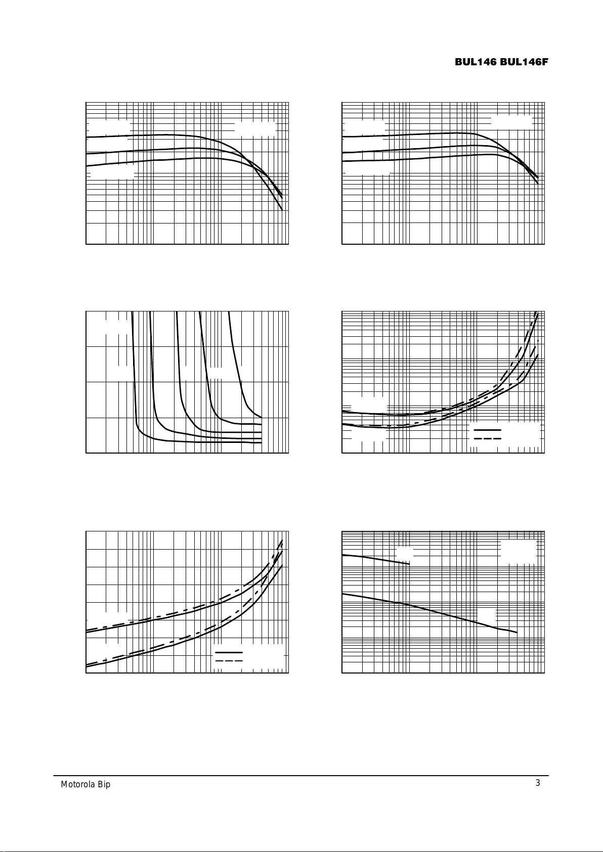
h
FE
, DC CURRENT GAIN
I
C
, COLLECTOR CURRENT (AMPS)
T
J
= 125
°
C
C, CAPACITANCE (pF)
0.01
100
I
C
, COLLECTOR CURRENT (AMPS)
Figure 1. DC Current Gain @ 1 Volt
h
FE
, DC CURRENT GAIN
Figure 2. DC Current Gain @ 5 Volts
V
CE
, VOLTAGE (V)
Figure 3. Collector Saturation Region Figure 4. Collector–Emitter Saturation Voltage
Figure 5. Base–Emitter Saturation Region Figure 6. Capacitance
10
1
1 10
100
10
1
0.01 0.1 1 10
2
0.01
I
B
, BASE CURRENT (mA)
10
1
0.01
0.01
I
C
COLLECTOR CURRENT (AMPS)
0.1
1.2
1
0.8
0.4
0.01
I
C
, COLLECTOR CURRENT (AMPS)
0.1 1 10
1000
100
1
V
CE
, COLLECTOR–EMITTER VOLTAGE (VOLTS)
1 1000
1
0
0.1
1 10
10000
10
0.1
0.1 1 10
10 100
T
J
= 25
°
C
T
J
= – 20
°
C
V
CE
= 1 V
T
J
= 125
°
C
T
J
= 25
°
C
T
J
= – 20
°
C
V
CE
= 5 V
I
C
= 1 A 2 A 3 A
V
CE
, VOLTAGE (V)
I
C
/I
B
= 10
I
C
/I
B
= 5
T
J
= 25
°
C
T
J
= 125
°
C
V
BE
, VOLTAGE (V)
1.1
0.9
0.7
0.6
T
J
= 25
°
C
T
J
= 125
°
C
I
C
/I
B
= 5
I
C
/I
B
= 10
5 A 6 A
T
J
= 25
°
C
0.5
TYPICAL STATIC CHARACTERISTICS
T
J
= 25
°
C
f = 1 MHz
C
ob
C
ib
 Loading...