


Integrated Device Technology Inc IDT54841CP, IDT54841AL, IDT54841ALB, IDT54841AP, IDT54841APB Datasheet
...®
Integrated Device Technology, Inc.
HIGH-PERFORMANCE |
IDT54/74FCT841A/B/C |
CMOS BUS INTERFACE |
|
LATCHES |
|
|
|
FEATURES:
•Equivalent to AMD’s Am29841-46 bipolar registers in pinout/function, speed and output drive over full temperature and voltage supply extremes
•IDT54/74FCT841A equivalent to FAST™ speed
•IDT54/74FCT841B 25% faster than FAST
•IDT54/74FCT841C 40% faster than FAST
•Buffered common latch enable, clear and preset inputs
•IOL = 48mA (commercial) and 32mA (military)
•Clamp diodes on all inputs for ringing suppression
•CMOS power levels (1mW typ. static)
•TTL input and output level compatible
•CMOS output level compatible
•Substantially lower input current levels than AMD’s bipolar Am29800 series (5μA max.)
•Product available in Radiation Tolerant and Radiation Enhanced versions
•Military product compliant to MIL-STD-883, Class B
DESCRIPTION:
The IDT54/74FCT800 series is built using an advanced dual metal CMOS technology.
The IDT54/74FCT840 series bus interface latches are designed to eliminate the extra packages required to buffer existing latches and provide extra data width for wider address/ data paths or buses carrying parity. The IDT54/74FCT841 is a buffered, 10-bit wide version of the popular ‘373 function.
All of the IDT54/74FCT800 high-performance interface family are designed for high-capacitance load drive capability, while providing low-capacitance bus loading at both inputs and outputs. All inputs have clamp diodes and all outputs are designed for low-capacitance bus loading in the high-imped- ance state.
FUNCTIONAL BLOCK DIAGRAM
D0 |
DN |
PRE |
|
D P |
D P |
LE Q |
LE Q |
CLR |
CLR |
CLR |
|
LE |
|
OE
Y0 |
YN |
2607 drw 01
The IDT logo is a registered trademark of Integrated Device Technology, Inc.
FAST is a trademark of National Semiconductor Co.
MILITARY AND COMMERCIAL TEMPERATURE RANGES |
APRIL 1994 |
|
©1994 Integrated Device Technology, Inc. |
7.22 |
DSC-4603/2 |
1
IDT54/74FCT841A/B/C |
|
HIGH-PERFORMANCE CMOS BUS INTERFACE LATCHES |
MILITARY AND COMMERCIAL TEMPERATURE RANGES |
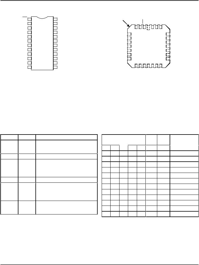
PIN CONFIGURATIONS
OE |
|
1 |
|
24 |
|
VCC |
D0 |
|
2 |
|
23 |
|
Y0 |
|
|
|
||||
D1 |
|
3 |
|
22 |
|
Y1 |
|
|
|
||||
D2 |
|
4 |
P24-1 |
21 |
|
Y2 |
|
|
|||||
D3 |
|
5 |
D24-1 |
20 |
|
Y3 |
|
|
|||||
D4 |
|
6 |
E24-1 |
19 |
|
Y4 |
|
|
|||||
D5 |
|
7 |
& |
18 |
|
Y5 |
|
|
|||||
D6 |
|
8 |
SO24-2 |
17 |
|
Y6 |
|
|
|||||
D7 |
|
9 |
|
16 |
|
Y7 |
|
|
|
||||
D8 |
|
10 |
|
15 |
|
Y8 |
|
|
|
||||
D9 |
|
|
14 |
|
Y9 |
|
|
11 |
|
|
|||
GND |
|
12 |
|
13 |
|
LE |
|
|
|
||||
DIP/CERPACK/SOIC
TOP VIEW
INDEX |
D1 |
D0 OE NC VCC Y0 |
Y1 |
|
||||
|
|
|
|
|
|
|
|
|
D2 |
4 |
3 |
2 |
1 |
28 |
27 |
26 |
Y2 |
5 |
|
|
|
|
|
25 |
||
D3 |
6 |
|
|
|
|
|
24 |
Y3 |
D4 |
7 |
|
L28-1 |
|
23 |
Y4 |
||
NC |
8 |
|
|
22 |
NC |
|||
D5 |
9 |
|
|
|
|
|
21 |
Y5 |
D6 |
10 |
|
|
|
|
|
20 |
Y6 |
D7 |
11 |
|
|
|
|
|
19 |
Y7 |
|
12 |
13 |
14 |
15 |
16 |
17 |
18 |
|
|
D8 |
D9 |
GND NC |
LE |
Y9 |
Y8 |
|
|
|
|
|
LCC |
|
|
|
||
|
|
TOP VIEW |
|
|
||||
2607 drw 02 |
2607 drw 03 |
PIN DESCRIPTION
Name |
I/O |
Description |
CLR |
I |
When CLR is LOW, the outputs are |
|
|
LOW if OE is LOW. When CLR is HIGH, |
|
|
data can be entered into the latch. |
DI |
I |
The latch data inputs. |
LE |
I |
The latch enable input. The latches are |
|
|
transparent when LE is HIGH. Input |
|
|
data is latched on the HIGH-to-LOW |
|
|
transition. |
YI |
O |
The 3-state latch outputs. |
OE |
I |
The output enable control. When OE is |
|
|
LOW, the outputs are enabled. When |
|
|
OE is HIGH, the outputs (Y I) are in the |
|
|
high-impedance (off) state. |
PRE |
I |
Preset line. When PRE is LOW, the |
|
|
outputs are HIGH if OE is LOW. Preset |
|
|
overrides CLR. |
|
|
2607 tbl 01 |
FUNCTION TABLE(1)
|
|
|
|
|
Inter- |
Out- |
|
|
|
Inputs |
|
|
nal |
puts |
|
CLR |
PRE |
OE |
LE |
DI |
QI |
YI |
Function |
H |
H |
H |
X |
X |
X |
Z |
High Z |
H |
H |
H |
H |
L |
L |
Z |
High Z |
H |
H |
H |
H |
H |
H |
Z |
High Z |
H |
H |
H |
L |
X |
NC |
Z |
Latched (High Z) |
H |
H |
L |
H |
L |
L |
L |
Transparent |
H |
H |
L |
H |
H |
H |
H |
Transparent |
H |
H |
L |
L |
X |
NC |
NC |
Latched |
H |
L |
L |
X |
X |
H |
H |
Preset |
L |
H |
L |
X |
X |
L |
L |
Clear |
L |
L |
L |
X |
X |
H |
H |
Preset |
L |
H |
H |
L |
X |
L |
Z |
Latched (High Z) |
H |
L |
H |
L |
X |
H |
Z |
Latched (High Z) |
NOTE: |
|
|
|
|
|
|
2607 tbl 02 |
1.H = HIGH, L = LOW, X = Don’t Care, NC = No Change, Z = High Impedance
7.22 |
2 |

IDT54/74FCT841A/B/C |
|
HIGH-PERFORMANCE CMOS BUS INTERFACE LATCHES |
MILITARY AND COMMERCIAL TEMPERATURE RANGES |
ABSOLUTE MAXIMUM RATINGS(1)
Symbol |
Rating |
Commercial |
Military |
Unit |
VTERM(2) |
Terminal Voltage |
–0.5 to +7.0 |
–0.5 to +7.0 |
V |
|
with Respect to |
|
|
|
|
GND |
|
|
|
VTERM(3) |
Terminal Voltage |
–0.5 to VCC |
–0.5 to VCC |
V |
|
with Respect to |
|
|
|
|
GND |
|
|
|
TA |
Operating |
0 to +70 |
–55 to +125 |
°C |
|
Temperature |
|
|
|
TBIAS |
Temperature |
–55 to +125 |
–65 to +135 |
°C |
|
Under Bias |
|
|
|
TSTG |
Storage |
–55 to +125 |
–65 to +150 |
°C |
|
Temperature |
|
|
|
PT |
Power Dissipation |
0.5 |
0.5 |
W |
IOUT |
DC Output |
120 |
120 |
mA |
|
Current |
|
|
|
NOTE: |
|
|
2607 tbl 03 |
|
1.Stresses greater than those listed under ABSOLUTE MAXIMUM RATINGS may cause permanent damage to the device. This is a stress rating only and functional operation of the device at these or any other conditions above those indicated in the operational sections of this specification is not implied. Exposure to absolute maximum rating conditions for extended periods may affect reliability. No terminal voltage may exceed VCC by +0.5V unless otherwise noted.
2.Input and VCC terminals only.
3.Outputs and I/O terminals only.
CAPACITANCE (TA = +25°C, f = 1.0MHz)
Symbol |
Parameter (1) |
Conditions |
Typ. |
Max. |
Unit |
CIN |
Input |
VIN = 0V |
6 |
10 |
pF |
|
Capacitance |
|
|
|
|
COUT |
Output |
VOUT = 0V |
8 |
12 |
pF |
|
Capacitance |
|
|
|
|
NOTE: |
|
|
|
|
2607 tbl 04 |
1. This parameter is measured at characterization but not tested.
DC ELECTRICAL CHARACTERISTICS OVER OPERATING RANGE
Following Conditions Apply Unless Otherwise Specified: VLC = 0.2V; VHC = VCC – 0.2V
Commercial: TA = 0°C to +70°C, VCC = 5.0V ± 5%; Military: TA = –55°C to +125°C, VCC = 5.0V ± 10%
Symbol |
Parameter |
Test Conditions(1) |
Min. |
Typ.(2) |
Max. |
Unit |
|
VIH |
Input HIGH Level |
Guaranteed Logic HIGH Level |
2.0 |
— |
— |
V |
|
VIL |
Input LOW Level |
Guaranteed Logic LOW Level |
— |
— |
0.8 |
V |
|
II H |
Input HIGH Current |
VCC = Max. |
VI = VCC |
— |
— |
5 |
μA |
|
|
|
VI = 2.7V |
— |
— |
5(4) |
|
II L |
Input LOW Current |
|
VI = 0.5V |
— |
— |
–5(4) |
|
|
|
|
VI = GND |
— |
— |
–5 |
|
IOZH |
Off State (High Impedance) |
VCC = Max. |
VO = VCC |
— |
— |
10 |
μA |
|
Output Current |
|
VO = 2.7V |
— |
— |
10(4) |
|
IOZL |
|
|
VO = 0.5V |
— |
— |
–10(4) |
|
|
|
|
VO = GND |
— |
— |
–10 |
|
VIK |
Clamp Diode Voltage |
VCC = Min., IN = –18mA |
|
— |
–0.7 |
–1.2 |
V |
IOS |
Short Circuit Current |
VCC = Max.(3), VO = GND |
|
–75 |
–120 |
— |
mA |
VOH |
Output HIGH Voltage |
VCC = 3V, VIN = VLC or VHC, IOH = –32μA |
VHC |
VCC |
— |
V |
|
|
|
VCC = Min. |
IOH = –300μA |
VHC |
VCC |
— |
|
|
|
VIN = VIH or VIL |
IOH = –15mA MIL. |
2.4 |
4.3 |
— |
|
|
|
|
IOH = –24mA COM'L. |
2.4 |
4.3 |
— |
|
VOL |
Output LOW Voltage |
VCC = 3V, VIN = VLC or VHC, IOL = 300μA |
— |
GND |
VLC |
V |
|
|
|
VCC = Min. |
IOL = 300μA |
— |
GND |
VLC(4) |
|
|
|
VIN = VIH or VIL |
IOL = 32mA MIL. |
— |
0.3 |
0.5 |
|
|
|
|
IOL = 48mA COM'L. |
— |
0.3 |
0.5 |
|
NOTES: |
|
|
|
|
|
|
2607 tbl 05 |
1.For conditions shown as Max. or Min., use appropriate value specified under Electrical Characteristics for the applicable device type.
2.Typical values are at VCC = 5.0V, +25°C ambient and maximum loading.
3.Not more than one output should be shorted at one time. Duration of the short circuit test should not exceed one second.
4.This parameter is guaranteed but not tested.
7.22 |
3 |
 Loading...