


 Loading...
Burr Brown Products from Texas Instruments
PCM3793
PCM3794
SLES193C – AUGUST 2006 – REVISED FEBRUARY 2007
16-Bit, Low-Power Stereo Audio CODEC With Microphone Bias, Headphone, and Digital
Speaker Amplifier
FEATURES
∙Analog Front End:
–Stereo Single-Ended Input With Multiplexer
–Mono Differential Input
–Stereo Programmable Gain Amplifier
–Microphone Boost Amplifier (20 dB) and Bias
∙Analog BackEnd:
–Stereo/Mono Line Output With Volume
–Stereo/Mono Headphone Amplifier With Volume and Capless Mode
–Stereo/Mono Digital Speaker Amplifier (BTL) With Volume (PCM3793)
∙Analog Performance:
–Dynamic Range: 93 dB (DAC)
–Dynamic Range: 90 dB (ADC)
–40-mW + 40-mW Headphone Output at RL = 16 Ω
–700-mW + 700-mW Speaker Output at RL = 8 Ω
∙Power Supply Voltage
–1.71 V to 3.6 V for Digital I/O Section
–1.71 V to 3.6 V for Digital Core Section
–2.4 V to 3.6 V for Analog Section
–2.4 V to 3.6 V for Power Amplifier Section
∙Low Power Dissipation:
–7 mW in Playback, 1.8 V/2.4 V, 48 kHz
–13 mW in Record, 1.8 V/2.4 V, 48 kHz
–30 μW in Power Down
∙Sampling Frequency: 5 kHz to 50 kHz
∙Automatic Level Control for Recording
∙Operation From a Single Clock Input Without PLL
∙System Clock:
–Common-Audio Clock (256 fS/384 fS), 12/24, 13/26, 13.5/27, 19.2/38.4, 19.68/39.36 MHz
∙Headphone Plug Insert Detection
∙2 (I2C) or 3 (SPI) Wire Serial Control
∙Programmable Function by Register Control:
–Digital Attenuation of DAC: 0 dB to –62 dB
–Power Up/Down Control for Each Module
–6-dB to –70-dB Gain for Analog Outputs
–30-dB to –12-dB Gain for Analog Inputs
–0/20 dB Boost Selectable for Microphone Input
–0-dB to –21-dB Gain for Analog Mixing
–Parameter Settings for ALC
–Three-Band Tone Control and 3D Sound
–High-Pass Filter and Two-Stage Notch Filter
–Analog Mixing
∙Pop-Noise Reduction Circuit
∙Short and Thermal Protection Circuit
∙Package: 5-mm × 5-mm QFN Pacakge
∙Operation Temperature Range: –40°C to 85°C
APPLICATIONS
∙Portable Audio Player, Cellular Phone
∙Video Camcorder, Digital Still Camera
∙PMP/DMB
DESCRIPTION
The PCM3793/94 is a low-power stereo CODEC designed for portable digital audio applications. The device integrates stereo digital speaker amplifier, headphone amplifier, line amplifier, line input, boost amplifier, microphone bias, programmable gain control, analog mixing, sound effects, and automatic level control (ALC). It is available in a small-footprint, 5-mm × 5-mm QFN package. The PCM3793/94 accepts right-justified, left-justified, I2S, and DSP formats, providing easy interfacing to audio DSP, decoder, and encoder chips. Sampling rates up to 50 kHz are supported. The user-programmable functions are accessible through a twoor three-wire serial control port.
Please be aware that an important notice concerning availability, standard warranty, and use in critical applications of Texas Instruments semiconductor products and disclaimers thereto appears at the end of this data sheet.
PRODUCTION DATA information is current as of publication date. |
Copyright © 2006–2007, Texas Instruments Incorporated |
Products conform to specifications per the terms of the Texas |
|
Instruments standard warranty. Production processing does not |
|
necessarily include testing of all parameters. |
|

PCM3793
PCM3794
www.ti.com
SLES193C – AUGUST 2006 – REVISED FEBRUARY 2007
This integrated circuit can be damaged by ESD. Texas Instruments recommends that all integrated circuits be handled with appropriate precautions. Failure to observe proper handling and installation procedures can cause damage.
ESD damage can range from subtle performance degradation to complete device failure. Precision integrated circuits may be more susceptible to damage because very small parametric changes could cause the device not to meet its published specifications.
ORDERING INFORMATION
|
|
PACKAGE |
OPERATION |
PACKAGE |
ORDERING |
|
PRODUCT |
PACKAGE |
TEMPERATURE |
||||
CODE |
MARKING |
NUMBER(1) |
||||
|
|
RANGE |
||||
|
|
|
|
|
||
PCM3793RHB |
32 QFN |
RHB |
–40°C to 85°C |
PCM3793 |
PCM3793RHBT |
|
PCM3793RHBR |
||||||
|
|
|
|
|
||
PCM3794RHB |
32 QFN |
RHB |
–40°C to 85°C |
PCM3794 |
PCM3794RHBT |
|
PCM3794RHBR |
||||||
|
|
|
|
|
(1)For the most current specification and package information, see the TI Web site at www.ti.com.
TRANSPORT MEDIA
Small tape and reel Large tape and reel Small tape and reel
Large tape and reel
ABSOLUTE MAXIMUM RATINGS
over operating free-air temperature range (unless otherwise noted)(1)
|
|
PCM3793/94 |
UNIT |
Supply voltage |
VDD, VIO, VCC, VPA |
–0.3 to 4 |
V |
Ground voltage differences: DGND, AGND, PGND |
±0.1 |
V |
|
Input voltage |
|
–0.3 to 4 |
V |
Input current (any pins except supplies and SPK out) |
±10 |
mA |
|
Ambient temperature under bias |
–40 to 110 |
°C |
|
Storage temperature |
|
–55 to 150 |
°C |
Junction temperature |
|
150 |
°C |
Lead temperature (soldering) |
260 |
°C, 5 s |
|
Package temperature (reflow, peak) |
260 |
°C |
|
(1)Stresses beyond those listed under absolute maximum ratings may cause permanent damage to the device. These are stress ratings only, and functional operation of the device at these or any other conditions beyond those indicated under recommended operating conditions is not implied. Exposure to absolute–maximum–rated conditions for extended periods may affect device reliability.
RECOMMENDED OPERATING CONDITIONS
over operating free-air temperature range (unless otherwise noted)
|
|
|
MIN |
NOM |
MAX |
UNIT |
VCC, VPA |
Analog supply voltage |
|
2.4 |
3.3 |
3.6 |
V |
VDD , VIO |
Digital supply voltage |
|
1.71 |
3.3 |
3.6 |
V |
|
Digital input logic family |
|
|
CMOS |
|
|
|
Digital input clock frequency |
SCKI system clock |
3.072 |
|
18.432 |
MHz |
|
LRCK sampling clock |
8 |
|
48 |
kHz |
|
|
|
|
||||
|
|
LOL and LOR |
10 |
|
|
kΩ |
|
Analog output load resistance |
HPOL and HPOR |
16 |
|
|
Ω |
|
|
SPOLP, SPOLN, SPORP and SPORN |
8 |
|
|
Ω |
|
Analog output load capacitance |
|
|
|
30 |
pF |
|
Digital output load capacitance |
|
|
|
10 |
pF |
TA |
Operating free-air temperature |
|
–40 |
|
85 |
°C |
2 |
Submit Documentation Feedback |

PCM3793
PCM3794
www.ti.com
SLES193C – AUGUST 2006 – REVISED FEBRUARY 2007
ELECTRICAL CHARACTERISTICS
All specifications at TA = 25°C, VDD = VIO = VCC = VPA = 3.3 V, fS = 48 kHz, system clock = 256 fS, and 16-bit data (unless otherwise noted).
|
PARAMETER |
TEST CONDITIONS |
PCM3793RHB, PCM3794RHB |
UNIT |
||
|
MIN |
TYP |
MAX |
|||
|
|
|
|
|||
Audio Data Characteristics |
|
|
|
|
|
|
DATA FORMAT |
|
|
|
|
|
|
|
Resolution |
|
|
16 |
|
Bits |
|
Audio data interface format |
|
I2S, left-, right-justified, DSP |
|
||
|
Audio data bit length |
|
|
16 |
|
Bits |
|
Audio data format |
|
MSB first, 2s complement |
|
||
|
Sampling frequency (fS) |
|
5 |
|
50 |
kHz |
|
System clock |
VDD < 2 V |
|
|
27 |
MHz |
|
VDD > 2 V |
|
|
40 |
||
|
|
|
|
|
||
Digital Input/Output |
|
|
|
|
|
|
|
Logic family |
|
CMOS compatible |
|
|
|
VIH |
Input logic level |
|
0.7 VIO |
|
|
VDC |
VIL |
|
|
|
0.3 VIO |
VDC |
|
|
|
|
|
|||
IIH |
Input logic current |
VIN = 3.3 V |
|
|
10 |
μA |
IIL |
VIN = 0 V |
|
|
–10 |
||
|
|
|
|
|||
VOH |
Output logic level |
IOH = –2 mA |
0.75 VIO |
|
|
VDC |
VOL |
IOL = 2 mA |
|
|
0.25 VIO |
VDC |
|
|
|
|
||||
Digital Input to Line Output Through DAC (LOL, LOR, and MONO)
 RL = 10 kΩ, ALC = OFF, volume = 0 dB, speaker = powered down, analog mixing = disabled
DYNAMIC PERFORMANCE
|
Full-scale output voltage |
0 dB |
|
2.828 |
Vp-p |
|
|
|
1 |
Vrms |
|
|
|
|
|
||
|
Dynamic range |
EIAJ, A-weighted |
|
93 |
dB |
SNR |
Signal-to-noise ratio |
EIAJ, A-weighted |
86 |
93 |
dB |
|
Channel separation |
|
|
91 |
dB |
THD+N |
Total harmonic distortion + noise |
0 dB |
|
0.008% |
|
|
Load resistance |
|
10 |
|
kΩ |
 Line Input to Line Output Through Mixing Path (LOL, LOR, and MONO)
RL = 10 kΩ, ALC = OFF, volume = 0 dB, speaker = powered down, analog mixing = enabled
 DYNAMIC PERFORMANCE
|
Full-scale input and output |
0 dB |
|
2.828 |
Vp-p |
|
voltage |
|
1 |
Vrms |
|
|
|
|
|||
SNR |
Signal-to-noise ratio |
EIAJ, A-weighted |
84 |
93 |
dB |
Submit Documentation Feedback |
3 |
PCM3793
PCM3794
www.ti.com
SLES193C – AUGUST 2006 – REVISED FEBRUARY 2007
ELECTRICAL CHARACTERISTICS (continued)
All specifications at TA = 25°C, VDD = VIO = VCC = VPA = 3.3 V, fS = 48 kHz, system clock = 256 fS, and 16-bit data (unless otherwise noted).
|
PARAMETER |
TEST CONDITIONS |
PCM3793RHB, PCM3794RHB |
||
|
MIN |
TYP |
UNIT |
||
|
|
|
MAX |
||
Digital Input to Headphone Output Through DAC (HPOL and HPOR) |
|
|
|
||
RL = 16 Ω or 32 Ω, ALC = OFF, volume = 0 dB, speaker = powered down, analog mixing = disabled, not capless mode |
|
||||
DYNAMIC PERFORMANCE |
|
|
|
|
|
|
Full-scale output voltage |
0 dB |
|
2.828 |
Vp-p |
|
|
1 |
Vrms |
||
|
|
|
|
||
SNR |
Signal-to-noise ratio |
EIAJ, A-weighted |
84 |
93 |
dB |
THD+N |
Total harmonic distortion + noise |
30 mW, RL = 32 Ω, volume = 0 dB |
|
0.1% |
|
40 mW, RL = 16 Ω, volume = –1 dB |
|
0.03% |
|
||
|
|
|
|
||
|
Load resistance |
|
16 |
|
Ω |
|
|
200 Hz, 140 mVp-p |
|
–40 |
|
PSRR |
Power-supply rejection ratio |
1 kHz, 140 mVp-p |
|
–45 |
dB |
|
|
20 kHz, 140 mVp-p |
|
–32 |
|
 Line Input to Headphone Output Through Mixing Path (HPOL and HPOR)
RL = 16 Ω or 32 Ω, ALC = OFF, volume = 0 dB, speaker = powered down, analog mixing = enabled, not capless mode
 DYNAMIC PERFORMANCE
|
Full-scale output voltage |
0 dB |
|
2.828 |
Vp-p |
|
|
1 |
Vrms |
||
|
|
|
|
||
SNR |
Signal-to-noise ratio |
EIAJ, A-weighted |
84 |
93 |
dB |
|
Load resistance |
|
16 |
|
Ω |
Digital Input to Speaker Output Through DAC (SPOLP, SPOLN, SPORP, and SPORN): PCM3793 |
|
|
|||
RL = 8 Ω, ALC = OFF, volume = 0 dB, headphone = powered down, analog mixing = disabled |
|
|
|
||
DYNAMIC PERFORMANCE |
|
|
|
|
|
|
Full-scale output voltage |
0 dB |
|
2.52 |
Vp-p |
|
|
0.9 |
Vrms |
||
|
|
|
|
||
SNR |
Signal-to-noise ratio |
EIAJ, A-weighted |
84 |
93 |
dB |
THD+N |
Total harmonic distortion + noise |
400 mW, RL = 8Ω, volume = 0 dB |
|
0.3% |
|
|
Load resistance |
|
8 |
|
Ω |
|
|
200 Hz, 140 mVp-p |
|
–50 |
|
PSRR |
Power-supply rejection ratio |
1 kHz, 140 mVp-p |
|
–45 |
dB |
|
|
20 kHz, 140 mVp-p |
|
–25 |
|
Line Input to Speaker Output Through Mixing Path (SPOLP, SPOLN, SPORP, and SPORN): PCM3793 |
|
||||
RL = 8Ω, ALC = OFF, volume = 0 dB, headphone = powered down, analog mixing = enabled |
|
|
|
||
DYNAMIC PERFORMANCE |
|
|
|
|
|
|
Full-scale output voltage |
0 dB |
|
2.52 |
Vp-p |
|
|
0.9 |
Vrms |
||
|
|
|
|
||
SNR |
Signal-to-noise ratio |
EIAJ, A-Weighted |
84 |
93 |
dB |
4 |
Submit Documentation Feedback |

PCM3793
PCM3794
www.ti.com
SLES193C – AUGUST 2006 – REVISED FEBRUARY 2007
ELECTRICAL CHARACTERISTICS (continued)
All specifications at TA = 25°C, VDD = VIO = VCC = VPA = 3.3 V, fS = 48 kHz, system clock = 256 fS, and 16-bit data (unless otherwise noted).
|
PARAMETER |
TEST CONDITIONS |
PCM3793RHB, PCM3794RHB |
UNIT |
||
|
MIN |
TYP |
MAX |
|||
|
|
|
|
|||
Line Input to Digital Output Through ADC (AIN1L/R, AIN2L/R, AIN3L, and AIN3L/R) |
|
|
|
|
||
ALC = OFF, microphone boost = 0 dB, PGA = 0 dB, speaker and headphone = powered down, analog mixing = disabled |
|
|||||
DYNAMIC PERFORMANCE |
|
|
|
|
|
|
|
Full-scale input voltage |
0 dB |
|
2.828 |
|
Vp-p |
|
|
1 |
|
Vrms |
||
|
|
|
|
|
||
|
Dynamic range |
EIAJ, A-weighted |
|
90 |
|
dB |
SNR |
Signal-to-noise ratio |
EIAJ, A-weighted |
83 |
90 |
|
dB |
|
Channel separation |
|
|
87 |
|
dB |
THD+N |
Total harmonic distortion + noise |
–1 dB |
|
0.009% |
|
|
ANALOG INPUT |
|
|
|
|
|
|
|
Center voltage |
|
|
0.5 VCC |
|
V |
|
Input impedance |
|
10 |
20 |
|
kΩ |
Microphone Bias |
|
|
|
|
|
|
ALC = OFF, microphone boost = 0 dB, PGA = 0 dB, speaker and headphone = powered down, analog mixing = disabled |
|
|||||
|
Bias voltage |
|
|
0.75 VCC |
|
V |
|
Bias source current |
|
|
2 |
|
mA |
|
Output noise |
|
|
14 |
|
μV |
Filter Characteristics |
|
|
|
|
|
|
INTERPOLATION FILTER FOR DAC |
|
|
|
|
|
|
|
Pass band |
|
|
|
0.454 fS |
|
|
Stop band |
|
0.546 fS |
|
|
|
|
Pass-band ripple |
|
|
|
±0.04 |
dB |
|
Stop-band attenuation |
|
–50 |
|
|
dB |
|
Group delay |
|
|
19/fs |
|
s |
|
De-emphasis error |
|
|
±0.1 |
|
dB |
ANALOG FILTER FOR DAC |
|
|
|
|
|
|
|
Frequency response |
f = 20 kHz |
|
±0.2 |
|
dB |
DECIMATION FILTER FOR ADC |
|
|
|
|
|
|
|
Pass band |
|
|
|
0.408 fS |
|
|
Stop band |
|
0.591 fS |
|
|
|
|
Pass-band ripple |
|
|
|
±0.02 |
dB |
|
Stop-band attenuation |
f < 3.268 fS |
–60 |
|
|
dB |
|
Group delay |
|
|
17/fS |
|
s |
HIGH-PASS FILTER FOR ADC |
|
|
|
|
|
|
|
|
–3 dB, fc = 4 Hz |
|
3.74 |
|
|
|
|
–0.5 dB, fc = 4 Hz |
|
10.66 |
|
|
|
Frequency response |
–0.1 dB, fc = 4 Hz |
|
24.2 |
|
Hz |
|
–3 dB, fc = 240 Hz |
|
235.68 |
|
||
|
|
|
|
|
||
|
|
–0.5 dB, fc = 240 Hz |
|
609.95 |
|
|
|
|
–0.1 dB, fc = 240 Hz |
|
2601.2 |
|
|
Submit Documentation Feedback |
5 |

PCM3793
PCM3794
www.ti.com
SLES193C – AUGUST 2006 – REVISED FEBRUARY 2007
ELECTRICAL CHARACTERISTICS (continued)
All specifications at TA = 25°C, VDD = VIO = VCC = VPA = 3.3 V, fS = 48 kHz, system clock = 256 fS, and 16-bit data (unless otherwise noted).
|
PARAMETER |
TEST CONDITIONS |
PCM3793RHB, PCM3794RHB |
UNIT |
|||
|
MIN |
TYP |
MAX |
||||
|
|
|
|
||||
Power Supply and Supply Current |
|
|
|
|
|
||
VIO |
|
VIO |
1.71 |
3.3 |
3.6 |
|
|
VDD |
Voltage range |
VDD |
1.71 |
3.3 |
3.6 |
VDC |
|
VCC |
VCC |
2.4 |
3.3 |
3.6 |
|||
|
|
||||||
VPA |
|
VPA |
2.4 |
3.3 |
3.6 |
|
|
|
Supply current |
BPZ input, all active, no load |
|
24.3 |
35 |
mA |
|
|
All inputs are held static |
|
9 |
50 |
μA |
||
|
|
|
|||||
|
Power dissipation |
BPZ input |
|
80.2 |
115.5 |
mW |
|
|
All inputs are held static |
|
30 |
165 |
μW |
||
|
|
|
|||||
Temperature Condition |
|
|
|
|
|
||
|
Operation temperature |
|
–40 |
|
85 |
°C |
|
θJA |
Thermal resistance |
|
|
30 |
|
°C/W |
|
6 |
Submit Documentation Feedback |
www.ti.com
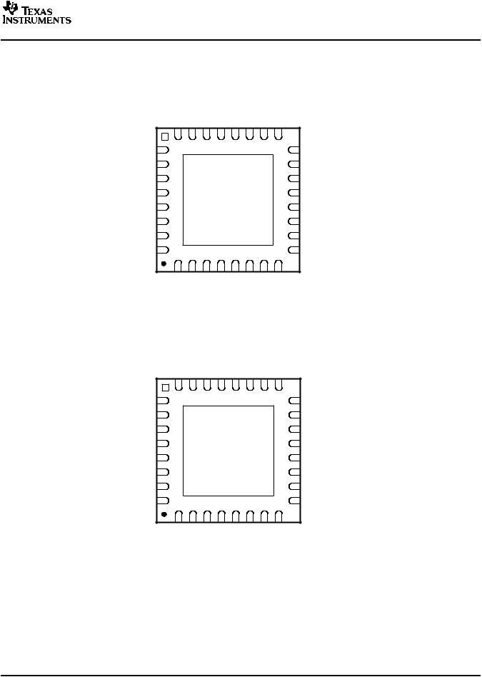
PIN ASSIGNMENTS
AIN2L
AIN1R
AIN1L
MODE
MS/ADR
MD/SDA
MC/SCL
LRCK
AIN2L
AIN1R
AIN1L
MODE
MS/ADR
MD/SDA
MC/SCL
LRCK
PCM3793
PCM3794
SLES193C – AUGUST 2006 – REVISED FEBRUARY 2007
PCM3793RHB (TOP VIEW)
AIN2R |
AIN3L |
AIN3R |
MICB |
V |
AGND |
V |
HPOL/LOL |
|
|
|
|
|
CC |
|
COM |
|
|
24 |
23 |
22 |
21 |
20 |
19 |
18 |
17 |
|
25 |
|
|
|
|
|
|
16 |
HPOR/LOR |
26 |
|
|
|
|
|
|
15 |
SPOLP |
27 |
|
|
|
|
|
|
14 |
SPOLN |
28 |
|
|
|
|
|
|
13 |
PGND |
29 |
|
|
|
|
|
|
12 |
VPA |
30 |
|
|
|
|
|
|
11 |
SPORP |
31 |
|
|
|
|
|
|
10 |
SPORN |
32 |
|
|
|
|
|
|
9 |
HPCOM/MONO |
1 |
2 |
3 |
4 |
5 |
6 |
7 |
8 |
|
BCK |
DIN |
DOUT |
V |
V |
DGND |
SCKI |
HDTI |
|
|
|
|
IO |
DD |
|
|
|
|
|
|
|
|
|
|
|
|
P0048-03 |
|
|
PCM3794RHB |
|
|
|
|||
|
|
(TOP VIEW) |
|
HPOL/LOL |
|
|||
AIN2R |
AIN3L |
AIN3R |
MICB |
V |
AGND |
V |
|
|
|
|
|
|
CC |
|
COM |
|
|
24 |
23 |
22 |
21 |
20 |
19 |
18 |
17 |
|
25 |
|
|
|
|
|
|
16 |
HPOR/LOR |
26 |
|
|
|
|
|
|
15 |
NC |
27 |
|
|
|
|
|
|
14 |
NC |
28 |
|
|
|
|
|
|
13 |
PGND |
29 |
|
|
|
|
|
|
12 |
VPA |
30 |
|
|
|
|
|
|
11 |
NC |
31 |
|
|
|
|
|
|
10 |
NC |
32 |
|
|
|
|
|
|
9 |
HPCOM/MONO |
1 |
2 |
3 |
4 |
5 |
6 |
7 |
8 |
|
BCK |
DIN |
DOUT |
V |
V |
DGND |
SCKI |
HDTI |
|
|
|
|
IO |
DD |
|
|
|
|
|
|
|
|
|
|
|
|
P0048-04 |
Submit Documentation Feedback |
7 |

PCM3793
PCM3794
www.ti.com
SLES193C – AUGUST 2006 – REVISED FEBRUARY 2007
Table 1. TERMINAL FUNCTIONS
|
TERMINAL |
|
I/O |
DESCRIPTION |
|
NAME |
PCM3793RHB |
PCM3794RHB |
|||
|
|
||||
AGND |
19 |
19 |
– |
Ground for analog |
|
AIN1L |
27 |
27 |
I |
Analog input 1 for L-channel |
|
AIN1R |
26 |
26 |
I |
Analog input 1 for R-channel |
|
AIN2L |
25 |
25 |
I |
Analog input 2 for L-channel |
|
AIN2R |
24 |
24 |
I |
Analog input 2 for R-channel |
|
AIN3L |
23 |
23 |
I |
Analog input 3 for L-channel |
|
AIN3R |
22 |
22 |
I |
Analog input 3 for R-channel |
|
BCK |
1 |
1 |
I/O |
Serial bit clock |
|
DGND |
6 |
6 |
– |
Digital ground |
|
DIN |
2 |
2 |
I |
Serial audio data input |
|
DOUT |
3 |
3 |
O |
Serial audio data output |
|
HDTI |
8 |
8 |
I |
Headphone plug insertion detection |
|
HPCOM/MONO |
9 |
9 |
O |
Headphone common/mono line output |
|
HPOL/LOL |
17 |
17 |
O |
Headphone/lineout for R-channel |
|
HPOR/LOR |
16 |
16 |
O |
Headphone/lineout for L-channel |
|
LRCK |
32 |
32 |
I/O |
Left and right channel clock |
|
MC/SCL |
31 |
31 |
I |
Mode control clock for three-wire/two-wire interface |
|
MD/SDA |
30 |
30 |
I/O |
Mode control data for three-wire/two-wire interface |
|
MICB |
21 |
21 |
O |
Microphone bias source output |
|
MODE |
28 |
28 |
I |
Twoor three-wire interface selection (LOW: SPI, HIGH: I2C) |
|
MS/ADR |
29 |
29 |
I |
Mode control select for three-wire/two-wire interface |
|
PGND |
13 |
13 |
– |
Ground for speaker power amplifier |
|
SCKI |
7 |
7 |
I |
System clock |
|
SPOLN |
14 |
– |
O |
Speaker output L-channel for negative (PCM3793) |
|
SPOLP |
15 |
– |
O |
Speaker output L-channel for positive (PCM3793) |
|
SPORN |
10 |
– |
O |
Speaker output R-channel for negative (PCM3793) |
|
SPORP |
11 |
– |
O |
Speaker output R-channel for positive (PCM3793) |
|
VCC |
20 |
20 |
– |
Analog power supply |
|
VCOM |
18 |
18 |
– |
Analog common voltage |
|
VDD |
5 |
5 |
– |
Power supply for digital core |
|
VIO |
4 |
4 |
– |
Power supply for digital I/O |
|
VPA |
12 |
12 |
– |
Power supply for power amplifier |
8 |
Submit Documentation Feedback |

|
|
|
|
|
|
|
|
|
|
|
|
|
|
|
|
|
|
|
|
|
|
|
|
|
|
|
|
|
PCM3793 |
www.ti.com |
|
|
|
|
|
|
|
|
|
|
|
|
|
|
|
|
|
|
|
|
|
|
|
|
|
|
|
|
PCM3794 |
|
|
|
|
|
|
|
|
|
|
|
|
|
|
|
|
|
|
|
|
|
SLES193C – AUGUST 2006 – REVISED FEBRUARY 2007 |
||||||||
|
|
|
|
|
|
|
|
|
|
|
|
|
|
|
|
|
|
|
|
|
|
||||||||
FUNCTIONAL BLOCK DIAGRAM |
|
|
|
|
|
|
|
|
|
|
|
|
|
|
|
|
|
|
|
|
|
|
|
||||||
Possible forPower Up/Down |
PCM3794hasnoSpeakerOutput |
SPL |
SPOLP |
SPOLN |
+6to–70dB |
SPR |
SPORP |
SPORN |
+6to–70dB |
HPL |
|
HPOL/ LOL +6to–70dB |
|
|
|
|
HPR |
HPOR/ LOR |
+6to–70dB |
HPC |
HPCOM |
/MONO |
|
|
|
HDTI |
B0181-01 |
||
|
MC/SCLMD/SDA MS/ADR MODE |
|
|
|
|
|
|
|
|
|
|
|
LOUT |
|
MONO |
|
|
|
ROUT |
|
|
|
MONO |
COM |
|
ToneControlBand-3 HPOL |
NotchFilter HPOR |
|
|
|
C) |
|
|
|
|
|
|
DAL MXL |
|
|
|
|
MXR |
|
|
|
|
|
|
|
|
|
|
||||||
|
2 |
|
|
|
|
|
|
|
|
|
|
|
|
|
|
|
|
|
DecimationFilter |
InterpolationFilter |
DEnhancement-3 |
|
|||||||
|
SerialInterface(SPI/I |
|
|
|
|
|
|
|
ΔΣ |
DAC |
DAR |
ΔΣ |
DAC |
|
|
|
|
V |
|||||||||||
|
|
|
|
|
|
|
|
|
|
SW1 |
|
SW2 |
3 SW |
|
SW6 |
|
SW5 |
SW4 |
|
|
|
|
|
|
|
|
|
|
|
|
|
|
|
|
|
|
|
|
|
|
|
|
|
|
|
|
|
|
|
|
|
|
|
|
|
|
|
|
AGND |
|
|
|
|
|
|
|
|
|
|
|
|
|
|
|
|
|
|
|
|
|
|
|
|
|
|
|
|
|
CC |
|
DIN |
|
|
|
|
|
|
|
|
|
|
|
Digital |
Filter |
|
|
|
Digital |
(1) |
|
|
|
(1) |
|
|
|
|
PGND |
|
|
Interface |
|
|
|
|
|
|
|
|
|
|
|
|
Filter |
|
|
|
|
|
|
|
||||||||
|
DOUTSCKI BCK LRCK |
ATT |
Mute |
PG5 |
ch-LInputAnalog |
|
–21dB0to |
ADL |
PG3 |
DigitalΔΣ |
ADC |
|
ADR |
PG4 |
DigitalΔΣ |
ADC |
PG6 |
RInputAnalog-ch |
|
–21dB0to |
|
|
|
|
|
V |
|||
|
Clock |
Manager |
|
|
|
|
|
|
|
|
V |
||||||||||||||||||
|
|
|
|
|
|
|
|
|
|
|
|
|
|
|
|
|
|
|
|
|
|
|
|
|
|
|
|
|
PA |
|
|
Audio |
|
|
|
|
|
|
|
|
|
|
Filter |
|
|
|
|
(1) |
|
|
|
|
|
|
|
|
|
DGND |
|
|
|
|
|
|
|
|
|
|
|
|
|
|
|
|
|
|
|
Filter |
|
|
|
|
|
|
|
|
|
DD |
|
|
|
|
|
|
|
|
|
|
|
|
|
|
|
|
|
|
|
|
|
|
|
|
|
|
|
|
|
|
V |
|
|
|
|
|
|
|
|
|
|
|
|
|
|
|
|
|
|
|
|
|
|
|
|
|
|
|
|
|
IO |
|
|
PowerUp/Down |
Manager |
|
|
PG1 |
MUX3 |
0or+20dB |
|
|
|
|
+30to–12dB |
|
|
|
+30to–12dB |
|
PG2 |
MUX4 |
0or+20dB |
|
|
|
|
COM |
|
||
|
|
PowerOn |
Reset |
|
|
|
|
|
|
|
|
|
D2S |
|
|
|
|
|
|
|
|
MCB |
Bias |
|
|
V |
|
||
|
|
|
|
|
|
|
MUX1 |
|
|
|
|
|
|
|
|
|
|
|
MUX2 |
|
|
|
|
|
COM |
|
|||
|
|
|
|
|
|
|
|
|
|
|
|
|
|
|
|
|
|
|
|
|
|
|
|
|
|||||
|
|
|
|
|
|
|
|
|
|
|
|
|
|
|
|
|
|
|
|
|
|
|
|
Mic |
|
|
|
|
|
|
|
|
|
|
|
|
AIN3L |
AIN2L AIN1L |
|
|
|
|
|
|
|
|
|
|
AIN1R |
AIN2R |
AIN3R |
|
|
MICB |
|
|
COM |
|
|
|
|
|
|
|
|
|
|
|
|
|
|
|
|
|
|
|
|
|
|
|
V |
|
|||||||
Submit Documentation Feedback |
9 |
PCM3793
PCM3794
www.ti.com
SLES193C – AUGUST 2006 – REVISED FEBRUARY 2007
TYPICAL PERFORMANCE CURVES
All specifications at TA = 25°C, VDD = VIO = VCC = VPA = 3.3 V, fS = 8 to 48 kHz, system clock = 256 fS, and 16-bit data, unless otherwise noted.
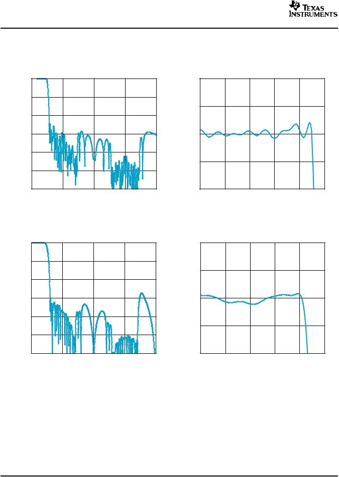
INTERPOLATION FILTER, STOP BAND
|
0 |
|
|
|
|
|
–20 |
|
|
|
|
–dB |
–40 |
|
|
|
|
|
|
|
|
|
|
Amplitude |
–60 |
|
|
|
|
–80 |
|
|
|
|
|
|
|
|
|
|
|
|
–100 |
|
|
|
|
|
–120 |
|
|
|
|
|
0 |
1 |
2 |
3 |
4 |
|
|
|
Frequency [× fS ] |
|
|
|
|
|
|
|
G001 |
Figure 1.
DECIMATION FILTER, STOP BAND
|
0 |
|
|
|
|
|
–20 |
|
|
|
|
–dB |
–40 |
|
|
|
|
|
|
|
|
|
|
Amplitude |
–60 |
|
|
|
|
–80 |
|
|
|
|
|
|
|
|
|
|
|
|
–100 |
|
|
|
|
|
–120 |
|
|
|
|
|
0 |
1 |
2 |
3 |
4 |
|
|
|
Frequency [× fS ] |
|
|
|
|
|
|
|
G003 |
Figure 3.
INTERPOLATION FILTER, PASS BAND
|
0.2 |
|
|
|
|
|
|
0.1 |
|
|
|
|
|
–dB |
|
|
|
|
|
|
Amplitude |
0 |
|
|
|
|
|
|
|
|
|
|
|
|
|
–0.1 |
|
|
|
|
|
|
–0.2 |
|
|
|
|
|
|
0 |
0.1 |
0.2 |
0.3 |
0.4 |
0.5 |
|
|
|
Frequency [× fS ] |
|
|
|
|
|
|
|
|
|
G002 |
Figure 2.
DECIMATION FILTER, PASS BAND
|
0.2 |
|
|
|
|
|
|
0.1 |
|
|
|
|
|
–dB |
|
|
|
|
|
|
Amplitude |
0 |
|
|
|
|
|
|
|
|
|
|
|
|
|
–0.1 |
|
|
|
|
|
|
–0.2 |
|
|
|
|
|
|
0 |
0.1 |
0.2 |
0.3 |
0.4 |
0.5 |
|
|
|
Frequency [× fS ] |
|
|
|
|
|
|
|
|
|
G004 |
Figure 4.
10 |
Submit Documentation Feedback |
PCM3793
PCM3794
www.ti.com
SLES193C – AUGUST 2006 – REVISED FEBRUARY 2007
TYPICAL PERFORMANCE CURVES (continued)
All specifications at TA = 25°C, VDD = VIO = VCC = VPA = 3.3 V, fS = 8 to 48 kHz, system clock = 256 fS, and 16-bit data, unless otherwise noted.
HIGH-PASS FILTER PASS-BAND CHARACTERISTICS
(fC = 4 Hz at fS = 48 kHz)
|
5 |
|
|
|
|
|
0 |
|
|
|
|
dB |
–5 |
|
|
|
|
– |
|
|
|
|
|
|
|
|
|
|
|
Amplitude |
–10 |
|
|
|
|
|
|
|
|
|
|
|
–15 |
|
|
|
|
|
–20 |
|
|
|
|
|
0 |
0.0005 |
0.001 |
0.0015 |
0.002 |
|
|
|
Frequency [× fS ] |
|
|
|
|
|
|
|
G005 |
HIGH-PASS FILTER PASS-BAND CHARACTERISTICS
(fC = 240 Hz at fS = 48 kHz)
|
5 |
|
|
|
|
|
0 |
|
|
|
|
dB |
–5 |
|
|
|
|
– |
|
|
|
|
|
|
|
|
|
|
|
Amplitude |
–10 |
|
|
|
|
|
|
|
|
|
|
|
–15 |
|
|
|
|
|
–20 |
|
|
|
|
|
0 |
0.01 |
0.02 |
0.03 |
0.04 |
|
|
|
Frequency [× fS ] |
|
|
|
|
|
|
|
G006 |
Figure 5. |
Figure 6. |
All specifications at TA = 25°C, VDD = VIO = VCC = VPA = 3.3 V, fS = 44.1 kHz, system clock = 256 fS, and 16-bit data, unless otherwise noted.
Amplitude – dB
THREE-BAND TONE CONTROL (BASS, MIDRANGE,
TREBLE)
15 |
|
|
|
|
|
|
|
10 |
|
|
|
|
|
|
|
5 |
|
|
|
|
|
|
|
0 |
|
|
|
|
|
|
|
–5 |
|
|
|
|
|
|
|
–10 |
|
|
|
|
|
|
|
–15 |
|
|
|
|
|
|
|
0.01 |
0.1 |
1 |
10 |
100 |
1k |
10k |
100k |
|
|
|
Frequency – Hz |
|
|
|
|
|
|
|
|
|
|
|
G007 |
Figure 7.
THREE-BAND TONE CONTROL (BASS)
|
15 |
|
|
|
|
|
|
10 |
|
|
|
|
|
–dB |
5 |
|
|
|
|
|
|
|
|
|
|
|
|
Amplitude |
0 |
|
|
|
|
|
–5 |
|
|
|
|
|
|
|
|
|
|
|
|
|
|
–10 |
|
|
|
|
|
|
–15 |
|
|
|
|
|
|
0 |
200 |
400 |
600 |
800 |
1k |
Frequency – Hz
G008
Figure 8.
Submit Documentation Feedback |
11 |

PCM3793
PCM3794
www.ti.com
SLES193C – AUGUST 2006 – REVISED FEBRUARY 2007
TYPICAL PERFORMANCE CURVES (continued)
All specifications at TA = 25°C, VDD = VIO = VCC = VPA = 3.3 V, fS = 44.1 kHz, system clock = 256 fS, and 16-bit data, unless otherwise noted.
THREE-BAND TONE CONTROL (MIDRANGE)
|
15 |
|
|
|
|
|
|
10 |
|
|
|
|
|
–dB |
5 |
|
|
|
|
|
|
|
|
|
|
|
|
Amplitude |
0 |
|
|
|
|
|
–5 |
|
|
|
|
|
|
|
|
|
|
|
|
|
|
–10 |
|
|
|
|
|
|
–15 |
|
|
|
|
|
|
0 |
1k |
2k |
3k |
4k |
5k |
Frequency – Hz
G009
THREE-BAND TONE CONTROL (TREBLE)
|
15 |
|
|
|
|
|
|
|
10 |
|
|
|
|
|
|
–dB |
5 |
|
|
|
|
|
|
|
|
|
|
|
|
|
|
Amplitude |
0 |
|
|
|
|
|
|
–5 |
|
|
|
|
|
|
|
|
|
|
|
|
|
|
|
|
–10 |
|
|
|
|
|
|
|
–15 |
|
|
|
|
|
|
|
2k |
4k |
6k |
8k |
10k |
12k |
14k |
Frequency – Hz
G010
Figure 9. |
Figure 10. |
All specifications at TA = 25°C, VDD = VIO = VCC = VPA = 3.3 V, fS = 48 kHz, system clock = 256 fS, and 16-bit data, unless otherwise noted.
ADC SNR AT HIGH GAIN (PG1/PG2 = 0 dB)
|
100 |
|
|
90 |
|
|
Single Input |
|
|
85 |
|
dB |
Differential Input |
|
– |
||
70 |
||
SNR |
||
|
||
|
60 |
|
|
50 |
|
|
fIN = 1 kHz |
40
0 |
5 |
10 |
15 |
20 |
25 |
30 |
PG3/PG4 Gain – dB
G011
Figure 11.
ADC SNR AT HIGH GAIN (PG1/PG2 = 20 dB)
|
90 |
|
|
|
|
|
|
|
85 |
|
|
|
|
fIN = 1 kHz |
|
|
80 |
|
|
|
|
|
|
|
75 |
|
|
|
|
|
|
|
|
|
|
Single Input |
|
|
|
–dB |
70 |
|
|
|
|
|
|
65 |
|
|
|
|
|
|
|
SNR |
|
|
|
|
|
|
|
60 |
|
|
|
|
|
|
|
|
|
|
|
|
|
|
|
|
|
|
Differential Input |
|
|
|
|
|
55 |
|
|
|
|
|
|
|
50 |
|
|
|
|
|
|
|
45 |
|
|
|
|
|
|
|
40 |
|
|
|
|
|
|
|
0 |
5 |
10 |
15 |
20 |
25 |
30 |
PG3/PG4 Gain – dB
G012
Figure 12.
12 |
Submit Documentation Feedback |

PCM3793
PCM3794
www.ti.com
SLES193C – AUGUST 2006 – REVISED FEBRUARY 2007
TYPICAL PERFORMANCE CURVES (continued)
All specifications at TA = 25°C, VDD = VIO = VCC = VPA = 3.3 V, fS = 48 kHz, system clock = 256 fS, and 16-bit data, unless otherwise noted.
THD+N – %
|
|
THD+N/SNR vs POWER SUPPLY |
|
|
|
|||||
|
|
DAC TO SPEAKER OUTPUT, 8-Ω |
|
|
|
|||||
1 |
|
|
|
|
|
|
|
|
95 |
|
|
fIN = 1 kHz |
|
|
|
|
|
|
|
||
|
|
|
|
|
|
|
|
|
|
|
0.8 |
|
|
|
|
|
|
|
|
94 |
|
|
|
|
|
|
|
|
|
|
||
0.6 |
|
|
|
|
|
|
|
|
93 |
dB |
|
|
|
THD+N |
|
|
|
|
|||
|
|
|
|
|
|
|
|
|
||
|
|
|
|
|
|
|
|
|
SNR– |
|
0.4 |
|
|
|
|
|
|
|
|
92 |
|
|
|
|
|
|
|
|
|
|
||
|
|
|
|
SNR |
|
|
|
|
|
|
0.2 |
|
|
|
|
|
|
|
|
91 |
|
|
|
|
|
|
|
|
|
|
||
0 |
|
|
|
|
|
|
|
|
90 |
|
|
|
|
|
|
|
|
|
|
||
2 |
2.5 |
3 |
3.5 |
4 |
|
|||||
|
|
|
|
Power Supply – V |
|
|
|
|
|
|
|
|
|
|
|
|
|
|
|
|
G013 |
THD+N – %
|
|
THD+N/SNR vs POWER SUPPLY |
|
|
|
|||||
|
|
DAC TO HEADPHONE OUTPUT, 16-Ω |
|
|
|
|||||
0.05 |
|
|
|
|
|
|
|
|
95 |
|
|
fIN = 1 kHz |
|
|
|
|
|
|
|
||
|
|
|
|
|
|
|
|
|
|
|
0.04 |
|
|
|
|
|
|
|
|
94 |
|
|
|
|
THD+N |
|
|
|
|
|
||
|
|
|
|
|
|
|
|
|
|
|
0.03 |
|
|
|
|
|
|
|
|
93 |
SNR–dB |
|
|
|
|
|
|
|
|
|||
0.02 |
|
|
|
|
|
|
|
|
92 |
|
|
|
|
|
|
|
|
|
|
||
|
|
|
|
SNR |
|
|
|
|
|
|
0.01 |
|
|
|
|
|
|
|
|
91 |
|
|
|
|
|
|
|
|
|
|
||
0 |
|
|
|
|
|
|
|
|
90 |
|
|
|
|
|
|
|
|
|
|
||
2 |
2.5 |
3 |
3.5 |
4 |
|
|||||
|
|
|
|
Power Supply – V |
|
|
|
|
|
|
|
|
|
|
|
|
|
|
|
|
G014 |
|
|
|
|
|
Figure 13. |
|
|
|
|
|
|
|
|
|
THD+N/SNR vs POWER SUPPLY |
|
|
|
|||||
|
|
|
DAC TO LINE OUTPUT, 10-kΩ |
|
|
|
|||||
|
0.012 |
|
|
|
|
|
|
|
|
95 |
|
|
|
fIN = 1 kHz |
|
|
|
|
|
|
|
||
|
|
|
|
|
|
|
|
|
|
|
|
|
0.011 |
|
|
|
|
|
|
|
|
94 |
|
|
|
|
|
|
SNR |
|
|
|
|
||
|
|
|
|
|
|
|
|
|
|
|
|
–% |
0.010 |
|
|
|
|
|
|
|
|
93 |
dB |
|
|
|
|
|
|
|
|
||||
|
|
|
|
|
|
|
|
|
|
||
THD+N |
0.009 |
|
|
|
|
|
|
|
|
92 |
SNR– |
|
|
|
|
THD+N |
|
|
|||||
|
|
|
|
|
|
|
|
|
|
||
|
0.008 |
|
|
|
|
|
|
|
|
91 |
|
|
|
|
|
|
|
|
|
|
|
||
|
0.007 |
|
|
|
|
|
|
|
|
90 |
|
|
|
|
|
|
|
|
|
|
|
||
|
2 |
2.5 |
3 |
3.5 |
4 |
|
|||||
|
|
|
|
|
Power Supply – V |
|
|
|
|
|
|
|
|
|
|
|
|
|
|
|
|
|
G015 |
Figure 15.
|
|
|
|
|
Figure 14. |
|
|
|
|
|
|
|
|
|
THD+N/SNR vs POWER SUPPLY |
|
|
|
|||||
|
|
|
|
ADC TO DIGITAL OUTPUT |
|
|
|
||||
|
0.012 |
|
|
|
|
|
|
|
|
92 |
|
|
|
fIN = 1 kHz |
|
|
|
|
|
|
|
||
|
|
|
|
|
|
|
|
|
|
|
|
|
0.011 |
|
|
|
|
|
|
|
|
91 |
|
|
|
|
|
THD+N |
|
|
|
|
|
||
|
|
|
|
|
|
|
|
|
|
|
|
–% |
0.010 |
|
|
|
|
|
|
|
|
90 |
dB |
|
|
|
|
|
|
|
|
||||
|
|
|
|
|
|
|
|
|
|
||
THD+N |
0.009 |
|
|
|
|
|
|
|
|
89 |
SNR– |
|
|
|
SNR |
|
|
|
|
||||
|
|
|
|
|
|
|
|
|
|
|
|
|
0.008 |
|
|
|
|
|
|
|
|
88 |
|
|
|
|
|
|
|
|
|
|
|
||
|
0.007 |
|
|
|
|
|
|
|
|
87 |
|
|
|
|
|
|
|
|
|
|
|
||
|
2 |
2.5 |
3 |
3.5 |
4 |
|
|||||
|
|
|
|
|
Power Supply – V |
|
|
|
|
|
|
|
|
|
|
|
|
|
|
|
|
|
G016 |
Figure 16.
Submit Documentation Feedback |
13 |

PCM3793
PCM3794
www.ti.com
SLES193C – AUGUST 2006 – REVISED FEBRUARY 2007
TYPICAL PERFORMANCE CURVES (continued)
All specifications at TA = 25°C, VDD = VIO = VCC = VPA = 3.3 V, fS = 48 kHz, system clock = 256 fS, and 16-bit data, unless otherwise noted.
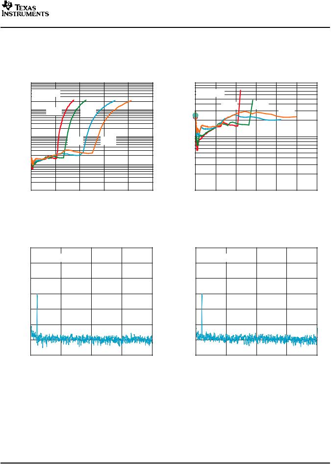
OUTPUT POWER vs POWER SUPPLY (HEADPHONE, 16-Ω)
|
120 |
|
|
|
|
|
|
|
|
|
|
|
fIN = 1 kHz |
|
|
|
|
|
|
|
|
|
|
|
|
|
|
|
|
|
|
|
mW |
100 |
|
|
|
|
|
|
|
|
|
|
|
|
|
|
|
|
|
|
||
80 |
|
|
|
|
|
|
|
|
|
|
– |
|
|
Vol = 6 dB |
|
|
|
|
|
||
|
|
|
|
|
|
|
|
|||
|
|
|
|
|
|
|
|
|
|
|
Power |
60 |
|
|
|
|
|
|
|
|
|
Output |
|
|
|
|
|
|
Vol = 0 dB |
|
|
|
|
|
|
|
|
|
|
|
|
|
|
|
40 |
|
|
|
|
|
|
|
|
|
|
|
|
|
|
|
|
|
|
|
|
|
20 |
|
|
|
|
|
|
|
|
|
|
|
|
|
|
|
|
|
|
|
|
|
0 |
|
|
|
|
|
|
|
|
|
|
|
|
|
|
|
|
|
|
|
|
|
2 |
2.5 |
3 |
3.5 |
4 |
|||||
|
|
|
|
|
Power Supply – V |
|
|
|||
G017
Figure 17.
|
|
THD+N vs OUTPUT POWER |
|
|
|||
|
|
(HEADPHONE, 16-Ω, VOLUME = 6 dB) |
|
||||
|
100 |
|
|
|
|
|
|
|
|
fIN = 1 kHz |
|
|
|
|
|
|
10 |
|
|
3.3 V |
|
|
|
|
|
2.4 V |
|
|
|
|
|
|
|
|
|
|
|
|
|
– % |
|
|
|
2.7 V |
3.6 V |
|
|
THD+N |
1 |
|
|
|
|
||
|
|
|
|
|
|
||
|
|
|
|
|
|
|
|
|
0.1 |
|
|
|
|
|
|
|
0.01 |
|
|
|
|
|
|
|
0 |
20 |
40 |
60 |
80 |
100 |
120 |
Output Power – mW
G019
Figure 19.
OUTPUT POWER vs POWER SUPPLY (SPEAKER, 8-Ω)
|
900 |
|
|
|
|
|
800 |
fIN = 1 kHz |
|
|
|
|
700 |
|
|
|
|
–mW |
|
|
Vol = +6 dB |
|
|
600 |
|
|
|
|
|
|
|
|
|
|
|
Power |
500 |
|
|
|
|
400 |
|
|
|
|
|
Output |
|
|
|
|
|
300 |
|
|
Vol = 0 dB |
|
|
|
|
|
|
|
|
|
200 |
|
|
|
|
|
100 |
|
|
|
|
|
0 |
|
|
|
|
|
2 |
2.5 |
3 |
3.5 |
4 |
Power Supply – V
G018
Figure 18.
|
|
THD+N vs OUTPUT POWER |
|
||
|
|
(HEADPHONE, 16-Ω, VOLUME = 0 dB) |
|
||
|
1 |
|
|
|
|
|
|
fIN = 1 kHz |
|
|
|
– % |
|
2.4 V |
2.7 V |
|
|
|
|
|
|
||
THD+N |
0.1 |
|
|
|
|
|
|
3.3 V |
|
|
|
|
|
|
|
|
|
|
|
|
|
3.6 V |
|
|
0.01 |
|
|
|
|
|
0 |
20 |
40 |
60 |
80 |
Output Power – mW
G020
Figure 20.
14 |
Submit Documentation Feedback |
PCM3793
PCM3794
www.ti.com
SLES193C – AUGUST 2006 – REVISED FEBRUARY 2007
TYPICAL PERFORMANCE CURVES (continued)
All specifications at TA = 25°C, VDD = VIO = VCC = VPA = 3.3 V, fS = 48 kHz, system clock = 256 fS, and 16-bit data, unless otherwise noted.
|
|
THD+N vs OUTPUT POWER |
|
|||
|
|
(SPEAKER, 8-Ω, VOLUME = 6 dB) |
|
|||
|
100 |
|
|
|
|
|
|
|
fIN = 1 kHz |
|
|
|
|
|
10 |
2.4 V |
3.3 V |
|
|
|
|
|
|
|
|
|
|
– % |
|
|
|
|
|
|
THD+N |
1 |
|
2.7 V |
3.6 V |
|
|
|
|
|
|
|||
|
|
|
|
|
|
|
|
0.1 |
|
|
|
|
|
|
0.01 |
|
|
|
|
|
|
0 |
200 |
400 |
600 |
800 |
1000 |
Output Power – mW
G021
Figure 21.
OUTPUT SPECTRUM (DAC TO HEADPHONE OUTPUT, 16-Ω)
|
0 |
|
|
|
|
|
|
fIN = 1 kHz/–60 dB |
|
|
|
|
–20 |
|
|
|
|
|
–40 |
|
|
|
|
–dB |
–60 |
|
|
|
|
Amplitude |
|
|
|
|
|
–80 |
|
|
|
|
|
|
|
|
|
|
|
|
–100 |
|
|
|
|
|
–120 |
|
|
|
|
|
–140 |
|
|
|
|
|
0 |
5 |
10 |
15 |
20 |
Frequency – kHz
G023
Figure 23.
|
|
THD+N vs OUTPUT POWER |
|
|
|||
|
|
(SPEAKER, 8-Ω, VOLUME = 0 dB) |
|
||||
|
1 |
|
|
|
|
|
|
|
|
fIN = 1 kHz |
|
|
|
|
|
|
|
|
2.4 V |
2.7 V |
|
|
|
|
|
|
|
|
3.6 V |
|
|
% |
|
|
|
3.3 V |
|
|
|
– |
|
|
|
|
|
|
|
|
|
|
|
|
|
|
|
THD+N |
0.1 |
|
|
|
|
|
|
|
|
|
|
|
|
|
|
|
0.01 |
|
|
|
|
|
|
|
0 |
100 |
200 |
300 |
400 |
500 |
600 |
Output Power – mW
G022
Figure 22.
OUTPUT SPECTRUM (DAC TO SPEAKER OUTPUT, 8-Ω)
|
0 |
|
|
|
|
|
|
fIN = 1 kHz/–60 dB |
|
|
|
|
–20 |
|
|
|
|
|
–40 |
|
|
|
|
–dB |
–60 |
|
|
|
|
Amplitude |
|
|
|
|
|
–80 |
|
|
|
|
|
|
|
|
|
|
|
|
–100 |
|
|
|
|
|
–120 |
|
|
|
|
|
–140 |
|
|
|
|
|
0 |
5 |
10 |
15 |
20 |
Frequency – kHz
G024
Figure 24.
Submit Documentation Feedback |
15 |

PCM3793
PCM3794
www.ti.com
SLES193C – AUGUST 2006 – REVISED FEBRUARY 2007
PCM3793/94 DESCRIPTION
Analog Input
The AIN1L, AIN1R, AIN2L, AIN2R, AIN3L, and AIN3R pins can be used as microphone or line inputs with selectable 0- or 20-dB boost and 1-Vrms input. All analog inputs have high input impedance (20 kΩ), which is not changed by gain settings. One pair of inputs is selected by register 87 (AIL[1:0], AIR[1:0]). AIN1L and AIN1R can be used as monaural differential inputs.
Gain Settings for Analog Input
Analog signals can be adjusted from 30 dB to –12 dB in 1-dB steps following the 0- or 20-dB boost amplifier. The gain level can be set for each channel by registers 79 and 80 (ALV[5:0], ARV[5:0]).
A/D Converter
The ADC includes a multilevel delta-sigma modulator, aliasing filter, decimation filter, high-pass filter, and notch filter and can accept a 1-Vrms full-scale voltage input. The decimation filter has a digital soft mute controlled by register 81 (RMUL, RMUR). The high-pass filter can be disabled by register 81 (HPF[1:0]) and the notch filter can be disabled by registers 96 to 104 if it is not necessary to cancel a dc offset or compensate for wind noise.
D/A Converter
The DAC includes a multilevel delta-sigma modulator and interpolation filter. These can be used to obtain high PSRR, low jitter sensitivity, and low out-of-band noise quickly and easily. The interpolation filter includes digital attenuator, digital soft mute, three-band tone control (bass, midrange and treble), and 3-D sound controlled by registers 92 to 95. The de-emphasis filter (32, 44.1 and 48 kHz) is controlled by registers 68 to 70 (ATL[5:0], ATR[5:0], PMUL, PMUR, DEM[1:0]). Oversampling rate control can reduce out-of-band noise when operating at low sampling rate by using register 70 (OVER).
Common Voltage
The VCOM pin is normally biased to 0.5 VCC, and it provides the common voltage to internal circuitry. It is recommended that a 10-μF capacitor be connected between this pin and ground to provide clean voltage and
avoid pop noise. The PCM3793/94 may have a little pop noise on each analog output if a capacitor smaller than 10 μF is used.
Line Output
The HPOL/LOL and HPOR/LOR and HPCOM/MONO pins can be used as a monaural single-ended, monaural differential, or stereo single-line output with 1-Vrms output by register 74 (HPS[1:0]). The line outputs can drive a 10-kΩ load. These outputs include an analog volume amplifier, except for the HPCOM/MONO pin that can be set from 6 dB to –70 dB and mute with 0.5-, 1-, 2- or 4-dB steps for each output, as controlled by registers 64 and 65 (HLV[5:0], HRV[5:0], HMUL, HMUR). A dc blocking capacitor is not required when connecting to an external speaker amplifier with monaural differential input. The center voltage is 0.5 VCC with zero data input.
Headphone Output
The HPOL/LOL, HPOR/LOR, and HPCOM/MONO pins are stereo, monaural, or monaural differential headphone outputs with more than 30 or 40 mWrms output power into a 32or 16-Ω load, either through a dc blocking capacitor or without a capacitor, as selected by register 74 (HPS[2:0]). These outputs include analog volume amplifiers, except for the HPCOM/MONO pin, which can be set from 6 dB to –70 dB with 0.5-, 1-, 2- or 4-dB steps for each output using registers 64 and 65 (HLV[5:0], HRV[5:0], HMUL, HMUR). The center voltage is 0.5 VCC with zero data input.
Headphone Plug Insertion Detection
The HDTI pin detects the insertion status of headphone plug and writes the status to register 77 (HPDS), which can be read by the I2C interface. The polarity of the status indication can be inverted by register 75 (HPDP). The headphone and speaker amplifiers are disabled or enabled automatically by headphone plug insertion/extractrion if register 75, HPDE = 1. They are controlled by register settings if register 75, HPDE = 0. HPCOM/MONO is not affected by the status when register 74, CMS[0] = 1.
16 |
Submit Documentation Feedback |

PCM3793
PCM3794
www.ti.com
SLES193C – AUGUST 2006 – REVISED FEBRUARY 2007
Speaker Output (Class-D, PCM3793)
The SPOLP, SPOLN and SPORP, SPORN pins are stereo or mono speaker differential outputs (BTL) with a maximum of 700 mWrms (VPA = 3.6 V, volume = 6 dB) into an 8-Ω load. The digital speaker amplifier offers maximum battery life and minimum heat, eliminates the LC low-pass filter, and includes analog volume amplification for each output from 6 dB to –70 dB with 0.5-, 1-, 2- or 4-dB steps, which can be set by register 66, 67 (SLV[5:0], SLR[5:0]). Spectrum spreading technology and selectable switching frequency to reduce EMI noise is controlled by register 71 (DFQ[2:0], SPS[1:0] and SPSE). The speaker amplifiers have a thermal shutdown circuit which detects when the device temperature reaches approximately 150°C; then the speaker amplifier is powered down.
Analog Mixing and Bypass
Mixing amplifiers (MXL, MXR) mix gain-controlled analog inputs from the AIN pins which have bypassed ADC and DAC and direct the mixed signal to the headphone or speaker outputs. Analog mixing is controlled by register 87 (AD2S, AIR[1:0], AIL[1:0]), register 88 (MXR[2:0], MXL[2:0]), and register 89 (GMR[2:0], GML[2:0]). The analog mixing functions are suitable for FM radio, headset, and another analog sources without an ADC.
Microphone Bias
The MICB pin is the microphone bias source for an external microphone and can provide 2 mA (typical) bias current.
Automatic Level Control (ALC) for Recording
The sound for microphone recording should be expanded to a suitable level without saturation. The digitally controlled automatic level control (ALC) provides automatic expansion for small input signals and compression for large input signals while recording. The expansion level, compression level, attack time, and recovery time can be selected by register 83. The register 83 description explains the details of these settings.
3-D Sound
A 3-D sound effect is provided by mixing L-channel and R-channel data with band pass filter that can be controlled two parameters, mixing ratio and band pass filter characteristic by register 95 (3DP[3:0], 3FLO). The 3-D sound effect can be applied to the DAC digital input or ADC digital output, as selected by register 95 (SDAS).
Three-Band Tone Control
Tone control has bass, midrange, and treble controls that can be adjusted from 12 dB to –12 dB in 1-dB steps by registers 92 to 94 (LGA[4:0], MGA[4:0] and HGA[4:0]). Register 92 (LPAE) attenuates the digital input signal automatically to prevent clipping of the output signal at settings above 0 dB for bass control. LPAE has no effect on midrange and treble controls.
High-Pass Filter and Notch Filter
The high-pass filter eliminates the dc offset of the ADC analog signal and can be set for a cutoff frequency of 4 Hz or 240 Hz at of 48-kHz sampling frequency by register 81 (HPF[1:0]). A register 95 (SDAS) selection applies the filter to either the DAC digital input or the ADC digital output.
Notch filters are provided to remove noise of a particular frequency, such as CCD noise, motor noise, or other mechanical noise in a particualr application. The PCM3793/94 has two notch filters for which the center frequency and frequency bandwidth can be programmed by registers 96 to 104. A register 95 (SDAS) selection applies the filter to either the DAC digital input or the ADC digital output.
Digital Monaural Mixing
Register 96 (MXEN) enables or disables the internal mixing of stereo digital data to monaural digital data.
Zero-Cross Detection
Zero-cross detection minimizes audible zipper noise while changing analog volume and digital attenuation. This function can be applied to digital input or digital output by register 86 (ZCRS).
Submit Documentation Feedback |
17 |

PCM3793
PCM3794
www.ti.com
SLES193C – AUGUST 2006 – REVISED FEBRUARY 2007
Short Protection
The short-circuit protection on each headphone output prevents damage to the device while an output is shorted to VPA, an output is shorted to PGND, or any two outputs are shorted together. When the short circuit is detected on the outputs, the PCM3793/94 powers down the shorted amplifier at once. The short-protection status can be monitored by reading register 77 (STHC, STHL, SCHR) through the I2C interface. Short-circuit protection operates in any enabled headphone amplifier.
Thermal Protection
The thermal protection on the speaker amplifier prevents damage to the device when the internal die temperature exceeds approximately 150°C. Once the die temperature exceeds the thermal set point, all analog outputs are powered down. This status can be reset by setting register 76 (RLSR, RLSL) and can be watched by reading register 77 (STSR, STSL) on the two-wire (I2C) interface. Thermal protection operates in any enabled speaker amplifier.
Pop-Noise Reduction Circuit
The pop-noise reduction circuit prevents audible noise when turning the power supply on/off and powering the device up/down in portable applications. It is recommended to establish the register settings in the sequence that is shown in Table 3 and Table 4. No particular external parts are required, and power-supply sequencing is not necessary.
Power Up/Down for Each Module
Using register 72 (PMXL, PMXR), register 73 (PBIS, PDAR, PDAL, PHPC, PHPR, PHPL, PSPR, PSPL), register 82 (PAIR, PAIL, PADS, PMCB, PADR, PADL), and register 90 (PCOM), unused modules can be powered down to minimize power consumption (7 mW during playback only and 13 mW when recording only).
Digital Interface
All digital I/O pins can interface at various power supply voltages. The VIO pin can be connected to a 1.71-V to 3.6-V power supply.
Power Supply
The VCC pin and the VPA pin can be connected to 2.4 V to 3.6 V. The same voltage must be applied to both pins. The VDD pin and the VIO pin can be connected to 1.71 V to 3.6 V. A different voltage can be applied to each of these pins (for example, VDD = 1.8 V, VIO = 3.3 V).
DESCRIPTION OF OPERATION
System Clock Input
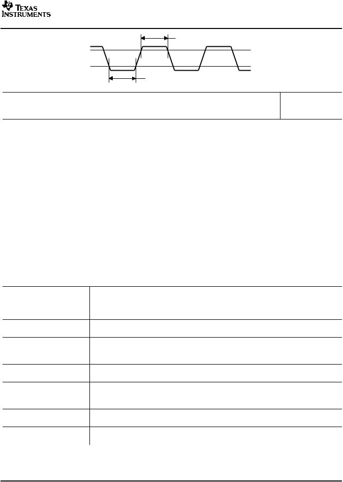
The PCM3793/94 can accept clocks of various frequencies without a PLL. They are used for clocking the digital filters and automatic level control and delta-sigma modulators and are classified as common-audio and application-specific clocks. Table 2 shows frequencies of the common-audio clock and application-specific clock. Figure 25 shows the timing requirements for system clock inputs. The sampling rate and frequency of the system clocks are determined by the settings of register 86 (MSR[2:0]) and register 85 (NPR[5:0]). Note that the sampling rate of the application-specific clock has a little sampling error.
|
Table 2. System Clock Frequencies |
CLOCK |
FREQUENCIES |
Common-audio clock |
11.2896, 12.288, 16.9344, 18.432 MHz |
Application-specific clock |
12, 13, 13.5, 24, 26, 27, 19.2, 19.68, 38.4, 39.36 MHz |
18 |
Submit Documentation Feedback |
PCM3793
PCM3794
www.ti.com
SLES193C – AUGUST 2006 – REVISED FEBRUARY 2007
tw(SCKH)
0.7 VIO
SCKI
0.3 VIO
tw(SCKL)
T0005-12
PARAMETERS |
SYMBOL |
MIN |
UNITS |
System-clock pulse duration, high |
tw(SCKH) |
7 |
ns |
System-clock pulse duration, low |
tw(SCKL) |
7 |
ns |
Figure 25. System Clock Timing
Power-On Reset and System Reset
The power-on-reset circuit outputs a reset signal, typically at VDD = 1.2 V, and this circuit does not depend on the voltage of other power supplies (VCC, VPA and VIO). Internal circuits are cleared to default status, then signals are removed from all analog and digital outputs. The PCM3793/94 does not require any power supply sequencing. Register data must be written after turning all power supplies on.
System reset is enabled by setting register 85 (SRST), and all register are cleared automatically. All circuits are reset to their default status at once. Note that the PCM3793/94 has audible pop noise on the analog outputs when enabling SRST.
Power On/Off Sequence
To reduce audible pop noise, a sequence of register settings is required after turning all power supplies on when powering up, or before turning the power supplies off when powering down. If some modules are not required for a particular application or operation, they should be placed in the power-down state after performing the power-on sequence. The recommended power-on and power-off sequences are shown in Table 3 and Table 4, respectively.
|
|
Table 3. Recommended Power-On Sequence |
STEP |
REGISTER |
NOTE |
|
SETTINGS |
|
1 |
– |
Turn on all power supplies(1) |
2 |
4027h |
Headphone amplifier L-ch volume (–6 dB)(2) |
3 |
4127h |
Headphone amplifier R-ch volume (–6 dB)(2) |
4 |
4227h |
Speaker amplifier L-ch volume (–6 dB)(2) |
5 |
4327h |
Speaker amplifier R-ch volume (–6 dB)(2) |
6 |
4427h |
Digital attenuator L-ch (–24 dB)(2) |
7 |
4527h |
Digital attenuator R-ch (–24 dB)(2) |
8 |
4620h |
DAC audio interface format (left-justified)(3) |
9 |
4BC0h |
Headphone detection enable and inverting polarity. Short and thermal detection enable |
10 |
5102h |
ADC audio interface format (left-justified)(3) |
11 |
5A10h |
VCOM ramp up/down time control. PG1, PG2 gain control (0 dB) |
12 |
49E0h |
DAC (DAL, DAR) and analog bias power up |
13 |
5601h |
Zero-cross detection enable |
14 |
4803h |
Analog mixer (MXL, MXR) power up |
15 |
5811h |
Analog mixer input (SW2, SW5) select |
16 |
49FCh |
Headphone amplifier (HPL, HPR, HPC) power up |
(1)Power supply sequencing is not required. It is recommended to set register data with system clock input after turning all power supplies on.
(2)Any level is acceptable for volume or attenuation. Level should be resumed by register data recorded when system power off.
(3)Audio interface format should be set to match the DSP or decoder being used.
Submit Documentation Feedback |
19 |

PCM3793
PCM3794
www.ti.com
SLES193C – AUGUST 2006 – REVISED FEBRUARY 2007
|
|
Table 3. Recommended Power-On Sequence (continued) |
STEP |
REGISTER |
NOTE |
|
SETTINGS |
|
17 |
4C03h |
Speaker amplifier shut down release |
18 |
4A01h |
VCOM power up |
19 |
523Fh |
Analog front end (ADL, ADR, D2S, MCB, PG1, 2, 5, 6) power up |
20 |
5711h |
Analog input (MUX3, MUX4) select. Analog input (MUX1, MUX2) select |
21 |
4F0Ch |
Analog input L-ch (PG3) volume (0 dB)(2) |
22 |
500Ch |
Analog input R-ch (PG4) volume (0 dB)(2) |
23 |
– |
Any settings for other devices or wait time(4)(5) |
24 |
49FFh |
Speaker amplifier (SPL, SPR) power up (5) |
(4)The PCM3793 requires time for VCOM to reach the common level from GND level. The delay depends on the capacitor value for VCOM and the setting of register 90 CMT[1:0]. Wait time [s] = 4 × CVCOM× RCMT
(5)The PCM3794 does not require this setting because it has no speaker output.
|
|
Table 4. Recommended Power-Off Sequence |
STEP |
REGISTER |
NOTE |
|
SETTINGS |
|
1 |
447Fh |
DAC L-ch digital soft-mute enable(1) |
2 |
457Fh |
DAC R-ch digital soft-mute enable(1) |
3 |
5132h |
ADC L-ch/R-ch digital soft-mute enable, ADC audio interface format (left-justified)(2) |
4 |
5811h |
Analog mixer input (SW2, SW5) Select |
5 |
49FFh |
Headphone amplifier (HPL, HPR, HPC) power up (4), speaker amplifier (SPL, SPR) power up(3)(4) |
6 |
5200h |
Analog front end (ADL, ADR, D2S, MCB, PG1, 2, 5, 6) power down |
7 |
5A10h |
VCOM ramp up/down time control, PG1, PG2 gain control (0 dB) |
8 |
4A00h |
VCOM power down |
9 |
– |
Wait time (100 ms) |
10 |
5A00h |
VCOM ramp up/down time control |
11 |
– |
Wait time (100 ms) |
12 |
5A20h |
VCOM ramp up/down time control |
13 |
– |
Wait time (4000 ms) |
14 |
5A30h |
VCOM ramp up/down time control |
15 |
49E0h |
Headphone amplifier (HPL, HPR, HPC) power down, speaker amplifier (SPL, SPR) power down |
16 |
4800h |
Analog mixer (MXL, MXR) power down |
17 |
4900h |
DAC (DAL, DAR) and analog bias power down |
18 |
– |
Turn off all power supplies(5) |
(1)Any level is acceptable for volume or attenuation.
(2)Audio interface format should be set according to DSP or decoder.
(3)PCM3794 has no speaker amplifier.
(4)These modules must be powered up during the power-down sequence.
(5)Power supply sequencing is not required. It is recommended to turn off all power supply after register settings with system clock input.
Power-Supply Current
The current consumption of the PCM3793/94 depends on power up/down status of each circuit module. In order to reduce the power consumption, disabling each module is recommended when it is not used in an application or operation. Table 5 shows the current consumption in some states.
20 |
Submit Documentation Feedback |
|
|
|
|
|
|
|
PCM3793 |
www.ti.com |
|
|
|
|
|
|
PCM3794 |
|
|
SLES193C – AUGUST 2006 – REVISED FEBRUARY 2007 |
|||||
|
|
|
|||||
Table 5. Power Consumption Table |
|
|
|
|
|||
OPERATION MODE |
|
POWER SUPPLY CURRENT [mA] |
|
PD [mW] |
PD [mW] |
||
|
VDD |
VDD |
VCC |
VPA |
VIO |
TOTAL |
TOTAL |
|
(1.8 V) |
(3.3 V) |
(3.3 V) |
(3.3 V) |
(3.3 V) |
(VDD = 1.8 |
(VDD = 3.3 V) |
|
|
|
|
|
|
V) |
|
All Power Down |
0 |
0 |
0.007 |
0.002 |
0 |
0.03 |
0.03 |
All Active |
2.5 |
5.1 |
7.5 |
11.6 |
0.1 |
67.7 |
80.2 |
PLAYBACK WITH DIGITAL INPUT |
|
|
|
|
|
|
|
Line output and headphone output |
1.18 |
2.51 |
1.79 |
0.54 |
0.09 |
10.1 |
16.3 |
Headphone output with sound effect |
1.81 |
3.84 |
1.79 |
0.54 |
0.09 |
11.2 |
20.7 |
Capless headphone output |
1.18 |
2.51 |
1.8 |
0.75 |
0.09 |
10.8 |
17.0 |
Headphone output with line input (AIN2L/AIN2R) |
1.18 |
2.52 |
2.09 |
0.54 |
0.09 |
11.1 |
17.3 |
Headphone output with mono microphone input (AIN1L, 20 dB) |
1.18 |
2.52 |
2.5 |
0.54 |
0.09 |
12.5 |
18.6 |
Headphone output with mono differential microphone input |
1.18 |
2.52 |
2.8 |
0.54 |
0.09 |
13.4 |
19.6 |
(AIN1L/AIN1R, 20 dB) |
|
|
|
|
|
|
|
Stereo speaker output |
1.21 |
2.58 |
2.18 |
10.94 |
0.09 |
45.8 |
52.1 |
Mono speaker output |
1.20 |
2.57 |
2.01 |
5.61 |
0.09 |
27.6 |
33.9 |
Speaker output with line input (AIN2L/AIN2R) |
1.21 |
2.57 |
2.48 |
10.95 |
0.09 |
46.8 |
53.1 |
Speaker output with mono microphone input (AIN1L, 20 dB) |
1.21 |
2.58 |
2.89 |
10.96 |
0.09 |
48.2 |
54.5 |
Speaker output with mono differential microphone input |
1.2 |
2.58 |
3.2 |
10.98 |
0.09 |
49.3 |
55.6 |
(AIN1L/AIN1R, 20 dB) |
|
|
|
|
|
|
|
PLAYBACK WITHOUT DIGITAL INPUT |
|
|
|
|
|
|
|
Line input (AIN2L/AIN2R) to headphone output |
0 |
0 |
0.76 |
0.53 |
0 |
4.3 |
4.3 |
Mono line input (AIN2L) to headphone output |
0 |
0 |
0.61 |
0.53 |
0 |
3.8 |
3.8 |
Mono microphone Input (AIN1L, 20 dB) to headphone output |
0 |
0 |
1.18 |
0.53 |
0 |
5.6 |
5.6 |
Mono differential microphone input (AIN1L/AIN1R, 20 dB) to |
0 |
0 |
1.48 |
0.53 |
0 |
6.6 |
6.6 |
headphone output |
|
|
|
|
|
|
|
Mono microphone input (AIN1L, 20 dB) to speaker output |
0 |
0 |
1.57 |
10.92 |
0 |
41.2 |
41.2 |
RECORDING |
|
|
|
|
|
|
|
Line input (AIN3L/AIN3R) |
1.86 |
3.89 |
4.58 |
0.13 |
0.1 |
19.2 |
28.7 |
Microphone input (AIN1L/AIN1R, 20 dB) |
1.86 |
3.91 |
5.14 |
0.13 |
0.1 |
21.1 |
30.6 |
Microphone input (AIN1L/AIN1R, 20 dB) with ALC |
2.78 |
5.77 |
5.14 |
0.13 |
0.1 |
22.7 |
36.8 |
Mono microphone input (AIN1L, 20 dB) |
1.4 |
2.93 |
3.6 |
0.13 |
0.1 |
15.2 |
22.3 |
Mono microphone input (AIN1L, 20 dB) with ALC |
2.2 |
4.74 |
3.6 |
0.13 |
0.1 |
16.6 |
28.3 |
Mono differential microphone input (AIN1L/AIN1R, 20 dB) |
1.4 |
2.94 |
3.96 |
0.13 |
0.1 |
16.3 |
23.5 |
Mono differential microphone input (AIN1L/AIN1R, 20 dB) with |
2.2 |
4.74 |
3.96 |
0.13 |
0.1 |
17.8 |
29.5 |
ALC |
|
|
|
|
|
|
|
 Conditions: 48 kHz/256 fS, 16 bits, slave mode, zero data input, no load
Audio Serial Interface
The audio serial interface for the PCM3793/94 comprises LRCK, BCK, DIN, and DOUT. Sampling rate (fS), left and right channel are present on LRCK. DIN receives the serial data for the DAC interpolation filter, and DOUT transmits the serial data from the ADC decimation filter. BCK clocks the transfer of serial audio data on DIN and DOUT in its high-to-low transition. BCK and LRCK should be synchronized with audio system clock. Ideally, it is recommended that they be derived from it.
The PCM3793/94 requires LRCK to be synchronized with the system clock. The PCM3793/94 does not require a specific phase relationship between LRCK and the system clock.
The PCM3793/94 has both master mode and slave mode interface formats, which can be selected by register 84, MSTR. In master mode, the PCM3793/94 generates LRCK and BCK from the system clock.
Audio Data Formats and Timing
The PCM3793/94 supports I2S, right-justified, left-justified and DSP formats. The data formats are shown in Figure 28 and are selected using register 70 (RFM[1:0], PFM[1:0]). All formats require binary 2s-complement, MSB-first audio data. The default format is I2S. Figure 26 shows a detailed timing diagram.
Submit Documentation Feedback |
21 |
Loading...