


QUAD 2-PORT REGISTER
The SN54/74LS398 and SN54/74LS399 are Quad 2-Port Registers. They are the logical equivalent of a quad 2-input multiplexer followed by a quad 4-bit edge-triggered register. A Common Select input selects between two 4-bit input ports (data sources). The selected data is transferred to the output register on the LOW-to-HIGH transition of the Clock input. The SN54/74LS398 features both Q and Q inputs, while the SN54/74LS399 has only Q outputs.
•Select From Two Data Sources
•Fully Positive Edge-Triggered Operation
•Both True and Complemented Outputs on SN54/74LS398
•Input Clamp Diodes Limit High-Speed Termination Effects
CONNECTION DIAGRAM DIP (TOP VIEW)
|
VCC Qd |
Qd |
|
Iod |
|
I1d |
|
I1c |
|
I0c |
|
Qc |
|
Qc |
|
CP |
||||
|
20 |
|
19 |
|
18 |
|
17 |
|
16 |
|
15 |
|
14 |
|
13 |
|
12 |
|
11 |
|
|
|
|
|
|
|
|
|
|
|
|
|
|
|
|
|
|
|
|
|
|
|
|
|
|
|
|
|
|
|
|
|
|
|
|
|
|
|
|
|
|
|
SN54 / 74LS398
|
|
|
|
|
|
|
|
|
|
|
|
|
|
|
|
|
|
|
|
|
|
|
|
|
|
|
|
|
|
|
|
|
|
1 |
|
|
2 |
|
|
3 |
|
4 |
|
|
5 |
|
|
|
6 |
|
7 |
|
8 |
|
|
|
9 |
|
10 |
|
|
||||
|
|
|
|
|
|
|
|
|
|
|
|
|
|
|
|
|
|
|
|
|
|
|
|
|
|
|
|
|
|
|
|
|
|
S |
Qa |
|
Qa |
|
I0a |
|
I1a |
I1b |
I0b |
Qb |
Qb |
|
GND |
|
|||||||||||||||||
|
|
|
|
|
|
|
|
|
|
|
|
|
VCC = PIN 20 |
|
|
|
|
|
|
|
|
|
|
|||||||||
|
|
|
|
|
|
|
|
|
|
|
|
|
GND = |
PIN |
10 |
|
|
|
|
|
|
|
|
|
|
|
||||||
|
VCC |
|
|
Qd |
I0d |
|
I1d |
I1c |
|
I0c |
|
Qc |
|
CP |
|
|||||||||||||||||
|
|
16 |
|
|
15 |
|
14 |
|
|
13 |
|
|
|
12 |
|
|
11 |
|
10 |
|
9 |
|
|
|
||||||||
|
|
|
|
|
|
|
|
|
|
|
|
|
|
|
|
|
|
|
|
|
|
|
|
|
|
|
|
|
|
|
|
|
|
|
|
|
|
|
|
|
|
|
|
|
|
|
|
|
|
|
|
|
|
|
|
|
|
|
|
|
|
|
|
|
|
SN54 / 74LS399
|
|
|
|
|
|
|
|
|
|
|
|
|
|
|
|
|
|
|
|
|
|
|
|
|
|
1 |
|
2 |
|
3 |
|
4 |
|
5 |
|
6 |
|
|
7 |
|
8 |
|
|
|
|
|
|
|
|
|
|
|
|
|
|
|
|
|
|
|
|
|
|
|
|
|
|
|
|
|
|
S |
|
Qa |
|
I0a |
|
I1a |
I1b |
I0b |
|
|
Qb |
GND |
|
|
|||||
|
|
|
|
|
|
|
|
VCC = PIN 16 |
|
|
|
|
|
|
|
|
|
|||||
|
|
|
|
|
|
|
|
GND = |
PIN |
8 |
|
|
|
|
|
|
|
|
|
|||
PIN NAMES |
|
|
|
|
|
|
|
|
|
|
|
|
|
LOADING (Note a) |
|
|||||||
|
|
|
|
|
|
|
|
|
|
|
|
|
|
|
|
|
|
|
|
|||
|
|
|
|
|
|
|
|
|
|
|
|
|
|
|
|
|
HIGH |
LOW |
||||
|
|
|
|
|
|
|
|
|
|
|
|
|
|
|||||||||
S |
Common Select Input |
|
|
|
|
|
|
0.5 |
U.L. |
0.25 |
U.L. |
|||||||||||
CP |
Clock (Active HIGH Going Edge) Input |
0.5 |
U.L. |
0.25 |
U.L. |
|||||||||||||||||
I0a ± I0d |
Data Inputs From Source 0 |
|
|
|
0.5 |
U.L. |
0.25 |
U.L. |
||||||||||||||
I1a ± I0d |
Data Inputs From Source 1 |
|
|
|
0.5 |
U.L. |
0.25 |
U.L. |
||||||||||||||
Qa ± Qd |
Register True Outputs (Note b) |
|
|
|
10 |
U.L. |
5 (2.5) |
U.L. |
||||||||||||||
Qa ± Qd |
Register Complementary Outputs |
|
|
|
|
|
|
|
|
|
|
|||||||||||
|
(Note b) |
|
|
|
|
|
|
|
|
|
|
10 |
U.L. |
5 (2.5) |
U.L. |
|||||||
|
|
|
|
|
|
|
|
|
|
|
|
|
|
|
|
|
|
|
|
|
|
|
NOTES:
a)1 TTL Unit Load (U.L.) = 40 μA HIGH/1.6 mA LOW.
b)The Output LOW drive factor is 2.5 U.L. for Military (54) and 5 U.L. for Commercial (74) Temperature Ranges.
SN54/74LS398
SN54/74LS399
QUAD 2-PORT REGISTER
LOW POWER SCHOTTKY
|
|
|
J SUFFIX |
|
|
|
CERAMIC |
|
|
|
CASE 620-09 |
16 |
1 |
|
|
|
|
|
|
|
|
|
N SUFFIX |
|
|
|
PLASTIC |
16 |
|
|
CASE 648-08 |
|
|
|
|
|
1 |
|
|
|
|
|
D SUFFIX |
|
16 |
|
SOIC |
|
|
CASE 751B-03 |
|
|
|
1 |
|
|
|
|
|
|
|
|
J SUFFIX |
|
|
|
CERAMIC |
20 |
|
|
CASE 732-03 |
|
|
|
|
1 |
|
|
|
|
|
|
N SUFFIX |
|
|
|
PLASTIC |
20 |
|
|
CASE 738-03 |
|
|
|
|
1 |
|
|
|
|
|
|
DW SUFFIX |
20 |
|
|
SOIC |
|
|
CASE 751D-03 |
|
|
|
1 |
|
|
|
|
ORDERING INFORMATION
SN54LSXXXJ Ceramic
SN74LSXXXN Plastic
SN74LSXXXDW SOIC
SN74LSXXXD SOIC
FAST AND LS TTL DATA
5-557
SN54/74LS398 •SN54/74LS399
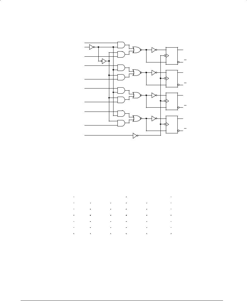
FUNCTIONAL BLOCK DIAGRAM
IOA |
|
S |
|
S |
QA |
IIA |
|
R |
QA |
IOB |
|
S |
QB |
IIB |
|
R |
QB |
IOC |
|
S |
QC |
IIC |
|
R |
QC |
IOD |
|
S |
QD |
IID |
|
R |
QD |
* SN54 / 74LS398 only
FUNCTIONAL DESCRIPTION
The SN54/74LS398 and SN54/74LS399 are high-speed Quad 2-Port Registers. They select four bits of data from two sources (Ports) under the control of a common Select Input
(S). The selected data is transferred to a 4-Bit Output Register synchronous with the LOW-to-HIGH transition of the Clock in-
put (CP). The 4-Bit RS type output register is fully edge-trig- gered. The Data inputs (I) and Select inputs (S) must be stable only a setup time prior to and hold time after the LOW-to-HIGH transition of the Clock input for predictable operation. The SN54/74LS398 has both Q and Q Outputs available.
FUNCTION TABLE
|
INPUTS |
|
|
OUTPUTS |
|
|
|
|
|
|
|
S |
I0 |
I1 |
Q |
|
Q* |
I |
I |
X |
L |
|
H |
|
|
|
|
|
|
I |
h |
X |
H |
|
L |
|
|
|
|
|
|
h |
X |
I |
L |
|
H |
|
|
|
|
|
|
h |
X |
h |
H |
|
L |
|
|
|
|
|
|
*SN54 / 74LS398 only
I = LOW Voltage Level one setup time pior to the LOW-to-HIGH clock transition h = HIGH Voltage Level one setup time prior to the LOW-to-HIGH clock transition L = LOW Voltage Level
H = HIGH Voltage Level X = Immaterial
FAST AND LS TTL DATA
5-558
 Loading...