


MOTOROLA SN74LS138D, SN74LS138DR2, SN74LS138M, SN74LS138MEL, SN74LS138ML1 Datasheet
...SN74LS138
1-of-8 Decoder/
Demultiplexer
The LSTTL / MSI SN74LS138 is a high speed 1-of-8 Decoder / Demultiplexer. This device is ideally suited for high speed bipolar memory chip select address decoding. The multiple input enables allow parallel expansion to a 1-of-24 decoder using just three LS138 devices or to a 1-of-32 decoder using four LS138s and one inverter. The LS138 is fabricated with the Schottky barrier diode process for high speed and is completely compatible with all ON Semiconductor TTL families.
•Demultiplexing Capability
•Multiple Input Enable for Easy Expansion
•Typical Power Dissipation of 32 mW
•Active Low Mutually Exclusive Outputs
•Input Clamp Diodes Limit High Speed Termination Effects
GUARANTEED OPERATING RANGES
Symbol |
Parameter |
Min |
Typ |
Max |
Unit |
|
|
|
|
|
|
VCC |
Supply Voltage |
4.75 |
5.0 |
5.25 |
V |
TA |
Operating Ambient |
0 |
25 |
70 |
°C |
|
Temperature Range |
|
|
|
|
|
|
|
|
|
|
IOH |
Output Current ± High |
|
|
± 0.4 |
mA |
IOL |
Output Current ± Low |
|
|
8.0 |
mA |
http://onsemi.com
LOW
POWER
SCHOTTKY
16
1
PLASTIC
N SUFFIX
CASE 648
16
1
SOIC
D SUFFIX
CASE 751B
ORDERING INFORMATION
Device |
Package |
Shipping |
|
|
|
SN74LS138N |
16 Pin DIP |
2000 Units/Box |
|
|
|
SN74LS138D |
16 Pin |
2500/Tape & Reel |
|
|
|
Semiconductor Components Industries, LLC, 1999 |
1 |
Publication Order Number: |
December, 1999 ± Rev. 6 |
|
SN74LS138/D |
SN74LS138
CONNECTION DIAGRAM DIP (TOP VIEW)
|
|
|
|
|
|
VCC |
|
O |
0 |
|
|
|
|
|
|
O |
1 |
|
|
O |
2 |
|
|
|
|
|
O |
3 |
O |
4 |
|
|
|
O |
5 |
|
O |
6 |
||||||||||||
|
16 |
|
15 |
|
|
|
14 |
|
13 |
|
|
12 |
|
|
11 |
|
10 |
|
9 |
|
|
|
||||||||||||||||||||||||||||
|
|
|
|
|
|
|
|
|
|
|
|
|
|
|
|
|
|
|
|
|
|
|
|
|
|
|
|
|
|
|
|
|
|
|
|
|
|
|
|
|
|
|
|
|
|
|
|
|
NOTE: |
|
|
|
|
|
|
|
|
|
|
|
|
|
|
|
|
|
|
|
|
|
|
|
|
|
|
|
|
|
|
|
|
|
|
|
|
|
|
|
|
|
|
|
|
|
|
|
|
|
|
The Flatpak version has the same |
|
|
|
|
|
|
|
|
|
|
|
|
|
|
|
|
|
|
|
|
|
|
|
|
|
|
|
|
|
|
|
|
|
|
|
|
|
|
|
|
|
|
|
|
|
|
|
|
|
|
pinouts (Connection Diagram) as |
|
|
|
|
|
|
|
|
|
|
|
|
|
|
|
|
|
|
|
|
|
|
|
|
|
|
|
|
|
|
|
|
|
|
|
|
|
|
|
|
|
|
|
|
|
|
|
|
|
|
the Dual In-Line Package. |
|
|
|
|
|
|
|
|
|
|
|
|
|
|
|
|
|
|
|
|
|
|
|
|
|
|
|
|
|
|
|
|
|
|
|
|
|
|
|
|
|
|
|
|
|
|
|
|||||
|
1 |
|
2 |
|
|
|
3 |
|
4 |
|
|
5 |
|
|
6 |
|
7 |
|
8 |
|
|
|
||||||||||||||||||||||||||||
|
|
|
|
|
|
A0 |
|
A1 |
|
|
|
|
|
|
A2 |
|
|
|
|
1 |
|
|
|
|
|
|
|
2 |
E3 |
|
|
|
7 GND |
|||||||||||||||||
|
|
|
|
|
|
|
|
|
|
|
|
|
|
|
E |
|
|
|
|
|
E |
|
O |
|||||||||||||||||||||||||||
|
|
|
|
|
|
|
|
|
|
|
|
|
|
|
|
|
|
|
|
|
|
|
|
|
|
|
|
|
|
|
|
|
|
|
|
|
|
|
LOADING (Note a) |
|||||||||||
|
|
|
|
|
|
|
|
|
|
|
|
|
|
|
|
|
|
|
|
|
|
|
|
|
|
|
|
|
|
|
|
|
|
|
|
|
|
|
|
|
|
|
|
|
|
|||||
PIN NAMES |
|
|
|
|
|
|
|
|
|
|
|
|
|
|
|
|
|
|
|
|
|
|
|
|
|
|
|
|
|
|
|
HIGH |
|
|
|
|
LOW |
|
||||||||||||
A0 ± A2 |
|
|
|
Address Inputs |
|
|
|
|
|
|
|
|
|
|
|
|
|
0.5 U.L. |
|
|
|
|
0.25 U.L. |
|||||||||||||||||||||||||||
E |
1, |
E |
2 |
|
|
|
|
|
|
Enable (Active LOW) Inputs |
|
|
0.5 U.L. |
|
|
|
|
0.25 U.L. |
||||||||||||||||||||||||||||||||
E3 |
|
|
|
Enable (Active HIGH) Input |
|
|
0.5 U.L. |
|
|
|
|
0.25 U.L. |
||||||||||||||||||||||||||||||||||||||
O |
0 ± |
O |
7 |
|
|
|
|
Active LOW Outputs |
|
|
|
10 U.L. |
|
|
|
|
5 U.L. |
|||||||||||||||||||||||||||||||||
|
|
|
|
|
|
|
|
|
||||||||||||||||||||||||||||||||||||||||||
NOTES: |
|
|
|
|
|
|
|
|
|
|
|
|
|
|
|
|
|
|
|
|
|
|
|
|
|
|
|
|
|
|
|
|
|
|
|
|
|
|
|
|
|
|
|
|||||||
a) 1 TTL Unit Load (U.L.) = 40 mA HIGH/1.6 mA LOW.
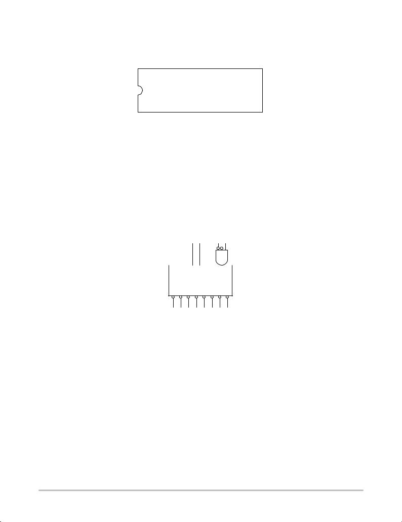
LOGIC SYMBOL
1 |
2 |
3 |
4 5 6 |
||
|
|
|
|
|
|
|
|
|
|
1 2 3 |
|
|
|
|
|||
A |
0 A1 A2 |
E |
|||
O0 O1 O2 O3 O4 O5 O6 O7
15 14 13 12 11 10 9 7
VCC = PIN 16
GND = PIN 8
http://onsemi.com
2

|
|
|
SN74LS138 |
|
|
|
|
|
LOGIC DIAGRAM |
|
|
A2 |
A1 |
A0 |
E1 E2 E3 |
|
|
3 |
2 |
1 |
4 5 |
6 |
VCC = PIN 16 |
|
|
|
|
|
GND = PIN 8 |
|
|
|
|
|
= Pin Numbers |
7 |
9 |
10 |
11 |
12 |
13 |
14 |
15 |
O7 |
|
O6 |
O5 |
O4 O3 |
O2 |
O1 |
O0 |
http://onsemi.com
3
 Loading...