


SN74LS273DWR2
MOTOROLA SN74LS273DWR2, SN74LS273FN, SN74LS273H, SN74LS273M, SN74LS273MEL Datasheet
...
Semiconductor Components Industries, LLC, 1999
December, 1999 – Rev. 6
1 Publication Order Number:
SN74LS273/D
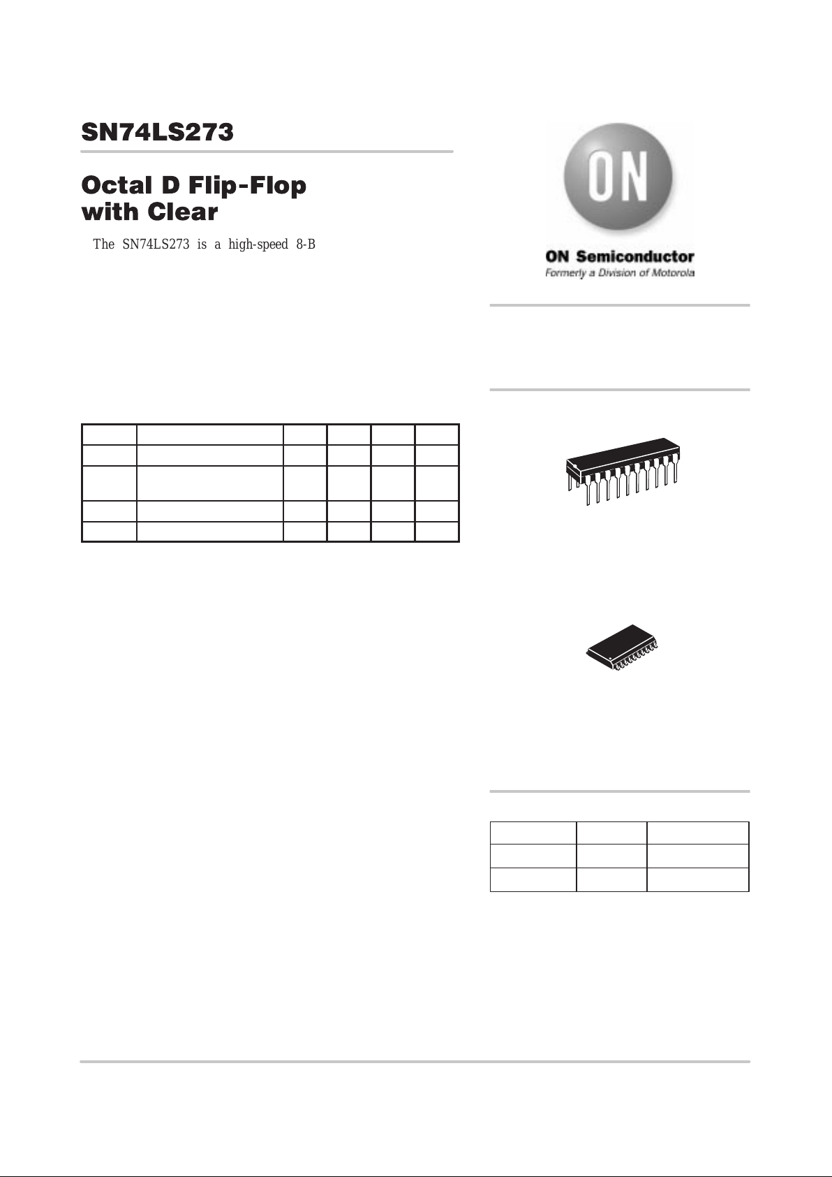
SN74LS273
Octal D Flip-Flop
with Clear
The SN74LS273 is a high-speed 8-Bit Register. The register
consists of eight D-Type Flip-Flops with a Common Clock and an
asynchronous active LOW Master Reset. This device is supplied in a
20-pin package featuring 0.3 inch lead spacing.
• 8-Bit High Speed Register
• Parallel Register
• Common Clock and Master Reset
• Input Clamp Diodes Limit High-Speed Termination Effects
GUARANTEED OPERATING RANGES
Symbol Parameter Min Typ Max Unit
V
CC
Supply Voltage 4.75 5.0 5.25 V
T
A
Operating Ambient
T emperature Range
0 25 70 °C
I
OH
Output Current – High –0.4 mA
I
OL
Output Current – Low 8.0 mA
LOW
POWER
SCHOTTKY
Device Package Shipping
ORDERING INFORMATION
SN74LS273N 16 Pin DIP 1440 Units/Box
SN74LS273DW 16 Pin
SOIC
DW SUFFIX
CASE 751D
http://onsemi.com
2500/Tape & Reel
PLASTIC
N SUFFIX
CASE 738
20
1
20
1
SN74LS273
http://onsemi.com
2
18 17 16 15 14 13
123456
7
20 19
8
V
CC
MR
Q
7
D
7
D
6
Q
6
D
5
Q
5
D
4
Q
0
D
0
D
1
Q
1
Q
2
D
2
D
3
910
Q
3
GND
12 11
Q
4
CP
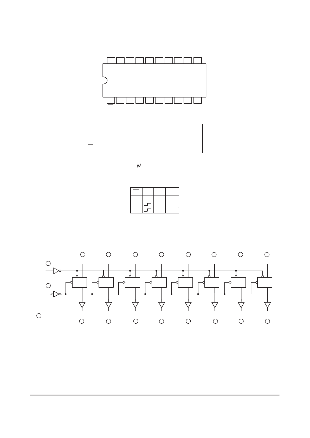
CONNECTION DIAGRAM DIP (TOP VIEW)
Clock (Active HIGH Going Edge) Input
Data Inputs
Master Reset (Active LOW) Input
Register Outputs
CP
D
0
– D
7
MR
Q
0
– Q
7
0.5 U.L.
0.5 U.L.
0.5 U.L.
10 U.L.
0.25 U.L.
0.25 U.L.
0.25 U.L.
5 U.L.
NOTES:
a) 1 TTL Unit Load (U.L.) = 40
m
A HIGH/1.6 mA LOW.
HIGH LOW
(Note a)LOADING
PIN NAMES
TRUTH TABLE
MR CP D
x
Q
x
L X X L
H H H
H L L
H = HIGH Logic Level
L = LOW Logic Level
X = Immaterial
LOGIC DIAGRAM
CP
MR
D
0
D
1
D
2
D
3
D
4
D
5
D
6
D
7
Q
0
Q
1
Q
2
Q
3
Q
4
Q
5
Q
6
Q
7
CP D
CD
Q
CP D
CD
Q
CP D
CD
Q
CP D
CD
Q
CP D
CD
Q
CP D
CD
Q
CP D
CD
Q
CP D
CD
Q
14
1
26
73 84
5 9
11
12
13
15
V
CC
= PIN 20
GND = PIN 10
= PIN NUMBERS
17 18
16 19
SN74LS273
http://onsemi.com
3
FUNCTIONAL DESCRIPTION
The SN74LS273 is an 8-Bit Parallel Register with a
common Clock and common Master Reset.
When the MR input is LOW, the Q outputs are LOW,
independent of the other inputs. Information meeting the
setup and hold time requirements of the D inputs is
transferred to the Q outputs on the LOW-to-HIGH transition
of the clock input.
DC CHARACTERISTICS OVER OPERATING TEMPERATURE RANGE (unless otherwise specified)
Limits
Symbol Parameter
Min Typ Max
Unit Test Conditions
V
IH
Input HIGH Voltage 2.0 V
Guaranteed Input HIGH Voltage for
All Inputs
V
IL
Input LOW Voltage
0.8
V
Guaranteed Input LOW Voltage for
All Inputs
V
IK
Input Clamp Diode Voltage –0.65 –1.5 V V
CC
= MIN, I
IN
= –18 mA
V
OH
Output HIGH Voltage 2.7 3.5 V
V
CC
= MIN, I
OH
= MAX, V
IN
= V
IH
or V
IL
per Truth Table
p
0.25 0.4 V I
OL
= 4.0 mA
V
CC
= V
CC
MIN,
V
OL
O
u
tp
u
t
LOW
Voltage
0.35 0.5 V I
OL
= 8.0 mA
V
IN
=
V
IL
or
V
IH
per Truth Table
p
20 µA V
CC
= MAX, V
IN
= 2.7 V
I
IH
Inp
u
t
HIGH
C
u
rrent
0.1 mA V
CC
= MAX, V
IN
= 7.0 V
I
IL
Input LOW Current –0.4 mA V
CC
= MAX, V
IN
= 0.4 V
I
OS
Short Circuit Current (Note 1) –20 –100 mA V
CC
= MAX
I
CC
Power Supply Current 27 mA V
CC
= MAX
Note 1: Not more than one output should be shorted at a time, nor for more than 1 second.
AC CHARACTERISTICS (T
A
= 25°C, V
CC
= 5.0 V)
Limits
Symbol Parameter
Min Typ Max
Unit Test Conditions
f
MAX
Maximum Input Clock Frequency 30 40 MHz Figure 1
t
PHL
Propagation Delay, MR to Q Output 18 27 ns Figure 2
t
PLH
t
PHL
Propagation Delay, Clock to Output
17
18
27
27
ns Figure 1
AC SETUP REQUIREMENTS (T
A
= 25°C, V
CC
= 5.0 V)
Limits
Symbol Parameter
Min Typ Max
Unit Test Conditions
t
w
Pulse Width, Clock or Clear 20 ns Figure 1
t
s
Data Setup Time 20 ns Figure 1
t
h
Hold Time 5.0 ns Figure 1
t
rec
Recovery Time 25 ns Figure 2
 Loading...