


MOTOROLA SN74LS145D, SN74LS145DR2, SN74LS145M, SN74LS145MEL, SN74LS145ML1 Datasheet
...SN74LS145
1-of-10 Decoder/Driver
Open-Collector
The SN74LS145, 1-of-10 Decoder/Driver, is designed to accept BCD inputs and provide appropriate outputs to drive 10-digit incandescent displays. All outputs remain off for all invalid binary input conditions. It is designed for use as indicator/relay drivers or as an open-collector logic circuit driver. Each of the high breakdown output transistors will sink up to 80 mA of current. Typical power dissipation is 35 mW. This device is fully compatible with all TTL families.
•Low Power Version of 74145
•Input Clamp Diodes Limit High Speed Termination Effects
GUARANTEED OPERATING RANGES
Symbol |
Parameter |
Min |
Typ |
Max |
Unit |
|
|
|
|
|
|
VCC |
Supply Voltage |
4.75 |
5.0 |
5.25 |
V |
TA |
Operating Ambient |
0 |
25 |
70 |
°C |
|
Temperature Range |
|
|
|
|
|
|
|
|
|
|
VOH |
Output Voltage ± High |
|
|
15 |
V |
IOL |
Output Current ± Low |
|
|
24 |
mA |
http://onsemi.com
LOW
POWER
SCHOTTKY
16
1
PLASTIC
N SUFFIX
CASE 648
16
1
SOIC
D SUFFIX
CASE 751B
ORDERING INFORMATION
Device |
Package |
Shipping |
|
|
|
SN74LS145N |
16 Pin DIP |
2000 Units/Box |
|
|
|
SN74LS145D |
16 Pin |
2500/Tape & Reel |
|
|
|
Semiconductor Components Industries, LLC, 1999 |
1 |
Publication Order Number: |
December, 1999 ± Rev. 6 |
|
SN74LS145/D |
SN74LS145
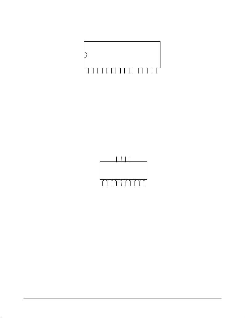
CONNECTION DIAGRAM DIP (TOP VIEW)
|
|
|
|
|
|
|
|
|
|
|
|
|
|
|
|
|
|
|
|
VCC |
|
P0 |
P1 |
|
P2 |
|
P3 |
|
Q9 |
|
Q8 |
|
Q7 |
||||||
16 |
|
15 |
|
14 |
|
13 |
|
12 |
|
11 |
|
10 |
|
9 |
|||||
1 |
2 |
3 |
|
4 |
|
5 |
|
6 |
|
|
7 |
|
8 |
|
|
|||||||
|
|
|
0 |
|
1 |
|
|
2 |
|
3 |
|
|
4 |
|
5 |
|
|
6 |
GND |
|
||
|
|
Q |
Q |
Q |
Q |
Q |
Q |
Q |
|
|||||||||||||
|
|
|
|
|
|
|
|
|
|
|
|
|
|
|
|
|
LOADING (Note a) |
|||||
|
|
|
|
|
|
|
|
|
|
|
|
|
|
|
|
|
|
|
|
|
|
|
PIN NAMES |
|
|
|
|
|
|
|
|
|
|
|
|
|
HIGH |
|
|
LOW |
|||||
P0, P1, P2, P3 |
|
BCD Inputs |
|
|
|
|
|
|
|
|
0.5 U.L. |
|
0.25 U.L. |
|||||||||
Q |
0 ± Q9 |
|
Outputs |
|
|
|
|
|
|
|
Open Collector |
|
15 U.L. |
|||||||||
NOTES:
a) 1 TTL Unit Load (U.L.) = 40 mA HIGH/1.6 mA LOW.
LOGIC SYMBOL
15 14 13 12
P0 P1 P2 P3
Q0 Q1 Q2 Q3 Q4 Q5 Q6 Q7 Q8 Q9
1 |
2 |
3 |
4 |
5 |
6 |
7 |
9 |
10 |
11 |
VCC = PIN 16
GND = PIN 8
http://onsemi.com
2

|
|
|
SN74LS145 |
|
|
|||
|
|
|
LOGIC DIAGRAM |
|
|
|||
|
|
|
INPUTS |
|
|
|
|
|
P0 |
|
|
P1 |
|
P2 |
|
P3 |
|
INPUT |
|
|
|
|
|
|
|
|
INVERTERS |
|
|
|
|
|
|
|
|
0 |
0 |
|
1 |
1 |
2 |
2 |
3 |
3 |
DECODE/DRIVER |
|
|
|
|
|
|
|
|
GATES |
|
|
|
|
|
|
|
|
Q0 |
Q1 |
Q2 |
Q3 |
Q4 |
Q5 |
Q6 |
Q7 |
Q8 Q9 |
|
|
|
|
OUTPUTS |
|
|
|
|
TRUTH TABLE
|
INPUTS |
|
|
|
|
|
|
|
|
|
|
OUTPUTS |
|
|
|
|
|
|
|
|
|||||
|
|
|
|
|
|
|
|
|
|
|
|
|
|
|
|
|
|
|
|
|
|
|
|
|
|
P3 |
P2 |
P1 |
P0 |
|
|
0 |
|
1 |
|
2 |
|
3 |
|
|
4 |
|
5 |
|
6 |
|
7 |
|
8 |
|
9 |
|
Q |
Q |
Q |
Q |
Q |
Q |
Q |
Q |
Q |
Q |
|||||||||||||||
L |
L |
L |
L |
|
L |
H |
H |
H |
|
H |
H |
H |
H |
H |
H |
||||||||||
L |
L |
L |
H |
|
H |
L |
H |
H |
|
H |
H |
H |
H |
H |
H |
||||||||||
L |
L |
H |
L |
|
H |
H |
L |
H |
|
H |
H |
H |
H |
H |
H |
||||||||||
L |
L |
H |
H |
|
H |
H |
H |
L |
|
H |
H |
H |
H |
H |
H |
||||||||||
L |
H |
L |
L |
|
H |
H |
H |
H |
|
L |
H |
H |
H |
H |
H |
||||||||||
L |
H |
L |
H |
|
H |
H |
H |
H |
|
H |
L |
H |
H |
H |
H |
||||||||||
L |
H |
H |
L |
|
H |
H |
H |
H |
|
H |
H |
L |
H |
H |
H |
||||||||||
L |
H |
H |
H |
|
H |
H |
H |
H |
|
H |
H |
H |
L |
H |
H |
||||||||||
H |
L |
L |
L |
|
H |
H |
H |
H |
|
H |
H |
H |
H |
L |
H |
||||||||||
H |
L |
L |
H |
|
H |
H |
H |
H |
|
H |
H |
H |
H |
H |
L |
||||||||||
H |
L |
H |
L |
|
H |
H |
H |
H |
|
H |
H |
H |
H |
H |
H |
||||||||||
H |
L |
H |
H |
|
H |
H |
H |
H |
|
H |
H |
H |
H |
H |
H |
||||||||||
H |
H |
L |
L |
|
H |
H |
H |
H |
|
H |
H |
H |
H |
H |
H |
||||||||||
H |
H |
L |
H |
|
H |
H |
H |
H |
|
H |
H |
H |
H |
H |
H |
||||||||||
H |
H |
H |
L |
|
H |
H |
H |
H |
|
H |
H |
H |
H |
H |
H |
||||||||||
H |
H |
H |
H |
|
H |
H |
H |
H |
|
H |
H |
H |
H |
H |
H |
||||||||||
|
|
|
|
|
|
|
|
|
|
|
|
|
|
|
|
|
|
|
|
|
|
|
|
|
|
H = HIGH Voltage Level
L = LOW Voltage Level
http://onsemi.com
3
 Loading...