Motorola SN54LS256J, SN74LS256D, SN74LS256N Datasheet

DUAL 4-BIT
ADDRESSABLE LATCH
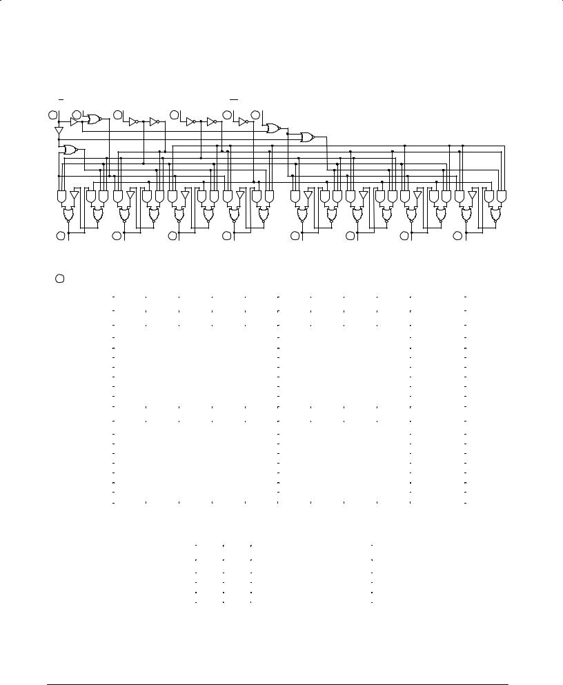
The SN54/74LS256 is a Dual 4-Bit Addressable Latch with common control inputs; these include two Address inputs (A0, A1), an active LOW Enable input
(E) and an active LOW Clear input (CL). Each latch has a Data input (D) and four outputs (Q0 ±Q3).
When the Enable (E) is HIGH and the Clear input (CL) is LOW, all outputs (Q0 ±Q3) are LOW. Dual 4-channel demultiplexing occurs when the (CL) and E are both LOW. When CL is HIGH and E is LOW, the selected output (Q0 ±Q3), determined by the Address inputs, follows D. When the E goes HIGH, the contents of the latch are stored. When operating in the addressable latch mode (E=LOW, CL=HIGH), changing more than one bit of the Address (A0, A1) could impose a transient wrong address. Therefore, this should be done only while in the memory mode (E=CL=HIGH).
•Serial-to-Parallel Capability
•Output From Each Storage Bit Available
•Random (Addressable) Data Entry
•Easily Expandable
•Active Low Common Clear
•Input Clamp Diodes Limit High Speed Termination Effects
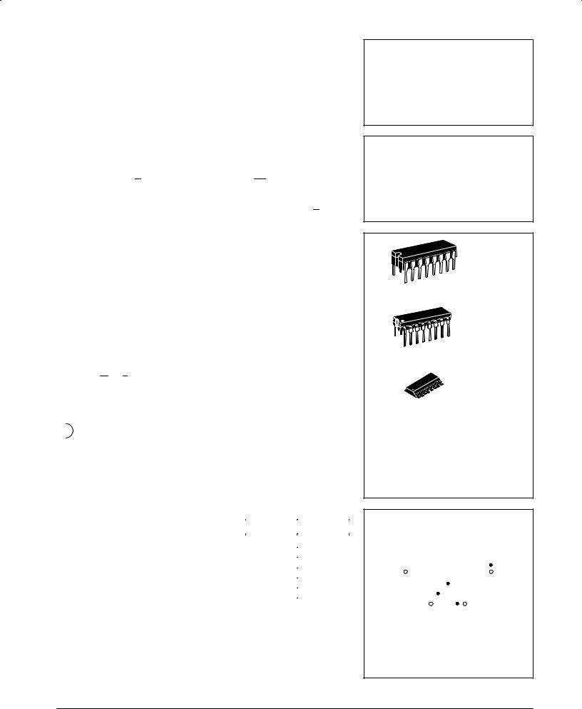
CONNECTION DIAGRAM DIP (TOP VIEW)
|
VCC |
CL |
E |
|
Db |
Q3b |
Q2b |
Q1b |
Q0b |
||||||||
|
16 |
|
15 |
|
14 |
|
13 |
|
12 |
|
11 |
|
10 |
|
9 |
|
|
|
|
|
|
|
|
|
|
|
|
|
|
|
|
|
|
|
NOTE: |
|
|
|
|
|
|
|
|
|
|
|
|
|
|
|
|
|
|
|
|
|
|
|
|
|
|
|
|
|
|
|
|
|
|
|
The Flatpak version |
|
|
|
|
|
|
|
|
|
|
|
|
|
|
|
|
|
has the same pinouts |
|
|
|
|
|
|
|
|
|
|
|
|
|
|
|
|
|
(Connection Diagram) as |
|
|
|
|
|
|
|
|
|
|
|
|
|
|
|
|
|
the Dual In-Line Package. |
|
|
|
|
|
|
|
|
|
|
|
|
|
|
|
|
|
|
|
1 |
|
2 |
|
3 |
|
4 |
|
5 |
|
6 |
|
7 |
|
8 |
|
|
|
|
|
|
|
|
|
|
|
|
|
|
|
|
|
|
|
|
|
A0 |
A1 |
Da |
|
Q0a |
Q1a |
Q2a |
Q3a |
GND |
||||||||
PIN NAMES |
|
LOADING (Note a) |
|
||||
|
|
|
|
HIGH |
LOW |
||
|
|
|
|
|
|
|
|
A0, A1 |
Address Inputs |
0.5 |
U.L. |
0.25 |
U.L. |
||
Da, Db |
Data Inputs |
0.5 |
U.L. |
0.25 |
U.L. |
||
E |
|
|
Enable Input (Active LOW) |
1.0 |
U.L. |
0.5 |
U.L. |
CL |
|
Clear Input (Active LOW) |
0.5 |
U.L. |
0.25 |
U.L. |
|
Q0a |
± Q3a, |
|
|
|
|
|
|
Q0b |
± Q3b |
Parallel Latch Outputs (Note b) |
10 |
U.L. |
5 (2.5) |
U.L. |
|
NOTES:
a)1 TTL Unit Load (U.L.) = 40 μA HIGH/1.6 mA LOW.
b)The Output LOW drive factor is 2.5 U.L. for Military (54) and 5 U.L. for Commercial (74) Temperature Ranges.
SN54/74LS256
DUAL 4-BIT
ADDRESSABLE LATCH
LOW POWER SCHOTTKY
|
|
|
J SUFFIX |
|
|
|
CERAMIC |
|
|
|
CASE 620-09 |
16 |
1 |
|
|
|
|
|
|
|
|
|
N SUFFIX |
|
|
|
PLASTIC |
16 |
|
|
CASE 648-08 |
|
|
|
|
|
1 |
|
|
|
|
|
D SUFFIX |
|
16 |
|
SOIC |
|
|
CASE 751B-03 |
|
|
|
1 |
|
|
|
|
ORDERING INFORMATION
SN54LSXXXJ Ceramic
SN74LSXXXN Plastic
SN74LSXXXD SOIC
LOGIC SYMBOL
|
|
3 |
|
|
2 |
1 |
15 |
|
|
|
14 |
13 |
|
|
|||||||||
|
|
|
|
|
|
|
|
|
|
|
|
|
|
|
|
|
|
|
|
|
|
|
|
|
|
|
|
|
|
|
|
|
|
|
|
|
|
|
|
|
|
|
|
|
|
|
|
|
|
|
|
|
|
|
|
|
|
|
|
|
|
|
|
|
|
|
|
|
|
|
|
|
|
|
|
|
|
|
|
|
|
|
|
|
|
|
|
|
|
|
|
|
|
|
|
|
|
Da |
E |
A0 |
|
|
|
|
|
|
|
|
A0 |
E |
Db |
|
|
||||||
|
|
|
|
|
|
|
|
|
|
|
|
|
|
|
|
|
|
|
|
||||
|
|
|
|
|
|
A1 |
|
|
|
|
|
|
|
A1 |
|
|
|
|
|
|
|||
|
|
|
|
|
|
|
|
|
|
|
|
|
|
|
|
|
|
|
|
||||
|
|
|
|
|
|
CL |
|
|
|
|
|
|
|
|
CL |
|
|
|
|
|
|
||
|
|
|
|
|
|
|
|
|
|
|
|
|
|
|
|
|
|
|
|||||
Q0a Q1a Q2a Q3a |
|
|
|
|
|
|
|
Q0b Q1b Q2b Q3b |
|||||||||||||||
|
|
|
|
|
|
|
|
|
|
|
|
|
|
|
|
|
|
|
|
|
|
|
|
4 |
5 |
6 |
7 |
|
|
|
|
|
|
|
|
9 |
10 |
11 |
12 |
||||||||
|
|
|
|
|
|
|
VCC = PIN 16 |
|
|
|
|
|
|
||||||||||
|
|
|
|
|
|
|
GND |
= |
PIN |
8 |
|
|
|
|
|
|
|
||||||
FAST AND LS TTL DATA
5-421

SN54/74LS256
LOGIC DIAGRAM |
|
|
|
|
|
|
|
|||
E |
|
Da |
A0 |
A1 |
|
CL |
Db |
|
|
|
14 |
3 |
|
1 |
2 |
15 |
|
13 |
|
|
|
4 |
|
|
5 |
6 |
7 |
|
9 |
10 |
11 |
12 |
Q0a |
|
Q1a |
Q2a |
|
Q3a |
Q0b |
Q1b |
Q2b |
Q3b |
|
VCC = PIN 16 |
|
|
|
|
|
|
|
|||
GND |
= |
PIN |
8 |
|
|
|
|
|
|
|
= |
|
PIN |
NUMBERS |
|
|
|
|
|
|
|
TRUTH TABLE
CL |
E |
D |
A0 |
A1 |
Q0 |
Q1 |
Q2 |
Q3 |
MODE |
L |
H |
X |
X |
X |
L |
L |
L |
L |
Clear |
|
|
|
|
|
|
|
|
|
|
L |
L |
L |
L |
L |
L |
L |
L |
L |
Demultiplex |
L |
L |
H |
L |
L |
H |
L |
L |
L |
|
L |
L |
L |
H |
L |
L |
L |
L |
L |
|
L |
L |
H |
H |
L |
L |
H |
L |
L |
|
L |
L |
L |
L |
H |
L |
L |
L |
L |
|
L |
L |
H |
L |
H |
L |
L |
H |
L |
|
L |
L |
L |
H |
H |
L |
L |
L |
L |
|
L |
L |
H |
H |
H |
L |
L |
L |
H |
|
|
|
|
|
|
|
|
|
|
|
H |
H |
X |
X |
X |
QN±1 |
QN±1 |
QN±1 |
QN±1 |
Memory |
H |
L |
L |
L |
L |
L |
QN±1 |
QN±1 |
QN±1 |
Addressable |
H |
L |
H |
L |
L |
H |
QN±1 |
QN±1 |
QN±1 |
Latch |
H |
L |
L |
H |
L |
QN±1 |
L |
QN±1 |
QN±1 |
|
H |
L |
H |
H |
L |
QN±1 |
H |
QN±1 |
QN±1 |
|
H |
L |
L |
L |
H |
QN±1 |
QN±1 |
L |
QN±1 |
|
H |
L |
H |
L |
H |
QN±1 |
QN±1 |
H |
QN±1 |
|
H |
L |
L |
H |
H |
QN±1 |
QN±1 |
QN±1 |
L |
|
H |
L |
H |
H |
H |
QN±1 |
QN±1 |
QN±1 |
H |
|
H = HIGH Voltage Level
L = LOW Voltage Level
X = Immaterial
MODE SELECTION
E |
CL |
MODE |
|
|
|
L |
H |
Addressable Latch |
H |
H |
Memory |
L |
L |
Dual 4-Channel Demultiplexer |
H |
L |
Clear |
|
|
|
FAST AND LS TTL DATA
5-422
 Loading...