


MOTOROLA SN74LS166D, SN74LS166M, SN74LS166MEL, SN74LS166ML1, SN74LS166MR1 Datasheet
...SN74LS166
8-Bit Shift Registers
The SN74LS166 is an 8-Bit Shift Register. Designed with all inputs buffered, the drive requirements are lowered to one 74LS standard load. By utilizing input clamping diodes, switching transients are minimized and system design simplified.
The LS166 is a parallel-in or serial-in, serial-out shift register and has a complexity of 77 equivalent gates with gated clock inputs and an overriding clear input. The shift/load input establishes the parallel-in or serial-in mode. When high, this input enables the serial data input and couples the eight flip-flops for serial shifting with each clock pulse. Synchronous loading occurs on the next clock pulse when this is low and the parallel data inputs are enabled. Serial data flow is inhibited during parallel loading. Clocking is done on the low-to-high level edge of the clock pulse via a two input positive NOR gate, which permits one input to be used as a clock enable or clock inhibit function. Clocking is inhibited when either of the clock inputs are held high, holding either input low enables the other clock input. This will allow the system clock to be free running and the register stopped on command with the other clock input. A change from low-to-high on the clock inhibit input should only be done when the clock input is high. A buffered direct clear input overrides all other inputs, including the clock, and sets all flip-flops to zero.
•Synchronous Load
•Direct Overriding Clear
•Parallel to Serial Conversion
GUARANTEED OPERATING RANGES
Symbol |
Parameter |
Min |
Typ |
Max |
Unit |
|
|
|
|
|
|
VCC |
Supply Voltage |
4.75 |
5.0 |
5.25 |
V |
TA |
Operating Ambient |
0 |
25 |
70 |
°C |
|
Temperature Range |
|
|
|
|
|
|
|
|
|
|
IOH |
Output Current ± High |
|
|
± 0.4 |
mA |
IOL |
Output Current ± Low |
|
|
8.0 |
mA |
http://onsemi.com
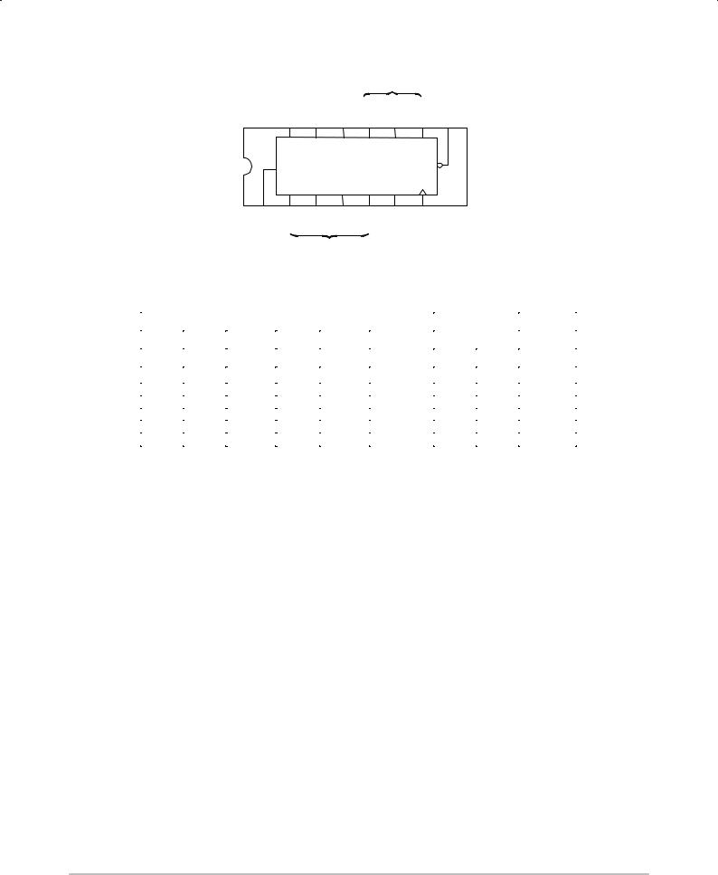
LOW
POWER
SCHOTTKY
16
1
PLASTIC
N SUFFIX
CASE 648
16
1
SOIC
D SUFFIX
CASE 751B
ORDERING INFORMATION
Device |
Package |
Shipping |
|
|
|
SN74LS166N |
16 Pin DIP |
2000 Units/Box |
|
|
|
SN74LS166D |
16 Pin |
2500/Tape & Reel |
|
|
|
Semiconductor Components Industries, LLC, 1999 |
1 |
Publication Order Number: |
December, 1999 ± Rev. 6 |
|
SN74LS166/D |
SN74LS166
|
|
|
|
|
PARALLEL |
|
|
PARALLEL INPUTS |
|
|
|
|||||||||||
|
|
SHIFT/ INPUT OUTPUT |
|
|
|
|
|
|
|
|
|
|
|
|||||||||
|
|
|
|
|
|
|
|
|
|
|
|
|
||||||||||
|
VCC |
LOAD |
H |
QH |
|
G |
|
F |
E |
CLEAR |
||||||||||||
|
16 |
|
|
15 |
|
14 |
|
|
13 |
|
12 |
|
11 |
|
10 |
|
|
9 |
|
|||
|
|
|
SHIFT/ |
H |
QH |
|
G |
|
F |
E |
|
|
|
|||||||||
|
|
|
|
LOAD |
|
|
|
|
|
|
|
|
|
|
|
|
|
|
|
|
|
|
|
|
|
|
SERIAL INPUT |
|
|
|
|
|
|
|
|
CLEAR |
|
|
|
||||||
|
|
|
|
|
|
|
|
|
CLOCK |
|
|
|
|
|
||||||||
|
|
|
|
A |
B |
C |
|
D |
CK |
|
|
|
||||||||||
|
|
|
|
|
INHIBIT |
|
|
|
||||||||||||||
|
|
|
|
|
|
|
|
|
|
|
|
|
|
|
|
|
|
|
|
|
|
|
|
1 |
|
|
2 |
|
3 |
|
|
4 |
|
5 |
|
6 |
|
|
7 |
|
|
8 |
|
||
SERIAL |
|
A |
B |
C |
|
D |
CLOCK CLOCK GND |
|||||||||||||||
INPUT |
|
|
|
|
|
|
|
|
|
|
|
INHIBIT |
|
|
|
|
|
|||||
|
PARALLEL INPUTS |
|
|
|
|
|
||||||||||||||||
|
|
|
|
|
|
|
|
|
|
|
|
|
||||||||||
FUNCTION TABLE
|
|
|
INPUTS |
|
|
INTERNAL |
OUTPUT |
||
|
SHIFT/ |
CLOCK |
|
|
|
PARALLEL |
OUTPUTS |
||
CLEAR |
|
CLOCK |
SERIAL |
|
|
QH |
|||
LOAD |
INHIBIT |
|
A . . . H |
QA |
QB |
||||
|
|
|
|
|
|||||
|
|
|
|
|
|
|
|||
L |
X |
X |
|
X |
X |
X |
L |
L |
L |
H |
X |
L |
|
L |
X |
X |
QA0 |
QB0 |
QH0 |
H |
L |
L |
|
↑ |
X |
a . . . h |
a |
b |
h |
H |
H |
L |
|
↑ |
H |
X |
H |
QAn |
QGn |
H |
H |
L |
|
↑ |
L |
X |
L |
QAn |
QGn |
H |
X |
H |
|
↑ |
X |
X |
QA0 |
QB0 |
QH0 |
http://onsemi.com
2

SN74LS166
Typical Clear, Shift, Load, Inhibit, and Shift Sequences
CLOCK
CLOCK INIHIBIT
CLEAR
SERIAL INPUT
SHIFT/LOAD
A
B
C
PARALLEL D
INPUTS
E
F
G
H OUTPUT QH

 SERIAL SHIFT CLEAR
CLEAR (9) 
SERIAL INPUT
(1)
SHIFT/LOAD
(15)
A (2)
(3)
B
(4)
C
(5)
D
(10)
E
(11)
F
(12)
G
(14)
H
(7)
CLOCK
(6)
CLOCK INHIBIT
H
L
H
L
H
L
H
H
INHIBIT H H |
L |
H |
L |
H |
L |
H |
|
|
|

 SERIAL SHIFT LOAD
R S
CK
QA
R S
CK
QB
R S
CK
QC
R S
CK
QD
R S
CK
QE
R S
CK
QF
R S
CK
QG
R S
CK
(13) QH
http://onsemi.com
3
 Loading...