


Motorola SN54LS191J, SN54LS190J, SN74LS190D, SN74LS190N, SN74LS191D Datasheet
...PRESETTABLE BCD/DECADE UP/DOWN COUNTERS PRESETTABLE 4-BIT BINARY UP/DOWN COUNTERS
The SN54/74LS190 is a synchronous UP/DOWN BCD Decade (8421) Counter and the SN54/74LS191 is a synchronous UP/DOWN Modulo-16 Binary Counter. State changes of the counters are synchronous with the LOW-to-HIGH transition of the Clock Pulse input.
An asynchronous Parallel Load (PL) input overrides counting and loads the data present on the Pn inputs into the flip-flops, which makes it possible to use the circuits as programmable counters. A Count Enable (CE) input serves as the carry /borrow input in multi-stage counters. An Up/Down Count Control (U/D) input determines whether a circuit counts up or down. A Terminal Count (TC) output and a Ripple Clock (RC) output provide overflow/underflow indication and make possible a variety of methods for generating carry/borrow signals in multistage counter applications.
•Low Power . . . 90 mW Typical Dissipation
•High Speed . . . 25 MHz Typical Count Frequency
•Synchronous Counting
•Asynchronous Parallel Load
•Individual Preset Inputs
•Count Enable and Up/Down Control Inputs
•Cascadable
•Input Clamp Diodes Limit High Speed Termination Effects
CONNECTION DIAGRAM DIP (TOP VIEW)
VCC |
|
P0 |
CP |
|
RC |
|
TC |
PL |
P2 |
|
P3 |
|
|
|
|
|
||||||
|
16 |
|
15 |
|
14 |
|
13 |
|
12 |
|
11 |
|
10 |
|
9 |
|
|
|
|
|
|
|
|
|
|
|
|
|
|
|
|
|
|
|
|
|
|
|
|
|
|
NOTE: |
|
|
|
|
|
|
|
|
|
|
|
|
|
|
|
|
|
|
|
|
|
|
|
|
||
|
|
|
|
|
|
|
|
|
|
|
|
|
|
|
|
|
|
|
The Flatpak version |
|
||
|
|
|
|
|
|
|
|
|
|
|
|
|
|
|
|
|
|
|
||||
|
|
|
|
|
|
|
|
|
|
|
|
|
|
|
|
|
|
|
has the same pinouts |
|
||
|
|
|
|
|
|
|
|
|
|
|
|
|
|
|
|
|
|
|
(Connection Diagram) as |
|||
|
|
|
|
|
|
|
|
|
|
|
|
|
|
|
|
|
|
|
the Dual In-Line Package. |
|||
|
|
|
|
|
|
|
|
|
|
|
|
|
|
|
|
|
|
|
|
|
|
|
|
1 |
|
2 |
|
3 |
|
4 |
|
5 |
|
6 |
|
7 |
|
8 |
|
|
|
|
|
|
|
|
|
P1 |
|
Q1 |
Q0 |
|
CE |
|
U/D |
Q2 |
Q3 |
|
GND |
|
|
|
|
|
||||
PIN NAMES |
|
|
|
|
|
|
|
|
|
|
|
|
|
LOADING (Note a) |
||||||||
|
|
|
|
|
|
|
|
|
|
|
|
|
|
|
|
|
|
|
|
|
||
|
|
|
|
|
|
|
|
|
|
|
|
|
|
|
|
|
|
|
HIGH |
LOW |
||
|
|
|
Count Enable (Active LOW) Input |
|
|
|
|
|
|
|
|
|||||||||||
CE |
|
|
|
|
1.5 |
U.L. |
0.7 |
U.L. |
||||||||||||||
CP |
|
Clock Pulse (Active HIGH going edge) Input |
|
0.5 U.L. |
0.25 |
U.L. |
||||||||||||||||
U / D |
|
Up/Down Count Control Input |
|
|
|
|
0.5 |
U.L. |
0.25 |
U.L. |
||||||||||||
PL |
|
Parallel Load Control (Active LOW) Input |
|
0.5 U.L. |
0.25 |
U.L. |
||||||||||||||||
Pn |
|
Parallel Data Inputs |
|
|
|
|
|
|
0.5 |
U.L. |
0.25 |
U.L. |
||||||||||
Qn |
|
Flip-Flop Outputs (Note b) |
|
|
|
|
10 |
U.L. |
5 (2.5) |
U.L. |
||||||||||||
RC |
|
Ripple Clock Output (Note b) |
|
|
|
|
10 |
U.L. |
5 (2.5) |
U.L. |
||||||||||||
TC |
|
Terminal Count Output (Note b) |
|
|
|
|
10 |
U.L. |
5 (2.5) |
U.L. |
||||||||||||
NOTES:
a.1 TTL Unit Load (U.L.) = 40 μA HIGH/1.6 mA LOW.
b.The Output LOW drive factor is 2.5 U.L. for Military (54) and 5 U.L. for Commercial (74)
b.Temperature Ranges.
SN54/74LS190
SN54/74LS191
PRESETTABLE BCD/DECADE UP/DOWN COUNTERS
PRESETTABLE 4-BIT BINARY UP/DOWN COUNTERS
LOW POWER SCHOTTKY
|
|
|
J SUFFIX |
|
|
|
CERAMIC |
|
|
|
CASE 620-09 |
16 |
1 |
|
|
|
|
|
|
|
|
|
N SUFFIX |
|
|
|
PLASTIC |
16 |
|
|
CASE 648-08 |
|
|
|
|
|
1 |
|
|
|
|
|
D SUFFIX |
|
16 |
|
SOIC |
|
|
CASE 751B-03 |
|
|
|
1 |
|
|
|
|
ORDERING INFORMATION
SN54LSXXXJ |
Ceramic |
SN74LSXXXN |
Plastic |
SN74LSXXXD |
SOIC |
LOGIC SYMBOL
|
|
11 |
15 |
1 |
10 |
9 |
|
|
|
|||||||||
|
|
|
|
|
|
|
|
|
|
|
|
|
|
|
|
|||
|
|
|
|
|
|
|
|
|
|
|
|
|
|
|
|
|
|
|
|
|
|
|
|
|
|
|
|
|
|
|
|
|
|
|
|
|
|
|
|
|
|
|
|
PL |
P0 P1 P2 |
P3 |
|
|
13 |
|||||||
|
|
|
|
|
|
|
|
|||||||||||
5 |
|
|
|
|
U/D |
|
|
|
|
|
|
|
RC |
|
|
|||
|
|
|
|
|
|
|
|
|
|
|
|
|||||||
4 |
|
|
|
CE |
|
|
|
|
|
|
|
TC |
|
|
12 |
|||
|
|
|
|
|
|
|
|
|
|
|
|
|||||||
14 |
|
|
|
CP |
|
|
|
|
|
|
|
|
|
|||||
|
|
|
|
|
|
|
|
|
|
|
||||||||
|
|
|
|
|
|
|
|
Q0 Q1 Q2 Q3 |
|
|
|
|||||||
|
|
|
|
|
|
|
|
|
|
|
|
|
|
7 |
|
|
|
|
|
|
|
|
|
|
|
|
3 |
2 |
6 |
|
|
|
|||||
|
|
|
|
|
|
|
|
VCC = PIN 16 |
|
|
|
|||||||
|
|
|
|
|
|
|
|
GND |
= |
PIN |
8 |
|
|
|
||||
FAST AND LS TTL DATA
5-341

|
|
|
|
|
SN54/74LS190 •SN54/74LS191 |
|
|
|
|
||||
STATE DIAGRAMS |
|
|
|
|
|
|
|
|
|
|
|
||
0 |
1 |
2 |
3 |
4 |
|
|
|
|
0 |
1 |
2 |
3 |
4 |
|
|
|
|
|
|
LS190 |
|
|
|
|
|
|
|
|
|
|
|
|
UP: |
TC = 0Q Q3 |
(U/D) |
|
|
|
|
|
|
15 |
|
|
|
5 |
DOWN: |
TC = 0Q Q1 |
Q2 |
Q3 (U/D) |
15 |
|
|
|
5 |
14 |
|
|
|
6 |
|
|
LS191 |
|
|
|
14 |
|
|
|
6 |
|
|
|
|
UP: |
TC |
= 0Q |
Q1 |
Q2 |
Q3 |
(U/D) |
|
|
|
||||
|
|
|
|
|
|
|
|
|
|
|||||||
|
|
|
|
|
DOWN: |
TC |
= 0Q |
Q1 |
Q2 |
Q3 |
(U/D) |
|
|
|
|
|
13 |
|
|
|
7 |
|
|
|
|
|
|
|
13 |
|
|
|
7 |
|
|
|
|
|
COUNT |
UP |
|
|
|
|
|
|
|
|
|
|
12 |
11 |
10 |
9 |
8 |
COUNT |
DOWN |
|
|
|
12 |
11 |
10 |
9 |
8 |
||
|
|
|
|
|
|
|
||||||||||
|
|
LS190 |
|
|
|
|
|
|
|
|
|
|
|
LS191 |
|
|
|
|
|
|
|
|
|
|
|
|
|
|
|
|
|
|
|
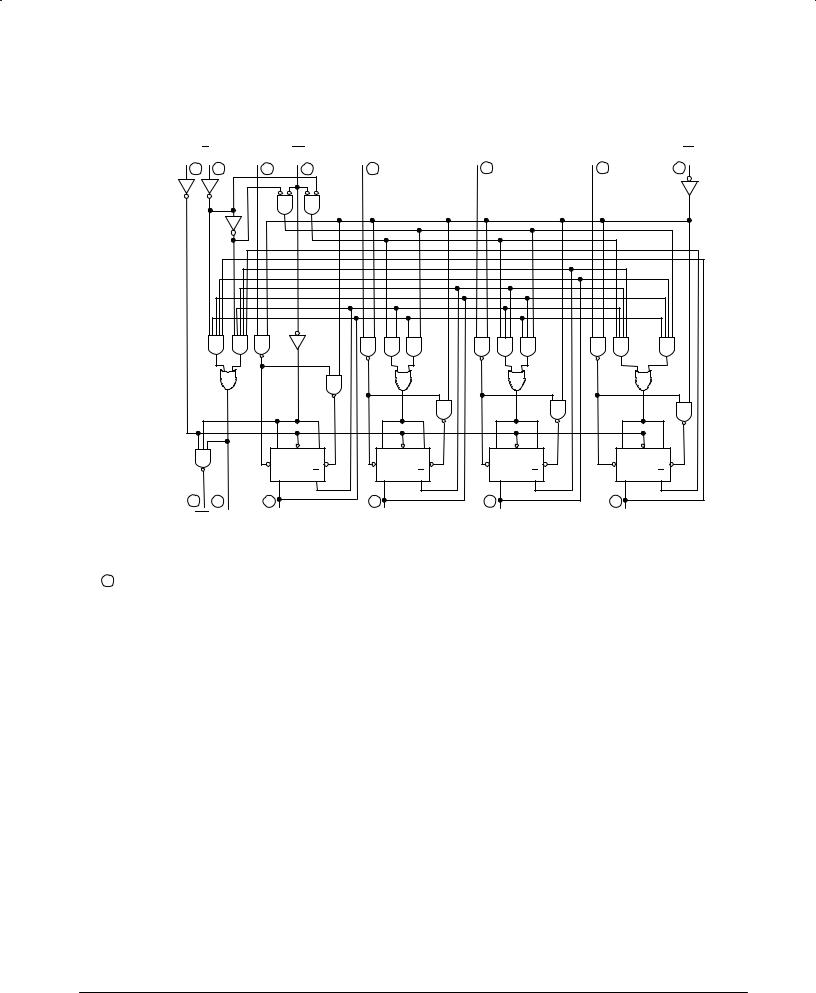
LOGIC DIAGRAMS
CP |
U/D |
P0 |
CE |
|
P1 |
|
|
P2 |
|
|
P3 |
|
PL |
|
14 |
|
5 |
15 |
4 |
|
1 |
|
|
10 |
|
|
9 |
|
11 |
|
|
|
J |
CLOCK |
K |
J |
CLOCK |
K |
J |
CLOCK |
K |
J |
CLOCK |
K |
|
|
|
PRESET CLEAR |
PRESET CLEAR |
PRESET CLEAR |
PRESET CLEAR |
||||||||
|
|
|
Q |
|
Q |
Q |
|
Q |
Q |
|
Q |
Q |
|
Q |
13 |
|
12 |
3 |
|
|
2 |
|
|
6 |
|
|
7 |
|
|
RC |
TC |
Q0 |
|
Q1 |
|
|
Q2 |
|
|
Q3 |
|
|
||
VCC = PIN 16 |
DECADE COUNTER |
|||
LS190 |
||||
GND = |
PIN |
8 |
||
= |
PIN |
NUMBERS |
|
|
FAST AND LS TTL DATA
5-342
SN54/74LS190 •SN54/74LS191
LOGIC DIAGRAMS (continued)
CP |
U/D |
P0 |
CE |
|
P1 |
|
|
P2 |
|
|
P3 |
|
PL |
|
14 |
|
5 |
15 |
4 |
|
1 |
|
|
10 |
|
|
9 |
|
11 |
|
|
|
J |
CLOCK |
K |
J |
CLOCK |
K |
J |
CLOCK |
K |
J |
CLOCK |
K |
|
|
|
PRESET CLEAR |
PRESET CLEAR |
PRESET CLEAR |
PRESET CLEAR |
||||||||
|
|
|
Q |
|
Q |
Q |
|
Q |
Q |
|
Q |
Q |
|
Q |
13 |
|
12 |
3 |
|
|
2 |
|
|
6 |
|
|
7 |
|
|
RC |
TC |
Q0 |
|
Q1 |
|
|
Q2 |
|
|
Q3 |
|
|
||
VCC = PIN 16
GND = PIN 8
= PIN NUMBERS
BINARY COUNTER
LS191
FAST AND LS TTL DATA
5-343
 Loading...