


MOTOROLA SN74LS132MR1, SN74LS132N, SN74LS132D, SN74LS132DR2, SN74LS132M Datasheet
...
SN74LS132
Quad 2-Input
Schmitt Trigger NAND Gate
The SN74LS132 contains four 2-Input NAND Gates which accept standard TTL input signals and provide standard TTL output levels. They are capable of transforming slowly changing input signals into sharply defined, jitter-free output signals. Additionally, they have greater noise margin than conventional NAND Gates.
Each circuit contains a 2-input Schmitt trigger followed by a Darlington level shifter and a phase splitter driving a TTL totem pole output. The Schmitt trigger uses positive feedback to effectively speed-up slow input transitions, and provide different input threshold voltages for positive and negative-going transitions. This hysteresis between the positive-going and negative-going input thresholds (typically 800 mV) is determined internally by resistor ratios and is essentially insensitive to temperature and supply voltage variations. As long as one input remains at a more positive voltage than VT+ (MAX), the gate will respond to the transitions of the other input as shown in Figure 1.
LOGIC AND CONNECTION DIAGRAM
DIP (TOP VIEW)
VCC
14 |
13 |
12 |
11 |
10 |
9 |
8 |
1 |
2 |
3 |
4 |
5 |
6 |
7 |
GND
GUARANTEED OPERATING RANGES
Symbol |
Parameter |
Min |
Typ |
Max |
Unit |
|
|
|
|
|
|
VCC |
Supply Voltage |
4.75 |
5.0 |
5.25 |
V |
TA |
Operating Ambient |
0 |
25 |
70 |
°C |
|
Temperature Range |
|
|
|
|
|
|
|
|
|
|
IOH |
Output Current ± High |
|
|
± 0.4 |
mA |
IOL |
Output Current ± Low |
|
|
8.0 |
mA |
http://onsemi.com
LOW
POWER
SCHOTTKY
14 
1
PLASTIC
N SUFFIX
CASE 646
14
1
SOIC
D SUFFIX
CASE 751A
ORDERING INFORMATION
Device |
Package |
Shipping |
|
|
|
SN74LS132N |
14 Pin DIP |
2000 Units/Box |
|
|
|
SN74LS132D |
14 Pin |
2500/Tape & Reel |
|
|
|
Semiconductor Components Industries, LLC, 1999 |
1 |
Publication Order Number: |
December, 1999 ± Rev. 6 |
|
SN74LS132/D |
|
|
|
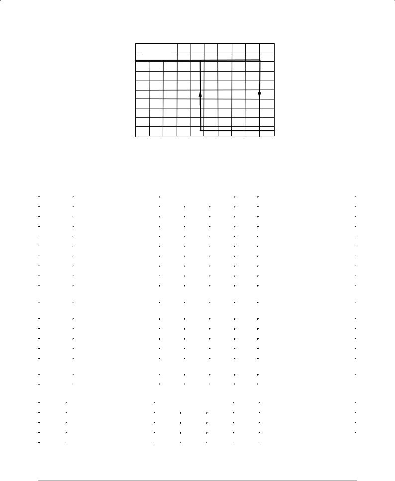
SN74LS132 |
|
|
|
|
5 |
VCC = 5 V |
|
|
|
|
(VOLTS) |
|
|
|
|
|
|
4 |
TA = 25°C |
|
|
|
|
|
|
|
|
|
|
||
|
|
|
|
|
|
|
VOLTAGE |
3 |
|
|
|
|
|
|
|
|
|
|
|
|
, OUTPUT |
2 |
|
|
|
|
|
1 |
|
|
|
|
|
|
O |
|
|
|
|
|
|
V |
|
|
|
|
|
|
|
0 0 |
0.4 |
0.95 |
1.2 |
1.8 |
2 |
VIN, INPUT VOLTAGE (VOLTS)
Figure 1. VIN versus VOUT Transfer Function
DC CHARACTERISTICS OVER OPERATING TEMPERATURE RANGE (unless otherwise specified)
|
|
|
Limits |
|
|
|
|
|
|
|
|
|
|
|
|
|
|
|
|
||
Symbol |
Parameter |
Min |
Typ |
Max |
Unit |
|
|
Test Conditions |
||
|
|
|
|
|
|
|
|
|
||
VT+ |
Positive-Going Threshold Voltage |
1.5 |
|
2.0 |
V |
VCC = 5.0 V |
|
|
||
VT± |
Negative-Going Threshold Voltage |
0.6 |
|
1.1 |
V |
VCC = 5.0 V |
|
|
||
VT + ± VT± |
Hysteresis |
0.4 |
0.8 |
|
V |
VCC = 5.0 V |
|
|
||
VIK |
Input Clamp Diode Voltage |
|
± 0.65 |
± 1.5 |
V |
VCC = MIN, IIN = ± 18 mA |
||||
VOH |
Output HIGH Voltage |
2.7 |
3.4 |
|
V |
VCC = MIN, IOH = ± 400 μA, VIN = VIL |
||||
VOL |
Output LOW Voltage |
|
0.25 |
0.4 |
V |
VCC = MIN, IOL = 4.0 mA, VIN = 2.0 V |
||||
|
0.35 |
0.5 |
V |
VCC = MIN, IOL = 8.0 mA, VIN = 2.0 V |
||||||
|
|
|
||||||||
IT+ |
Input Current at Positive-Going |
|
± 0.14 |
|
mA |
VCC = 5.0 V, VIN = VT+ |
||||
Threshold |
|
|
||||||||
IT± |
Input Current at Negative-Going |
|
± 0.18 |
|
mA |
VCC = 5.0 V, VIN = VT± |
||||
Threshold |
|
|
||||||||
IIH |
Input HIGH Current |
|
|
20 |
μA |
VCC = MAX, VIN = 2.7 V |
||||
|
|
0.1 |
mA |
VCC = MAX, VIN = 7.0 V |
||||||
|
|
|
|
|||||||
IIL |
Input LOW Current |
|
|
± 0.4 |
mA |
VCC = MAX, VIN = 0.4 V |
||||
I |
Output Short Circuit Current (1) |
± 20 |
|
±100 |
mA |
V |
CC |
= MAX, V |
OUT |
= 0 V |
OS |
|
|
|
|
|
|
|
|
||
|
Power Supply Current |
|
|
|
|
|
|
|
|
|
ICC |
Total, Output HIGH |
|
5.9 |
11 |
mA |
VCC = MAX, VIN = 0 V |
||||
|
Total, Output LOW |
|
8.2 |
14 |
mA |
VCC = MAX, VIN = 4.5 V |
||||
Note 1: Not more than one output should be shorted at a time, nor for more than 1 second.
AC CHARACTERISTICS (TA = 25°C)
|
|
|
Limits |
|
|
|
|
|
|
|
|
|
|
Symbol |
Parameter |
Min |
Typ |
Max |
Unit |
Test Conditions |
|
|
|
|
|
|
|
tPLH |
Turn-Off Delay, Input to Output |
|
|
22 |
ns |
V = 5.0 V |
|
|
|
|
|
|
CC |
tPHL |
Turn-On Delay, Input to Output |
|
|
22 |
ns |
CL = 15 pF |
http://onsemi.com
2
 Loading...