


Motorola SN54LS290J, SN54LS293J, SN74LS293N, SN74LS290N, SN74LS293D Datasheet
...SN54/74LS290
SN54/74LS293
DECADE COUNTER; 4-BIT BINARY COUNTER
The SN54/74LS290 and SN54/74LS293 are high-speed 4-bit ripple type counters partitioned into two sections. Each counter has a divide-by-two section and either a divide-by-five (LS290) or divide-by-eight (LS293) section which are triggered by a HIGH-to-LOW transition on the clock inputs. Each section can be used separately or tied together (Q to CP)to form BCD, Bi-quinary, or Modulo-16 counters. Both of the counters have a 2-input gated Master Reset (Clear), and the LS290 also has a 2-input gated Master Set (Preset 9).
•Corner Power Pin Versions of the LS90 and LS93
•Low Power Consumption . . . Typically 45 mW
•High Count Rates . . . Typically 42 MHz
•Choice of Counting Modes . . . BCD, Bi-Quinary, Binary
•Input Clamp Diodes Limit High Speed Termination Effects
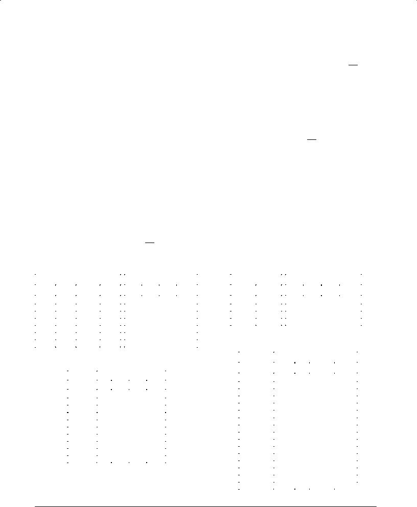
CONNECTION DIAGRAM DIP (TOP VIEW)
VCC |
MR |
|
MR |
|
CP1 |
CP0 |
Q0 |
|
Q3 |
||||||||
|
14 |
|
13 |
|
12 |
|
11 |
|
10 |
|
|
9 |
|
8 |
|
|
|
|
|
|
|
|
|
|
|
|
|
|
|
|
|
|
|
|
NOTE: |
|
|
|
|
|
|
|
|
|
|
|
|
|
|
|
|
|
|
|
|
|
|
|
|
|
|
|
|
|
|
|
|
|
|
|
The Flatpak version |
|
|
|
|
|
|
LS290 |
|
|
|
|
|
|
|
has the same pinouts |
|||
|
|
|
|
|
|
|
|
|
|
|
|
|
|
|
|
|
(Connection Diagram) as |
|
|
|
|
|
|
|
|
|
|
|
|
|
|
|
|
|
the Dual In-Line Package. |
|
|
|
|
|
|
|
|
|
|
|
|
|
|
|
|
|
|
|
1 |
|
2 |
|
3 |
|
4 |
|
|
5 |
|
|
6 |
|
7 |
|
|
|
MS |
NC |
|
MS |
|
Q2 |
Q1 |
NC |
GND |
||||||||
|
|
|
|
|
|
|
|
|
|
|
|
|
|||||
|
VCC |
MR |
|
MR |
|
CP1 |
CP0 |
Q0 |
|
Q3 |
|||||||
|
14 |
|
13 |
|
12 |
|
11 |
|
10 |
|
9 |
|
8 |
|
|
||
|
|
|
|
|
|
|
|
|
|
|
|
|
|
|
|
|
|
|
|
|
|
|
|
LS293 |
|
|
|
|
|
|
|
|
|||
|
|
|
|
|
|
|
|
|
|
|
|
|
|
||||
|
|
|
|
|
|
|
|
|
|
|
|
|
|
|
|
|
|
|
|
|
|
|
|
|
|
|
|
|
|
|
|
|
|
|
|
|
1 |
|
2 |
|
3 |
|
4 |
|
|
5 |
|
|
6 |
|
7 |
|
|
|
|
|
|
|
|
|
|
|
|
|
|
|
|
|
|
|
|
|
NC |
NC |
|
NC |
|
Q2 |
Q1 |
NC |
|
GND |
|||||||
DECADE COUNTER; 4-BIT BINARY COUNTER
LOW POWER SCHOTTKY
|
|
|
J SUFFIX |
|
|
|
CERAMIC |
|
|
|
CASE 632-08 |
14 |
1 |
|
|
|
|
|
|
|
|
|
N SUFFIX |
|
|
|
PLASTIC |
14 |
|
|
CASE 646-06 |
|
|
|
|
|
1 |
|
|
|
|
|
D SUFFIX |
|
14 |
|
SOIC |
|
|
CASE 751A-02 |
|
|
|
1 |
|
|
|
|
ORDERING INFORMATION
SN54LSXXXJ Ceramic
SN74LSXXXN Plastic
SN74LSXXXD SOIC
PIN NAMES |
|
LOADING (Note a) |
|
|||
|
|
|
HIGH |
LOW |
||
|
Clock (Active LOW going edge) Input to 2 Section. |
|
|
|
|
|
CP0 |
0.05 |
U.L. |
1.5 |
U.L. |
||
CP1 |
Clock (Active LOW going edge) Input to 5 Section (LS290). |
0.05 |
U.L. |
2.0 |
U.L. |
|
CP1 |
Clock (Active LOW going edge) Input to 8 Section (LS293). |
0.05 |
U.L. |
1.0 |
U.L. |
|
MR1, MR2 |
Master Reset (Clear) Inputs |
0.5 |
U.L. |
0.25 |
U.L. |
|
MS1, MS2 |
Master Set (Preset-9, LS290) Inputs |
0.5 |
U.L. |
0.25 |
U.L. |
|
Q0 |
Output from 2 Section (Notes b & c) |
10 |
U.L. |
5 (2.5) |
U.L. |
|
Q1, Q2, Q3 |
Outputs from 5 & 8 Sections (Note b) |
10 |
U.L. |
5 (2.5) |
U.L. |
|
|
|
|
|
|
|
|
NOTES:
a)1 TTL Unit Load (U.L.) = 40 μA HIGH/1.6 mA LOW.
b)The Output LOW drive factor is 2.5 U.L. for Military (54) and 5 U.L. for Commercial (74) Temperature Ranges.
c)The Q0 Outputs are guaranteed to drive the full fan-out plus the CP1 Input of the device.
FAST AND LS TTL DATA
5-466

SN54/74LS290 D SN54/74LS293
LOGIC SYMBOL
LS290
1 3
1 2
MS
10 CP0
CP0
11 CP1
CP1
MR Q0 Q1 Q2 Q3
1 2
12 13 9 5 4 8
VCC = PIN 14
GND = PIN 7
NC = PINS 2, 6
LS293
10 |
|
|
|
CP0 |
|
|
|
|
|
|
|
|
||
|
|
|
|
|
|
|
|
|
|
|||||
11 |
|
|
|
CP1 |
|
|
|
|
|
|
|
|
||
|
|
|
|
|
|
|
|
|
|
|
||||
|
|
|
|
MR |
Q0 Q1 Q2 Q3 |
|||||||||
|
|
|
|
1 2 |
|
|
|
|
|
|
|
|
||
|
|
|
|
|
|
|
|
|
|
|
|
|
|
|
|
|
|
|
12 13 |
9 |
5 |
4 |
8 |
||||||
VCC = PIN 14
GND = PIN 7
NC = PINS 1, 2, 3, 6
LOGIC DIAGRAMS
|
1 |
|
|
|
|
|
|
|
LS290 |
|
|
|
|
||
MS1 |
|
|
|
|
|
|
|
|
|
|
|
|
|
|
|
MS2 |
3 |
|
|
|
|
|
|
|
|
|
|
|
|
|
|
|
|
J |
SD |
J |
|
Q |
J |
|
Q |
R |
SD |
Q |
|||
|
10 |
|
|
Q |
|
|
|
|
|||||||
|
|
|
|
|
|
|
|
|
|
|
|
|
|
|
|
CP0 |
|
CP |
|
|
CP |
|
|
CP |
|
|
CP |
|
|
||
|
|
|
C |
D |
Q |
KC |
D |
Q |
KC |
D |
Q |
S C |
D |
Q |
|
|
11 |
|
|
|
VCC = PIN 14 |
|||
CP1 |
|
|
|
|
||||
|
12 |
|
|
|
GND |
= |
PIN |
7 |
MR1 |
|
9 |
5 |
4 |
8 |
= |
PIN |
NUMBERS |
MR2 |
13 |
Q0 |
Q1 |
Q2 |
Q3 |
|
|
|
|
|
|
|
|
||||
LS293
|
10 |
J |
Q |
J Q |
J Q |
J Q |
|
|
|
|
|
|
|
|
|
|
|
|
|
CP0 |
|
CP |
|
CP |
CP |
CP |
|
|
|
|
|
K CDQ |
K CDQ |
K CDQ |
K CDQ |
|
|
|
|
|
11 |
|
|
|
|
VCC = PIN 14 |
|||
CP1 |
|
|
|
|
|
||||
12 |
|
|
|
|
GND |
= |
PIN |
7 |
|
MR1 |
|
|
9 |
5 |
4 |
8 |
= |
PIN |
NUMBERS |
MR2 |
13 |
|
Q0 |
Q1 |
Q2 |
Q3 |
|
|
|
|
|
|
|
|
|
||||
FAST AND LS TTL DATA
5-467
SN54/74LS290 D SN54/74LS293
FUNCTIONAL DESCRIPTION
The LS290 and LS293 are 4-bit ripple type Decade, and 4-Bit Binary counters respectively. Each device consists of four master/slave flip-flops which are internally connected to provide a divide-by-two section and a divide-by-five (LS290) or divide-by-eight (LS293) section. Each section has a separate clock input which initiates state changes of the counter on the HIGH-to-LOW clock transition. State changes of the Q outputs do not occur simultaneously because of internal ripple delays. Therefore, decoded output signals are subject to decoding spikes and should not be used for clocks or strobes. The Q0 output of each device is designed and specified to drive the rated fan-out plus the CP1 input of the device.
A gated AND asynchronous Master Reset (MR1 MR2) is provided on both counters which overrides the clocks and resets (clears) all the flip-flops. A gated AND asynchronous Master Set (MS1 MS2) is provided on the LS290 which overrides the clocks and the MR inputs and sets the outputs to nine (HLLH).
Since the output from the divide-by-two section is not internally connected to the succeeding stages, the devices may be operated in various counting modes:
LS290
A. BCD Decade (8421) Counter Ð the CP 1 input must be
LS290 MODE SELECTION
|
RESET/SET INPUTS |
|
|
|
OUTPUTS |
|
||||
|
|
|
|
|
|
|
|
|
|
|
MR1 |
|
MR2 |
MS1 |
|
MS2 |
|
Q0 |
Q1 |
Q2 |
Q3 |
H |
|
H |
L |
|
X |
|
L |
L |
L |
L |
H |
|
H |
X |
|
L |
|
L |
L |
L |
L |
X |
|
X |
H |
|
H |
|
H |
L |
L |
H |
L |
|
X |
L |
|
X |
|
|
Count |
|
|
X |
|
L |
X |
|
L |
|
|
Count |
|
|
L |
|
X |
X |
|
L |
|
|
Count |
|
|
X |
|
L |
L |
|
X |
|
|
Count |
|
|
LS290
BCD COUNT SEQUENCE
COUNT |
|
OUTPUT |
|
||
|
|
|
|
||
Q0 |
Q1 |
Q2 |
Q3 |
||
|
|||||
0 |
L |
L |
L |
L |
|
1 |
H |
L |
L |
L |
|
2 |
L |
H |
L |
L |
|
3 |
H |
H |
L |
L |
|
4 |
L |
L |
H |
L |
|
5 |
H |
L |
H |
L |
|
6 |
L |
H |
H |
L |
|
7 |
H |
H |
H |
L |
|
8 |
L |
L |
L |
H |
|
9 |
H |
L |
L |
H |
|
NOTE: Output Q0 is connected to Input CP1 for BCD count.
H = HIGH Voltage Level
L = LOW Voltage Level
X = Don't Care
externally connected to the Q0 output. The CP0 input receives the incoming count and a BCD count sequence is produced.
B.Symmetrical Bi-quinary Divide-By-Ten Counter Ð The Q 3 output must be externally connected to the CP0 input. The input count is then applied to the CP1 input and a divide-by-ten square wave is obtained at output Q0.
C.Divide-By-Two and Divide-By-Five Counter Ð No external interconnections are required. The first flip-flop is used as a
binary element for the divide-by-two function (CP0 as the input and Q0 as the output). The CP1 input is used to obtain binary divide-by-five operation at the Q3 output.
LS293
A.4-Bit Ripple Counter Ð The output Q 0 must be externally connected to input CP1. The input count pulses are applied to input CP0. Simultaneous division of 2, 4, 8, and 16 are performed at the Q0, Q1, Q2, and Q3 outputs as shown in the truth table.
B.3-Bit Ripple Counter Ð The input count pulses are applied
to input CP1. Simultaneous frequency divisions of 2, 4, and 8 are available at the Q1, Q2, and Q3 outputs. Independent use of the first flip-flop is available if the reset function coincides with reset of the 3-bit ripple-through counter.
LS293 MODE SELECTION
RESET INPUTS |
|
|
OUTPUTS |
|
||
|
|
|
|
|
|
|
MR1 |
MR2 |
|
Q0 |
Q1 |
Q2 |
Q3 |
H |
H |
|
L |
L |
L |
L |
L |
H |
|
|
Count |
|
|
H |
L |
|
|
Count |
|
|
L |
L |
|
|
Count |
|
|
TRUTH TABLE
COUNT |
|
OUTPUT |
|
||
|
|
|
|
||
Q0 |
Q1 |
Q2 |
Q3 |
||
|
|||||
0 |
L |
L |
L |
L |
|
1 |
H |
L |
L |
L |
|
2 |
L |
H |
L |
L |
|
3 |
H |
H |
L |
L |
|
4 |
L |
L |
H |
L |
|
5 |
H |
L |
H |
L |
|
6 |
L |
H |
H |
L |
|
7 |
H |
H |
H |
L |
|
8 |
L |
L |
L |
H |
|
9 |
H |
L |
L |
H |
|
10 |
L |
H |
L |
H |
|
11 |
H |
H |
L |
H |
|
12 |
L |
L |
H |
H |
|
13 |
H |
L |
H |
H |
|
14 |
L |
H |
H |
H |
|
15 |
H |
H |
H |
H |
|
Note: Output Q0 connected to input CP1.
FAST AND LS TTL DATA
5-468
 Loading...