


MOTOROLA SN74LS151M, SN74LS151MEL, SN74LS151ML1, SN74LS151ML2, SN74LS151MR1 Datasheet
...SN74LS151
8-Input Multiplexer
The TTL / MSI SN74LS151 is a high speed 8-input Digital Multiplexer. It provides, in one package, the ability to select one bit of data from up to eight sources. The LS151 can be used as a universal function generator to generate any logic function of four variables. Both assertion and negation outputs are provided.
•Schottky Process for High Speed
•Multifunction Capability
•On-Chip Select Logic Decoding
•Fully Buffered Complementary Outputs
•Input Clamp Diodes Limit High Speed Termination Effects
GUARANTEED OPERATING RANGES
Symbol |
Parameter |
Min |
Typ |
Max |
Unit |
|
|
|
|
|
|
VCC |
Supply Voltage |
4.75 |
5.0 |
5.25 |
V |
TA |
Operating Ambient |
0 |
25 |
70 |
°C |
|
Temperature Range |
|
|
|
|
|
|
|
|
|
|
IOH |
Output Current ± High |
|
|
± 0.4 |
mA |
IOL |
Output Current ± Low |
|
|
8.0 |
mA |
http://onsemi.com
LOW
POWER
SCHOTTKY
16
1
PLASTIC
N SUFFIX
CASE 648
16
1
SOIC
D SUFFIX
CASE 751B
ORDERING INFORMATION
Device |
Package |
Shipping |
|
|
|
SN74LS151N |
16 Pin DIP |
2000 Units/Box |
|
|
|
SN74LS151D |
16 Pin |
2500/Tape & Reel |
|
|
|
Semiconductor Components Industries, LLC, 1999 |
1 |
Publication Order Number: |
December, 1999 ± Rev. 6 |
|
SN74LS151/D |
SN74LS151
CONNECTION DIAGRAM DIP (TOP VIEW)
VCC |
|
I4 |
I5 |
|
I6 |
|
I7 |
|
S0 |
|
S1 |
|
S2 |
|
16 |
|
15 |
|
14 |
|
13 |
|
12 |
|
11 |
|
10 |
|
9 |
|
1 |
|
2 |
|
|
3 |
|
|
4 |
|
5 |
|
6 |
|
7 |
|
|
8 |
|
|
||||||
|
|
|
I3 |
I2 |
|
|
I1 |
I0 |
Z |
|
|
|
|
|
|
GND |
|
|||||||||
|
|
|
|
|
Z |
E |
|
|||||||||||||||||||
|
|
|
|
|
|
|
|
|
|
|
|
|
|
|
|
|
|
|
|
|
|
|
LOADING (Note a) |
|||
|
|
|
|
|
|
|
|
|
|
|
|
|
|
|
|
|
|
|
|
|
|
|
|
|
||
PIN NAMES |
|
|
|
|
|
|
|
|
|
|
|
|
|
|
|
|
|
|
HIGH |
LOW |
||||||
S0 ± S2 |
|
Select Inputs |
|
|
|
|
|
|
|
|
|
|
|
|
0.5 U.L. |
0.25 U.L. |
||||||||||
E |
|
|
|
|
Enable (Active LOW) Input |
|
|
|
|
|
|
|
|
0.5 U.L. |
0.25 U.L. |
|||||||||||
I0 ± I7 |
|
Multiplexer Inputs |
|
|
|
|
|
|
|
|
|
|
0.5 U.L. |
0.25 U.L. |
||||||||||||
Z |
|
Multiplexer Output |
|
|
|
|
|
|
|
|
|
|
10 U.L. |
5 U.L. |
||||||||||||
|
|
|
|
|
Complementary Multiplexer Output |
|
|
|
|
10 U.L. |
5 U.L. |
|||||||||||||||
Z |
|
|
|
|
|
|||||||||||||||||||||
NOTES:
a)1 TTL Unit Load (U.L.) = 40 mA HIGH/1.6 mA LOW.
b)The Output LOW drive factor is 5 U.L. for Commercial (74) Temperature Ranges.
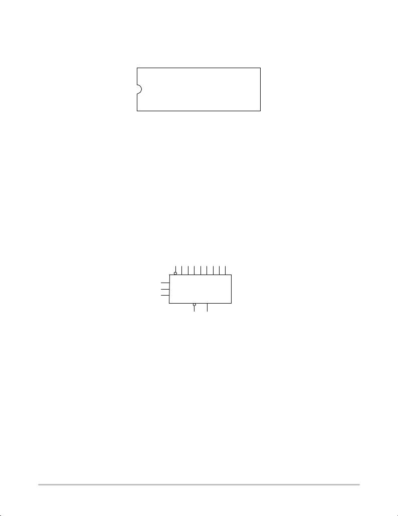
LOGIC SYMBOL
|
7 |
4 |
3 |
2 |
1 15 14 13 12 |
|
11 |
E I0 I1 I2 I3 I4 I5 I6 I7 |
|||||
S0 |
|
|
|
|
|
|
10 |
S1 |
|
|
|
|
|
9 |
S2 |
|
|
|
|
|
|
|
Z |
Z |
|||
|
|
|
|
|||
|
|
|
|
6 |
5 |
|
VCC = PIN 16
GND = PIN 8
http://onsemi.com
2

|
SN74LS151 |
|
|
|
|
|
||
LOGIC DIAGRAM |
|
|
|
|
|
|||
I0 |
I1 |
|
I2 |
I3 |
I4 |
I5 |
I6 |
I7 |
9 |
4 |
3 |
2 |
1 |
15 |
14 |
13 |
12 |
S2 
10
S1 
11
S0 
7
E 
VCC = PIN 16 |
|
|
GND = PIN 8 |
|
6 5 |
= PIN NUMBERS |
Z |
Z |
|
FUNCTIONAL DESCRIPTION
The LS151 is a logical implementation of a single pole, 8-position switch with the switch position controlled by the state of three Select inputs, S0, S1, S2. Both assertion and negation outputs are provided. The Enable input (E) is active LOW. When it is not activated, the negation output is HIGH and the assertion output is LOW regardless of all other inputs. The logic function provided at the output is:
Z= E (I0 S0 S1 S2 + I1 S0 S1 S2 + I2 S0 S1 S2
+I3 S0 S1 S2 + I4 S0 S1 S2 + I5 S0 S1 S2 + I6
S1 S2 + I7 S0 S1 S2).S0
The LS151 provides the ability, in one package, to select from eight sources of data or control information. By proper manipulation of the inputs, the LS151 can provide any logic function of four variables and its negation.
TRUTH TABLE
|
|
|
|
|
|
|
|
|
|
|
|
|
E |
S2 S1 S0 |
|
I0 |
I1 |
I2 |
I3 I4 I5 I6 I7 |
Z Z |
|||
H |
X X X |
X X X X X X X X |
H L |
||||||||
|
L |
L L L |
L |
X X X X X X X |
H L |
||||||
|
L |
L L L |
H X X X X X X X |
L H |
|||||||
|
L |
L L H |
X L |
X X X X X X |
H L |
||||||
|
L |
L L H |
|
X H X X X X X X |
L H |
||||||
|
L |
L H L |
X X L |
X X X X X |
H L |
||||||
|
L |
L H L |
|
X X H X X X X X |
L H |
||||||
|
L |
L H H |
X X X L X X X X |
H L |
|||||||
|
L |
L H H |
|
X X X H X X X X |
L H |
||||||
|
L |
H L L |
X X X X L X X X |
H L |
|||||||
|
L |
H L L |
|
X X X X H X X X |
L H |
||||||
|
L |
H L H |
X X X X X L X X |
H L |
|||||||
|
L |
H L H |
|
X X X X X H X X |
L H |
||||||
|
L |
H H L |
X X X X X X L X |
H L |
|||||||
|
L |
H H L |
X X X X X X H X |
L H |
|||||||
|
L |
H H H |
X X X X X X X L |
H L |
|||||||
|
L |
H H H |
X X X X X X X H |
L H |
|||||||
|
|
|
|
|
|
|
|
|
|
||
H = HIGH Voltage Level |
|
|
|
|
|
|
|
||||
L = LOW Voltage Level |
|
|
|
|
|
|
|
||||
X = Don't Care |
|
|
|
|
|
|
|
||||
http://onsemi.com
3
 Loading...