


MOTOROLA MC74VHC374ML1, MC74VHC374DWR2, MC74VHC374M, MC74VHC374MEL, MC74VHC374DTR2 Datasheet
...
MOTOROLA
SEMICONDUCTOR TECHNICAL DATA
Octal D-Type Flip-Flop with 3-State Output
The MC74VHC374 is an advanced high speed CMOS octal flip±flip with 3±state output fabricated with silicon gate CMOS technology. It achieves high speed operation similar to equivalent Bipolar Schottky TTL while maintaining CMOS low power dissipation.
This 8±bit D±type flip±flop is controlled by a clock input and an output enable input. When the output enable input is high, the eight outputs are in a high impedance state.
The internal circuit is composed of three stages, including a buffer output which provides high noise immunity and stable output. The inputs tolerate voltages up to 7V, allowing the interface of 5V systems to 3V systems.
•High Speed: fmax = 185MHz (Typ) at VCC = 5V
•Low Power Dissipation: ICC = 4μA (Max) at TA = 25°C
•High Noise Immunity: VNIH = VNIL = 28% VCC
•Power Down Protection Provided on Inputs
•Balanced Propagation Delays
•Designed for 2V to 5.5V Operating Range
•Low Noise: VOLP = 0.9V (Max)
•Pin and Function Compatible with Other Standard Logic Families
•Latchup Performance Exceeds 300mA
•ESD Performance: HBM > 2000V; Machine Model > 200V
•Chip Complexity: 266 FETs or 66.5 Equivalent Gates
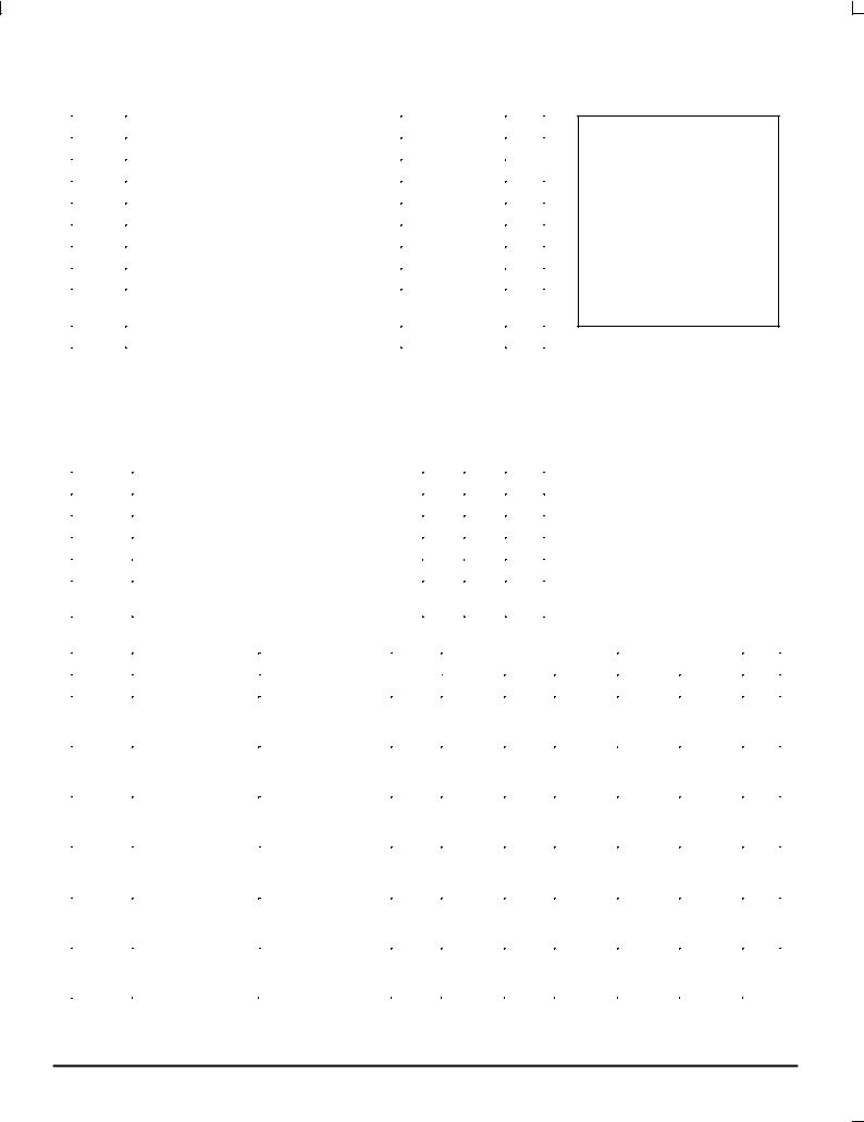
LOGIC DIAGRAM
|
|
|
D0 |
3 |
|
|
2 |
Q0 |
|
|
|
|
|
4 |
|
|
5 |
|
|||
|
|
|
D1 |
|
|
Q1 |
|
|||
|
|
|
7 |
|
|
6 |
|
|||
|
|
|
D2 |
|
|
Q2 |
|
|||
DATA |
|
|
8 |
|
|
9 |
|
|||
|
|
|
|
|
|
|
||||
|
D3 |
|
|
Q3 |
NONINVERTING |
|||||
|
|
|
|
|||||||
INPUTS |
|
|
13 |
|
|
12 |
|
|||
D4 |
|
|
Q4 |
OUTPUTS |
||||||
|
|
|
|
|
||||||
|
|
|
14 |
|
|
15 |
|
|||
|
|
|
D5 |
|
|
Q5 |
|
|||
|
|
|
17 |
|
|
16 |
|
|||
|
|
|
D6 |
|
|
Q6 |
|
|||
|
|
|
18 |
|
|
19 |
|
|||
|
|
|
D7 |
|
|
|
|
|||
|
|
|
|
|
Q7 |
|
||||
|
|
|
11 |
|
|
|
|
|||
|
|
|
CP |
|
|
|
|
|
||
|
|
|
1 |
|
|
|
|
|
||
|
|
|
|
|
|
|
|
|
|
|
|
|
|
|
|
|
|
|
|
|
|
|
|
|
OE |
|
|
|
|
|
||
|
|
|
|
|
|
|
|
|
||
FUNCTION TABLE
|
|
|
INPUTS |
|
OUTPUT |
||||
|
|
|
|
|
|
|
|
|
|
|
OE |
|
CP |
D |
Q |
||||
|
|
|
|
|
|
|
|
|
|
|
L |
|
|
|
|
|
|
H |
H |
|
|
|
|
|
|
|
|||
|
L |
|
|
|
|
|
|
L |
L |
|
L |
|
L, H, |
|
|
X |
No Change |
||
|
H |
|
|
X |
X |
Z |
|||
|
|
|
|
|
|
|
|
|
|
MC74VHC374
DW SUFFIX
20±LEAD SOIC PACKAGE
CASE 751D±04
DT SUFFIX
20±LEAD TSSOP PACKAGE
CASE 948E±02
M SUFFIX
20±LEAD SOIC EIAJ PACKAGE
CASE 967±01
ORDERING INFORMATION
MC74VHCXXXDW SOIC MC74VHCXXXDT TSSOP MC74VHCXXXM SOIC EIAJ
PIN ASSIGNMENT
|
|
|
1 |
20 |
VCC |
|
OE |
||||
|
Q0 |
2 |
19 |
Q7 |
|
|
D0 |
3 |
18 |
D7 |
|
|
D1 |
4 |
17 |
D6 |
|
|
Q1 |
5 |
16 |
Q6 |
|
|
Q2 |
6 |
15 |
Q5 |
|
|
D2 |
7 |
14 |
D5 |
|
|
D3 |
8 |
13 |
D4 |
|
|
Q3 |
9 |
12 |
Q4 |
|
GND |
10 |
11 |
CP |
||
|
|
|
|
|
|
6/97
Motorola, Inc. 1997 |
1 |
REV 1 |
MC74VHC374
MAXIMUM RATINGS*
Symbol |
Parameter |
|
Value |
Unit |
|
|
|
|
|
VCC |
DC Supply Voltage |
|
± 0.5 to + 7.0 |
V |
Vin |
DC Input Voltage |
|
± 0.5 to + 7.0 |
V |
Vout |
DC Output Voltage |
|
± 0.5 to VCC + 0.5 |
V |
IIK |
Input Diode Current |
|
± 20 |
mA |
IOK |
Output Diode Current |
|
± 20 |
mA |
Iout |
DC Output Current, per Pin |
|
± 25 |
mA |
ICC |
DC Supply Current, VCC and GND Pins |
± 75 |
mA |
|
PD |
Power Dissipation in Still Air, |
SOIC Packages² |
500 |
mW |
|
|
TSSOP Package² |
450 |
|
|
|
|
|
|
Tstg |
Storage Temperature |
|
± 65 to + 150 |
_C |
*Absolute maximum continuous ratings are those values beyond which damage to the device may occur. Exposure to these conditions or conditions beyond those indicated may adversely affect device reliability. Functional operation under absolute±maximum±rated conditions is not implied.
²Derating Ð SOIC Packages: ± 7 mW/ _C from 65_ to 125_C TSSOP Package: ± 6.1 mW/_C from 65_ to 125_C
RECOMMENDED OPERATING CONDITIONS
Symbol |
Parameter |
|
Min |
Max |
Unit |
|
|
|
|
|
|
VCC |
DC Supply Voltage |
|
2.0 |
5.5 |
V |
Vin |
DC Input Voltage |
|
0 |
5.5 |
V |
Vout |
DC Output Voltage |
|
0 |
VCC |
V |
TA |
Operating Temperature |
|
± 40 |
+ 85 |
_C |
tr, tf |
Input Rise and Fall Time |
VCC = 3.3V |
0 |
100 |
ns/V |
|
|
VCC = 5.0V |
0 |
20 |
|
DC ELECTRICAL CHARACTERISTICS
This device contains protection circuitry to guard against damage due to high static voltages or electric fields. However, precautions must be taken to avoid applications of any voltage higher than maximum rated voltages to this high±impedance circuit. For proper operation, Vin and Vout should be constrained to the
range GND v (Vin or Vout) v VCC. Unused inputs must always be
tied to an appropriate logic voltage level (e.g., either GND or VCC). Unused outputs must be left open.
|
|
|
VCC |
|
TA = 25°C |
|
TA = ± 40 to 85°C |
|
|
Symbol |
Parameter |
Test Conditions |
V |
Min |
Typ |
Max |
Min |
Max |
Unit |
|
|
|
|
|
|
|
|
|
|
VIH |
Minimum High±Level |
|
2.0 |
1.50 |
|
|
1.50 |
|
V |
|
Input Voltage |
|
3.0 to |
VCC x 0.7 |
|
|
VCC x 0.7 |
|
|
|
|
|
5.5 |
|
|
|
|
|
|
|
|
|
|
|
|
|
|
|
|
VIL |
Maximum Low±Level |
|
2.0 |
|
|
0.50 |
|
0.50 |
V |
|
Input Voltage |
|
3.0 to |
|
|
VCC x 0.3 |
|
VCC x 0.3 |
|
|
|
|
5.5 |
|
|
|
|
|
|
|
|
|
|
|
|
|
|
|
|
VOH |
Minimum High±Level |
Vin = VIH or VIL |
2.0 |
1.9 |
2.0 |
|
1.9 |
|
V |
|
Output Voltage |
IOH = ± 50μA |
3.0 |
2.9 |
3.0 |
|
2.9 |
|
|
|
|
|
4.5 |
4.4 |
4.5 |
|
4.4 |
|
|
|
|
|
|
|
|
|
|
|
|
|
|
Vin = VIH or VIL |
|
|
|
|
|
|
|
|
|
IOH = ± 4mA |
3.0 |
2.58 |
|
|
2.48 |
|
|
|
|
IOH = ± 8mA |
4.5 |
3.94 |
|
|
3.80 |
|
|
VOL |
Maximum Low±Level |
Vin = VIH or VIL |
2.0 |
|
0.0 |
0.1 |
|
0.1 |
V |
|
Output Voltage |
IOL = 50μA |
3.0 |
|
0.0 |
0.1 |
|
0.1 |
|
|
|
|
4.5 |
|
0.0 |
0.1 |
|
0.1 |
|
|
|
|
|
|
|
|
|
|
|
|
|
Vin = VIH or VIL |
|
|
|
|
|
|
|
|
|
IOL = 4mA |
3.0 |
|
|
0.36 |
|
0.44 |
|
|
|
IOL = 8mA |
4.5 |
|
|
0.36 |
|
0.44 |
|
MOTOROLA |
2 |
VHC Data ± Advanced CMOS Logic |
|
|
DL203 Ð Rev 1 |
MC74VHC374
DC ELECTRICAL CHARACTERISTICS
|
|
|
VCC |
|
TA = 25°C |
|
TA = ± 40 to 85°C |
|
|
Symbol |
Parameter |
Test Conditions |
V |
Min |
Typ |
Max |
Min |
Max |
Unit |
|
|
|
|
|
|
|
|
|
|
Iin |
Maximum Input |
Vin = 5.5V or GND |
0 to 5.5 |
|
|
± 0.1 |
|
± 1.0 |
μA |
|
Leakage Current |
|
|
|
|
|
|
|
|
|
|
|
|
|
|
|
|
|
|
IOZ |
Maximum Three±State |
Vin = VIL or VIH |
5.5 |
|
|
± 0.25 |
|
± 2.5 |
μA |
|
Leakage Current |
Vout = VCC or GND |
|
|
|
|
|
|
|
ICC |
Maximum Quiescent |
Vin = VCC or GND |
5.5 |
|
|
4.0 |
|
40.0 |
μA |
|
Supply Current |
|
|
|
|
|
|
|
|
|
|
|
|
|
|
|
|
|
|
AC ELECTRICAL CHARACTERISTICS (Input tr = tf = 3.0ns)
|
|
|
|
|
|
TA = 25°C |
|
|
TA = ± 40 to 85°C |
|
|||
Symbol |
|
Parameter |
Test Conditions |
Min |
Typ |
Max |
|
Min |
Max |
Unit |
|||
|
|
|
|
|
|
|
|
|
|
|
|
|
|
fmax |
|
Maximum Clock Frequency |
VCC = 3.3 ± 0.3V |
CL = 15pF |
80 |
130 |
|
|
70 |
|
|
ns |
|
|
|
(50% Duty Cycle) |
|
CL = 50pF |
55 |
85 |
|
|
50 |
|
|
|
|
|
|
|
VCC = 5.0 ± 0.5V |
CL = 15pF |
130 |
185 |
|
|
110 |
|
|
|
|
|
|
|
|
CL = 50pF |
85 |
120 |
|
|
75 |
|
|
|
|
tPLH, |
|
Maximum Propagation Delay, |
VCC = 3.3 ± 0.3V |
CL = 15pF |
|
8.1 |
12.7 |
|
1.0 |
15.0 |
|
ns |
|
tPHL |
|
CP to Q |
|
CL = 50pF |
|
10.6 |
16.2 |
|
1.0 |
18.5 |
|
|
|
|
|
|
VCC = 5.0 ± 0.5V |
CL = 15pF |
|
5.4 |
8.1 |
|
1.0 |
9.5 |
|
|
|
|
|
|
|
CL = 50pF |
|
6.9 |
10.1 |
|
1.0 |
11.5 |
|
|
|
tPZL, |
|
Output Enable Time, |
VCC = 3.3 ± 0.3V |
CL = 15pF |
|
7.1 |
11.0 |
|
1.0 |
13.0 |
|
ns |
|
tPZH |
|
OE to Q |
RL = 1kΩ |
CL = 50pF |
|
9.6 |
14.5 |
|
1.0 |
16.5 |
|
|
|
|
|
|
VCC = 5.0 ± 0.5V |
CL = 15pF |
|
5.1 |
7.6 |
|
1.0 |
9.0 |
|
|
|
|
|
|
RL = 1kΩ |
CL = 50pF |
|
6.6 |
9.6 |
|
1.0 |
11.0 |
|
|
|
tPLZ, |
|
Output Disable Time, |
VCC = 3.3 ± 0.3V |
CL = 50pF |
|
10.2 |
14.0 |
|
1.0 |
16.0 |
|
ns |
|
tPHZ |
|
OE to Q |
RL = 1kΩ |
|
|
|
|
|
|
|
|
|
|
|
|
|
VCC = 5.0 ± 0.5V |
CL = 50pF |
|
6.1 |
8.8 |
|
1.0 |
10.0 |
|
|
|
|
|
|
RL = 1kΩ |
|
|
|
|
|
|
|
|
|
|
tOSLH, |
|
Output to Output Skew |
VCC = 3.3 ± 0.3V |
CL = 50pF |
|
|
|
1.5 |
|
|
1.5 |
|
pF |
tOSHL |
|
|
(Note 1.) |
|
|
|
|
|
|
|
|
|
|
|
|
|
VCC = 5.0 ± 0.5V |
CL = 50pF |
|
|
|
1.0 |
|
|
1.0 |
|
pF |
|
|
|
(Note 1.) |
|
|
|
|
|
|
|
|
|
|
|
|
|
|
|
|
|
|
|
|
|
|
|
|
Cin |
|
Maximum Input Capacitance |
|
|
|
4 |
10 |
|
|
10 |
|
pF |
|
Cout |
|
Maximum Three±State Output |
|
|
|
6 |
|
|
|
|
|
pF |
|
|
|
Capacitance (Output in |
|
|
|
|
|
|
|
|
|
|
|
|
|
High±Impedance State) |
|
|
|
|
|
|
|
|
|
|
|
|
|
|
|
|
|
|
|
|
|
|
|
|
|
|
|
|
|
|
|
|
|
|
|
||||
|
|
|
|
|
|
|
Typical @ 25°C, VCC = 5.0V |
|
|
||||
CPD |
|
Power Dissipation Capacitance (Note 2.) |
|
|
|
|
|
32 |
|
|
pF |
||
1.Parameter guaranteed by design. tOSLH = |tPLHm ± tPLHn|, tOSHL = |tPHLm ± tPHLn|.
2.CPD is defined as the value of the internal equivalent capacitance which is calculated from the operating current consumption without load.
Average operating current can be obtained by the equation: ICC(OPR) = CPD VCC fin + ICC / 8 (per flip±flop). CPD is used to determine the no±load dynamic power consumption; PD = CPD VCC2 fin + ICC VCC.
VHC Data ± Advanced CMOS Logic |
3 |
MOTOROLA |
DL203 Ð Rev 1 |
|
|
 Loading...