


MOTOROLA MC74VHC139DT, MC74VHC139DTEL, MC74VHC139DTR2, MC74VHC139DR2, MC74VHC139ML2 Datasheet
...
MOTOROLA
SEMICONDUCTOR TECHNICAL DATA
Dual 2-to-4 Decoder/
Demultiplexer
The MC74VHC139 is an advanced high speed CMOS 2±to±4 decoder/ demultiplexer fabricated with silicon gate CMOS technology. It achieves high speed operation similar to equivalent Bipolar Schottky TTL while maintaining CMOS low power dissipation.
When the device is enabled (E = low), it can be used for gating or as a data input for demultiplexing operations. When the enable input is held high, all four outputs are fixed high, independent of other inputs.
The internal circuit is composed of three stages, including a buffer output which provides high noise immunity and stable output. The inputs tolerate voltages up to 7V, allowing the interface of 5V systems to 3V systems.
•High Speed: tPD = 5.0ns (Typ) at VCC = 5V
•Low Power Dissipation: ICC = 4μΑ (Max) at TA = 25°C
•High Noise Immunity: VNIH = VNIL = 28% VCC
•Power Down Protection Provided on Inputs
•Balanced Propagation Delays
•Designed for 2V to 5.5V Operating Range
•Low Noise: VOLP = 0.8 V (Max)
•Pin and Function Compatible with Other Standard Logic Families
•Latchup Performance Exceeds 300mA
•ESD Performance: HBM > 2000V; Machine Model > 200V
•Chip Complexity: 100 FETs or 25 Equivalent Gates
LOGIC DIAGRAM
ADDRESS |
A0a |
2 |
4 |
Y0a |
|
|
|
|
|||
INPUTS |
A1a |
3 |
5 |
Y1a |
ACTIVE±LOW |
|
|
6 |
|||
|
|
|
Y2a |
OUTPUTS |
|
|
|
|
|
||
|
|
|
|
|
|
|
|
|
7 |
Y3a |
|
|
|
|
|
|
|
|
Ea |
1 |
|
|
|
|
|
|
|
|
|
ADDRESS |
A0b |
14 |
12 |
Y0b |
|
INPUTS |
A1b |
13 |
11 |
Y1b |
ACTIVE±LOW |
|
|
|
10 |
Y2b |
OUTPUTS |
|
|
|
|
|
|
|
|
|
9 |
Y3b |
|
|
|
|
|
|
|
|
Eb |
15 |
|
|
|
MC74VHC139
D SUFFIX
16±LEAD SOIC PACKAGE
CASE 751B±05
DT SUFFIX
16±LEAD TSSOP PACKAGE
CASE 948F±01
M SUFFIX
16±LEAD SOIC EIAJ PACKAGE
CASE 966±01
ORDERING INFORMATION
MC74VHCXXXD SOIC MC74VHCXXXDT TSSOP MC74VHCXXXM SOIC EIAJ
PIN ASSIGNMENT
|
|
|
|
|
|
|
|
|
|
|
|
|
Ea |
|
1 |
16 |
|
VCC |
|||
|
|
|
|
|||||||
|
|
|
||||||||
|
|
|
|
|
2 |
15 |
|
|
|
|
|
A0a |
|
Eb |
|||||||
|
|
|||||||||
|
||||||||||
|
|
|
3 |
14 |
|
|
|
|
||
|
A1a |
|
A0b |
|||||||
|
||||||||||
|
|
|
|
4 |
13 |
|
|
|
|
|
Y0a |
|
A1b |
||||||||
|
||||||||||
|
|
|
|
|
|
|
|
|
||
|
Y1a |
|
5 |
12 |
|
Y0b |
||||
|
||||||||||
|
|
|
|
|
|
|
|
|
|
|
|
Y2a |
|
6 |
11 |
|
|
|
|
||
|
|
|
Y1b |
|||||||
|
|
|||||||||
|
|
|
|
|
|
|
|
|
|
|
|
|
|
|
|
7 |
10 |
|
Y2b |
||
|
Y3a |
|
|
|||||||
|
|
|||||||||
|
||||||||||
|
|
|
|
|
|
|
|
|||
GND |
|
8 |
9 |
|
Y3b |
|||||
|
|
|||||||||
|
||||||||||
|
|
|
|
|
|
|
|
|
|
|
FUNCTION TABLE
|
Inputs |
|
|
Outputs |
|
|
|
|
|
|
|
|
|
E |
A1 |
A0 |
Y0 |
Y1 |
Y2 |
Y3 |
|
|
|
|
|
|
|
H |
X |
X |
H |
H |
H |
H |
L |
L |
L |
L |
H |
H |
H |
L |
L |
H |
H |
L |
H |
H |
L |
H |
L |
H |
H |
L |
H |
L |
H |
H |
H |
H |
H |
L |
|
|
|
|
|
|
|
6/97
Motorola, Inc. 1997 |
1 |
REV 0 |
MC74VHC139
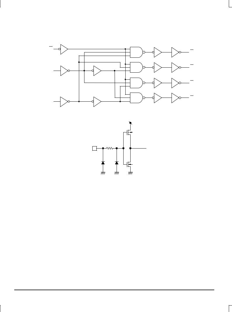
EXPANDED LOGIC DIAGRAM
(1/2 OF DEVICE)
En |
Y0 |
Y1 |
A0 |
Y2 |
Y3 |
A1 |
INPUT
Figure 1. Input Equivalent Circuit
MOTOROLA |
2 |
VHC Data ± Advanced CMOS Logic |
|
|
DL203 Ð Rev 0 |
 Loading...