


Order this document by MC75172B/D
MC75172B Quad EIA-485 Line Drivers MC75174B with Three-State Outputs
The Motorola MC75172B/174B Quad Line drivers are differential high |
|
|
|
speed drivers designed to comply with the EIA±485 Standard. Features |
QUAD EIA±485 LINE DRIVERS |
||
include three±state outputs, thermal shutdown, and output current limiting in |
|||
both directions. These devices also comply with EIA±422±A, and CCITT |
|
|
|
Recommendations V.11 and X.27. |
SEMICONDUCTOR |
|
|
The MC75172B/174B are optimized for balanced multipoint bus |
|
||
TECHNICAL DATA |
|
||
transmission at rates in excess of 10 MBPS. The outputs feature wide |
|
||
|
|
|
|
common mode voltage range, making them suitable for party line |
|
|
|
applications in noisy environments. The current limit and thermal shutdown |
|
|
|
features protect the devices from line fault conditions. These devices offer |
|
|
|
optimum performance when used with the MC75173 and MC75175 line |
|
|
|
receivers. |
|
P SUFFIX |
|
Both devices are available in 16±pin plastic DIP and 20±pin wide body |
|
||
|
PLASTIC PACKAGE |
||
surface mount packages. |
|
CASE 648 |
|
• Meets EIA±485 Standard for Party Line Operation |
|
|
|
• Meets EIA±422±A and CCITT Recommendations V.11 and X.27 |
|
|
|
• Operating Ambient Temperature: ±40°C to +85°C |
DW SUFFIX |
|
|
• High Impedance Outputs |
|
||
PLASTIC PACKAGE |
|
||
• Common Mode Output Voltage Range: ±7 to 12 V |
CASE 751D |
|
|
• Positive and Negative Current Limiting |
(SO±20L) |
|
|
|
|
|
|
• Transmission Rates in Excess of 10 MBPS |
|
|
|
• Thermal Shutdown at 150°C Junction Temperature, (± 20°C) |
ORDERING INFORMATION |
||
• Single 5.0 V Supply |
|
Operating |
|
• Pin Compatible with TI SN75172/4 and NS μA96172/4 |
Device |
Temperature Range |
Package |
|
|
|
|
• Interchangeable with MC3487 and AM26LS31 for EIA±422±A |
MC75172BDW |
|
SO±20L |
Applications |
MC75174BDW |
TA = ± 40° to +85°C |
SO±20L |
|
|
|
|
|
|
|
|
|
|
MC75174BP |
|
|
Plastic DIP |
|||
|
|
|
|
|
|
PIN CONNECTIONS |
|
|
|
|
|
|
||||
|
|
MC75172B |
|
|
|
|
MC75174B |
|
|
|||||||
1A |
1 |
16 |
VCC |
1A |
1 |
20 |
VCC |
1A |
1 |
16 |
VCC 1A |
1 |
20 |
VCC |
||
1Y |
2 |
15 |
4A |
1Y |
2 |
19 |
4A |
1Y |
2 |
15 |
4A |
1Y |
2 |
19 |
4A |
|
1Z |
3 |
14 |
4Y |
NC |
3 |
18 |
4Y |
1Z |
3 |
14 |
4Y |
NC |
3 |
18 |
4Y |
|
En |
4 |
13 |
4Z |
1Z |
4 |
17 |
NC |
En |
4 |
13 |
4Z |
1Z |
4 |
17 |
NC |
|
2Z |
5 |
12 |
En |
En |
5 |
16 |
4Z |
12 |
|
|
En |
En |
5 |
16 |
4Z |
|
2Z |
5 |
12 |
||||||||||||||
|
|
|
|
2Z |
6 |
15 |
En |
|
|
|
34 |
12 |
|
|
En |
|
|
6 |
11 |
|
|
|
|
2Z |
6 |
15 |
|||||||
2Y |
3Z |
2Y |
6 |
11 |
3Z |
|||||||||||
34 |
||||||||||||||||
2A |
7 |
10 |
3Y |
NC |
7 |
14 |
3Z |
2A |
7 |
10 |
3Y |
NC |
7 |
14 |
3Z |
|
Gnd |
8 |
9 |
3A |
2Y |
8 |
13 |
NC |
Gnd |
8 |
9 |
3A |
2Y |
8 |
13 |
NC |
|
|
|
|
|
|
|
|
|
|||||||||
|
|
P Package |
|
2A |
9 |
12 |
3Y |
|
|
P Package |
|
2A |
9 |
12 |
3Y |
|
|
|
|
Gnd 10 |
11 |
3A |
|
|
|
Gnd 10 |
11 |
3A |
|||||
|
|
|
|
|
|
|
|
|||||||||
|
|
|
|
|
|
DW Package |
|
|
|
|
|
|
|
DW Package |
|
|
Motorola, Inc. 1996 |
Rev 1 |
MC75172B MC75174B
MAXIMUM RATINGS
Rating |
Symbol |
Value |
Unit |
|
|
|
|
Power Supply Voltage |
VCC |
±0.5, +7.0 |
Vdc |
Input Voltage (Data, Enable) |
Vin |
+7.0 |
Vdc |
Input Current (Data, Enable) |
Iin |
±24 |
mA |
Applied Output Voltage, when in 3±State Condition |
Vza |
±10, +14 |
Vdc |
(VCC = 5.0 V) |
|
|
|
Applied Output Voltage, when VCC = 0 V |
Vzb |
±14 |
|
Output Current |
IO |
Self±Limiting |
± |
Storage Temperature |
Tstg |
±65, +150 |
°C |
Devices should not be operated at these limits. The ªRecommended Operating Conditionsº table provides |
|||
for actual device operation. |
|
|
|
RECOMMENDED OPERATING CONDITIONS
Characteristic |
Symbol |
Min |
Typ |
Max |
Unit |
|
|
|
|
|
|
Power Supply Voltage |
VCC |
+4.75 |
+5.0 |
+5.25 |
Vdc |
Input Voltage (All Inputs) |
Vin |
0 |
± |
VCC |
Vdc |
Output Voltage in 3±State Condition, or when VCC = 0 V |
Vcm |
±7.0 |
± |
+12 |
Vdc |
Output Current (Normal data transmission) |
IO |
±65 |
± |
+65 |
mA |
Operating Ambient Temperature (see text) |
TA |
|
|
|
°C |
EIA±485 |
|
±40 |
± |
+85 |
|
EIA±422 |
|
0 |
± |
+85 |
|
|
|
|
|
|
|
All limits are not necessarily functional concurrently.
ELECTRICAL CHARACTERISTICS (±40°C p TA p 85°C, 4.75 V p VCC p 5.25 V, unless otherwise noted.)
Characteristic |
Symbol |
Min |
Typ |
Max |
Unit |
||
|
|
|
|
|
|
|
|
Output Voltage |
|
|
|
|
|
|
|
Single±Ended Voltage |
|
|
|
|
|
|
Vdc |
IO = 0 |
VO |
|
|
0 |
± |
6.0 |
|
High @ IO = ±33 mA |
VOH |
|
|
± |
4.0 |
± |
|
Low @ IO = +33 mA |
VOL |
|
|
± |
1.6 |
± |
|
Differential Voltage |
|
|
|
|
|
|
|
Open Circuit (IO = 0) |
VOD1 |
|
1.5 |
3.4 |
6.0 |
|
|
RL = 54 Ω (Figure 1) |
VOD2 |
|
1.5 |
2.3 |
5.0 |
|
|
Change in Differential*, RL = 54 Ω (Figure 1) |
ΔVOD2 |
|
± |
5.0 |
200 |
mVdc |
|
Differential Voltage, RL = 100 Ω (Figure 1) |
VOD2A |
|
± |
2.2 |
± |
Vdc |
|
Change in Differential*, RL = 100 Ω (Figure 1) |
ΔVOD2A |
± |
5.0 |
200 |
mVdc |
||
Differential Voltage, ±7.0 V p Vcm p 12 V (Figure 2) |
VOD3 |
|
1.5 |
± |
5.0 |
Vdc |
|
Change in Differential*, ±7.0 V p Vcm p 12 V (Figure 2) |
ΔVOD3 |
± |
5.0 |
200 |
mVdc |
||
Offset Voltage, RL = 54 Ω (Figure 1) |
VOS |
|
|
± |
2.9 |
± |
Vdc |
Change in Offset*, RL = 54 Ω (Figure 1) |
ΔVOS |
|
± |
5.0 |
200 |
mVdc |
|
Output Current (Each Output) |
|
|
|
|
|
|
μA |
Power Off Leakage, VCC = 0, ±7.0 V p VO p 12 V |
IO(off) |
|
|
±50 |
0 |
+50 |
|
Leakage in 3±State Mode, ±7.0 V p VO p 12 V |
IOZ |
|
|
±50 |
0 |
+50 |
|
Short Circuit Current to Ground |
IOSR |
|
|
±150 |
± |
+150 |
mA |
Short Circuit Current, ±7.0 V p VO p 12 V |
IOS |
|
|
±250 |
± |
+250 |
|
*Vin switched from 0.8 to 2.0 V.
Typical values determined at 25°C ambient and 5.0 V supply.
2 |
MOTOROLA ANALOG IC DEVICE DATA |
MC75172B MC75174B
ELECTRICAL CHARACTERISTICS (±40°C p TAp 85°C, 4.75 V p VCC p 5.25 V, unless otherwise noted.)
Characteristics |
Symbol |
Min |
Typ |
Max |
Unit |
|
|
|
|
|
|
Inputs |
|
|
|
|
Vdc |
Low Level Voltage (Pins 4 & 12, MC75174B only) |
VIL(A) |
0 |
± |
0.7 |
|
Low Level Voltage (All Other Pins) |
VIL(B) |
0 |
± |
0.8 |
|
High Level Voltage (All Inputs) |
VIH |
2.0 |
± |
VCC |
|
Current @ Vin = 2.7 V (All Inputs) |
IIH |
± |
0.2 |
20 |
μA |
Current @ Vin = 0.5 V (All Inputs) |
IIL |
±100 |
±15 |
± |
|
Clamp Voltage (All Inputs, Iin = ±18 mA) |
VIK |
±1.5 |
± |
± |
Vdc |
Thermal Shutdown Junction Temperature |
Tjts |
± |
+150 |
± |
°C |
Power Supply Current (Outputs Open, VCC = 5.25 V) |
ICC |
|
|
|
mA |
Outputs Enable |
|
± |
60 |
70 |
|
Outputs Disabled |
|
± |
30 |
40 |
|
|
|
|
|
|
|
TIMING CHARACTERISTICS (TA = 25°C, VCC = 5.0 V)
Characteristics |
Symbol |
Min |
Typ |
Max |
Unit |
|
|
|
|
|
|
Propagation Delay ± Input to Single±ended Output (Figure 3) |
|
|
|
|
ns |
Output Low±to±High |
tPLH |
± |
23 |
30 |
|
Output High±to±Low |
tPHL |
± |
18 |
30 |
|
Propagation Delay ± Input to Differential Output (Figure 4) |
|
|
|
|
ns |
Input Low±to±High |
tPLH(D) |
± |
15 |
25 |
|
Input High±to±Low |
tPHL(D) |
± |
17 |
25 |
|
Differential Output Transition Time (Figure 4) |
tdr, tdf |
± |
19 |
25 |
ns |
Skew Timing |
|
|
|
|
ns |
tPLHD ± tPHLD for Each Driver |
tSK1 |
± |
0.2 |
± |
|
Max ± Min tPLHD Within a Package |
tSK2 |
± |
1.5 |
± |
|
Max ± Min tPHLD Within a Package |
tSK3 |
± |
1.5 |
± |
|
Enable Timing |
|
|
|
|
ns |
Single±ended Outputs (Figure 5) |
|
|
|
|
|
Enable to Active High Output |
tPZH(E) |
± |
48 |
60 |
|
Enable to Active Low Output |
tPZL(E) |
± |
20 |
30 |
|
Active High to Disable (using Enable) |
tPHZ(E) |
± |
35 |
45 |
|
Active Low to Disable (using Enable) |
tPLZ(E) |
± |
30 |
50 |
|
Enable to Active High Output (MC75172B only) |
tPZH(E) |
± |
58 |
70 |
|
Enable to Active Low Output (MC75172B only) |
tPZL(E) |
± |
28 |
35 |
|
Active High to Disable (using Enable, MC75172B only) |
tPHZ(E) |
± |
38 |
50 |
|
Active Low to Disable (using Enable, MC75172B only) |
tPLZ(E) |
± |
36 |
50 |
|
Differential Outputs (Figure 6) |
|
|
|
|
ns |
Enable to Active Output |
tPZD(E) |
± |
47 |
± |
|
Enable to Active Output (MC75172B only) |
tPZD(E) |
± |
56 |
± |
|
Enable to 3±State Output |
tPDZ(E) |
± |
32 |
± |
|
Enable to 3±State Output (MC75172B only) |
tPDZ(E) |
± |
40 |
± |
|
MOTOROLA ANALOG IC DEVICE DATA |
3 |
|
MC75172B MC75174B
|
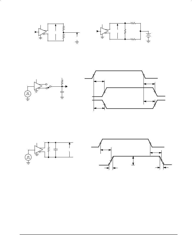
Figure 1. VDD Measurement |
|
Figure 2. Common Mode Test |
|
||
|
VCC |
|
VCC |
375 |
|
|
|
RL/2 |
|
|
|
||
V |
Vin |
VOD3 |
58 |
|
||
VOD2,A |
+ |
|||||
in |
(0.8 or 2.0 V) |
|
||||
(0.8 or 2.0 V) |
RL/2 VOS |
|
|
375 |
VCM = 12 to ±7.0 V |
|
|
|
|
|
|||
Figure 3. Propagation Delay, Single±Ended Outputs
|
|
|
|
3.0 V |
|
VCC |
2.3 V |
Vin |
1.5 V |
1.5 V |
0 V |
tPLH |
|
||||
|
27 Ω |
|
tPHL |
|
|
Y |
|
|
|
||
Vin |
Output |
|
|
|
|
|
|
|
|
|
|
Z |
15 pF |
Output Y |
3.0 V |
3.0 V |
|
S.G. |
|
|
|
|
VOL |
|
|
|
tPLH |
VOH |
|
|
|
|
|
||
|
|
Output Z |
3.0 V |
3.0 V |
|
|
|
|
|
||
|
|
|
tPHL |
|
|
Figure 4. Propagation Delay, Differential Outputs
VCC |
|
|
|
|
|
3.0 V |
|
|
|
1.5 V |
|
1.5 V |
|
|
|
|
Vin |
|
||
|
|
|
|
|
0 V |
|
Vin |
|
50 pF |
V |
tPLHD |
|
|
54 |
|
tPHLD |
||||
|
|
OD |
|
|
||
|
|
|
|
1.5 V |
|
1.5 V |
S.G. |
|
|
VOD |
50% |
[4.6 V |
50% |
|
|
|
|
± 1.5 V |
|
± 1.5 V |
|
|
|
|
tdr |
|
tdf |
NOTES: 1. S.G. set to: f p 1.0 MHz; duty cycle = 50%; tr, tf, p 5.0 ns.
2.tSK1 = tPLHD ± tPHLD for each driver.
3.tSK2 computed by subtracting the shortest tPLHD from the longest tPLHD of the 4 drivers within a package.
4.tSK3 computed by subtracting the shortest tPHLD from the longest tPHLD of the 4 drivers within a package.
4 |
MOTOROLA ANALOG IC DEVICE DATA |
 Loading...