


Texas Instruments JM38510-37701BEA, JM38510-37701B2A, SN54ALS138AJ, SN54AS138J, SN74ALS138AD Datasheet
...SN54ALS138A, SN54AS138, SN74ALS138A, SN74AS138 3-LINE TO 8-LINE DECODERS/DEMULTIPLEXERS
|
|
SDAS055E ± APRIL 1982 ± REVISED JULY 1996 |
||||||
|
|
|
|
|
|
|
|
|
D Designed Specifically for High-Speed |
SN54ALS138A, SN54AS138 . . . J PACKAGE |
|||||||
Memory Decoders and Data Transmission |
SN74ALS138A, SN74AS138 . . . D OR N PACKAGE |
|||||||
Systems |
|
|
|
(TOP VIEW) |
|
|
||
|
|
|
|
|
|
|
|
|
D Incorporate Three Enable Inputs to Simplify |
|
A |
|
|
|
|
VCC |
|
|
|
1 |
16 |
|
||||
|
|
|
||||||
Cascading and/or Data Reception |
|
|
|
|||||
|
B |
|
2 |
15 |
|
Y0 |
||
D Package Options Include Plastic |
|
|
|
|||||
|
C |
|
|
3 |
14 |
|
Y1 |
|
Small-Outline (D) Packages, Ceramic Chip |
|
|
|
|||||
G2A |
|
4 |
13 |
|
Y2 |
|||
Carriers (FK), and Standard Plastic (N) and |
|
|
||||||
|
G2B |
|
|
5 |
12 |
|
Y3 |
|
Ceramic (J) 300-mil DIPs |
|
|
|
|||||
|
G1 |
6 |
11 |
|
Y4 |
|||
|
|
|
||||||
|
|
|
|
|
|
|
|
|
description |
|
|
|
|
|
|
|
Y7 |
7 |
|
10 |
Y5 |
|
|
|
|
|
|
|
|
GND |
8 |
|
9 |
Y6 |
|
|||
|
|
|
|
|
|
|
|
|
||||||
The ′ALS138A and ′AS138 are 3-line to 8-line |
|
|
|
|
|
|
|
|||||||
decoders/demultiplexers |
designed |
for |
high- |
SN54ALS138A, SN54AS138 . . . FK PACKAGE |
||||||||||
performance memory-decoding or data-routing |
||||||||||||||
|
(TOP VIEW) |
|
|
|||||||||||
applications requiring very short propagation |
|
|
|
|
CC |
|
|
|||||||
delay times. In high-performance systems, these |
|
B A |
NC |
Y0 |
|
|||||||||
devices can be used to minimize the effects of |
|
V |
|
|||||||||||
|
|
|
|
|
|
|
||||||||
system |
decoding. |
When |
employed |
with |
C |
3 |
2 |
1 |
20 19 |
Y1 |
||||
high-speed memories with a fast enable circuit, |
4 |
|
|
|
18 |
|||||||||
the delay times of the decoder and the enable time |
G2A |
5 |
|
|
|
17 |
Y2 |
|||||||
of the memory are usually less than the typical |
NC |
6 |
|
|
|
16 |
NC |
|||||||
access time of the memory. The effective system |
G2B |
7 |
|
|
|
15 |
Y3 |
|||||||
delay introduced by the Schottky-clamped system |
G1 |
8 |
|
|
|
14 |
Y4 |
|||||||
decoder is negligible. |
|
|
|
|
|
|
9 |
10 11 12 13 |
|
|||||
|
|
|
|
|
|
|
|
|
|
|
|
|||
The conditions at the binary-select (A, B, and C) |
|
Y7 |
GND |
NC |
Y6 |
Y5 |
|
|||||||
inputs and the three enable (G1, G2A, and G2B) |
|
|
||||||||||||
|
|
|
|
|
|
|
||||||||
inputs select one of eight output lines. Two |
NC ± No internal connection |
|
||||||||||||
active-low and one active-high enable inputs |
|
|
|
|
|
|
|
|||||||
reduce the need for external gates or inverters when expanding. A 24-line decoder can be implemented without |
||||||||||||||
external inverters and a 32-line decoder requires only one inverter. An enable input can be used as a data input |
||||||||||||||
for demultiplexing applications. |
|
|
|
|
|
|
|
|
|
|
||||
The SN54ALS138A and SN54AS138 are characterized for operation over the full military temperature range of ±55°C to 125°C. The SN74ALS138A and SN74AS138 are characterized for operation from 0°C to 70°C.
Please be aware that an important notice concerning availability, standard warranty, and use in critical applications of
Texas Instruments semiconductor products and disclaimers thereto appears at the end of this data sheet.
PRODUCTION DATA information is current as of publication date. Products conform to specifications per the terms of Texas Instruments standard warranty. Production processing does not necessarily include testing of all parameters.
Copyright 1996, Texas Instruments Incorporated
POST OFFICE BOX 655303 •DALLAS, TEXAS 75265 |
1 |
SN54ALS138A, SN54AS138, SN74ALS138A, SN74AS138 3-LINE TO 8-LINE DECODERS/DEMULTIPLEXERS
SDAS055E ± APRIL 1982 ± REVISED JULY 1996
FUNCTION TABLE
|
|
|
|
INPUTS |
|
|
|
|
|
OUTPUTS |
|
|
|
|||
|
|
|
|
|
|
|
|
|
|
|
|
|
|
|
||
|
ENABLE |
|
|
|
SELECT |
|
|
|
|
|
|
|
||||
|
|
|
|
|
|
|
|
|
|
|
|
|
||||
|
|
|
|
|
|
|
|
|
|
|
|
|
|
|
|
|
G1 |
|
|
|
|
|
C |
B |
A |
Y0 |
Y1 |
Y2 |
Y3 |
Y4 |
Y5 |
Y6 |
Y7 |
|
G2A |
|
G2B |
|
||||||||||||
|
|
|
|
|
|
|
|
|
|
|
|
|
|
|
||
X |
|
H |
X |
X |
X |
X |
H |
H |
H |
H |
H |
H |
H |
H |
||
X |
|
X |
H |
X |
X |
X |
H |
H |
H |
H |
H |
H |
H |
H |
||
L |
|
X |
X |
X |
X |
X |
H |
H |
H |
H |
H |
H |
H |
H |
||
H |
|
L |
L |
L |
L |
L |
L |
H |
H |
H |
H |
H |
H |
H |
||
H |
|
L |
L |
L |
L |
H |
H |
L |
H |
H |
H |
H |
H |
H |
||
H |
|
L |
L |
L |
H |
L |
H |
H |
L |
H |
H |
H |
H |
H |
||
H |
|
L |
L |
L |
H |
H |
H |
H |
H |
L |
H |
H |
H |
H |
||
H |
|
L |
L |
H |
L |
L |
H |
H |
H |
H |
L |
H |
H |
H |
||
H |
|
L |
L |
H |
L |
H |
H |
H |
H |
H |
H |
L |
H |
H |
||
H |
|
L |
L |
H |
H |
L |
H |
H |
H |
H |
H |
H |
L |
H |
||
H |
|
L |
L |
H |
H |
H |
H |
H |
H |
H |
H |
H |
H |
L |
||
|
|
|
|
|
|
|
|
|
|
|
|
|
|
|
|
|
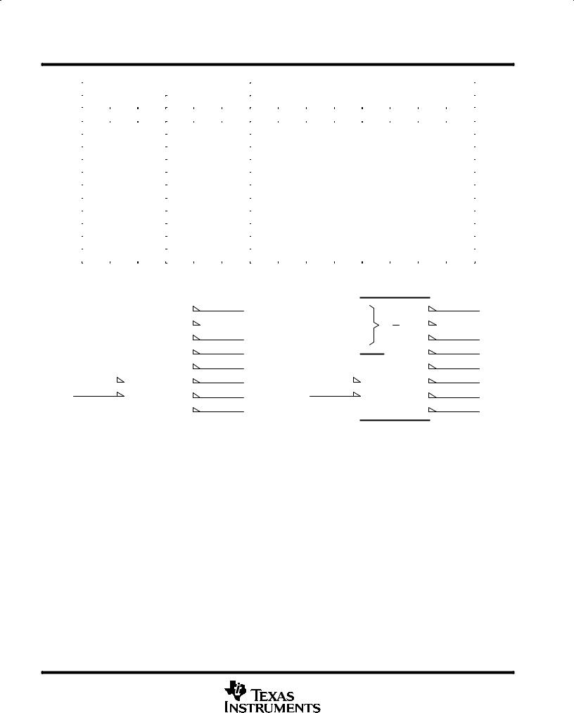
logic symbols (alternatives)²
1 |
|
BIN/OCT |
0 |
15 |
Y0 |
1 |
|
||||||||
A |
|
|
1 |
|
14 |
|
A |
|
|
||||||
|
|
|
|
|
|||||||||||
2 |
|
|
|
|
|
2 |
|
||||||||
B |
|
|
2 |
|
1 |
|
Y1 |
|
B |
|
|
||||
|
|
|
|
|
|
||||||||||
3 |
|
|
|
|
13 |
|
3 |
|
|||||||
C |
|
|
4 |
|
2 |
12 |
Y2 |
|
C |
|
|
||||
|
|
|
|
|
|||||||||||
|
|
|
|
|
|
|
3 |
Y3 |
|
|
|
|
|
|
|
|
|
|
|
|
|
|
|
|
|
|
|
|
|
||
6 |
|
& |
|
11 |
6 |
|
|||||||||
|
|
|
|
|
|||||||||||
G1 |
|
|
|
|
4 |
|
Y4 |
|
G1 |
|
|
||||
|
|
|
|
||||||||||||
|
4 |
|
|
EN |
|
10 |
|
|
|
4 |
|
||||
|
|
|
|
|
|
|
|||||||||
G2A |
|
|
|
5 |
|
Y5 |
G2A |
|
|
||||||
|
|
|
|||||||||||||
|
5 |
|
|
|
6 |
9 |
Y6 |
|
|
5 |
|
||||
G2B |
|
|
7 |
G2B |
|||||||||||
|
|
|
|
|
|
|
7 |
Y7 |
|
|
|
|
|
|
|
|
|
|
|
|
|
|
|
|
|
|
|
|
|
||
|
|
|
|
|
|
|
|
|
|
|
|
|
|
|
|
² These symbols are in accordance with ANSI/IEEE Std 91-1984 and IEC Publication 617-12.
Pin numbers shown are for the D, J, and N packages.
0 |
DMUX |
0 |
15 |
Y0 |
|
|
0 |
14 |
|||
|
G |
1 |
Y1 |
||
2 |
7 |
13 |
|||
|
|
2 |
Y2 |
||
|
|
12 |
|||
|
|
|
3 |
Y3 |
|
& |
|
|
11 |
||
|
|
||||
|
|
|
|
||
|
|
|
4 |
Y4 |
|
|
|
|
10 |
||
|
|
|
5 |
Y5 |
|
|
|
|
9 |
||
|
|
|
6 |
Y6 |
|
|
|
|
7 |
||
|
|
|
7 |
Y7 |
|
|
|
|
|
||
|
|
|
|
|
|
2 |
POST OFFICE BOX 655303 •DALLAS, TEXAS 75265 |

SN54ALS138A, SN54AS138, SN74ALS138A, SN74AS138 3-LINE TO 8-LINE DECODERS/DEMULTIPLEXERS
SDAS055E ± APRIL 1982 ± REVISED JULY 1996
logic diagram (positive logic)
|
|
15 |
|
|
|
Y0 |
|
|
1 |
|
|
|
A |
14 |
|
|
|
||
|
|
Y1 |
|
|
|
13 |
|
Select |
|
Y2 |
|
2 |
|
||
Inputs |
|
||
B |
|
||
|
|
12 |
|
|
|
Y3 |
|
|
|
Data |
|
|
|
Outputs |
|
|
3 |
11 |
|
|
Y4 |
||
|
C |
|
|
|
|
10 |
|
|
|
Y5 |
|
|
|
9 |
|
|
|
Y6 |
|
|
4 |
|
|
|
G2A |
7 |
|
Enable |
5 |
||
Y7 |
|||
Inputs |
G2B |
|
|
|
6 |
|
|
|
G1 |
|
Pin numbers shown are for the D, J, and N packages.
POST OFFICE BOX 655303 •DALLAS, TEXAS 75265 |
3 |
 Loading...