


Texas Instruments JM38510-37201BEA, JM38510-37201B2A, JM38510-37202BEA, JM38510-37202B2A, SN54ALS174J Datasheet
...SN54ALS174, SN54ALS175, SN54AS174, SN54AS175B
SN74ALS174, SN74ALS175, SN74AS174, SN74AS175B
HEX/QUADRUPLE D-TYPE FLIP-FLOPS WITH CLEAR
|
SDAS207D - APRIL 1982 - REVISED MAY 1996 |
|
|
|
|
D 'ALS174 and 'AS174 Contain Six Flip-Flops |
D Fully Buffered Outputs for Maximum |
|
With Single-Rail Outputs |
Isolation From External Disturbances |
|
D 'ALS175 and 'AS175B Contain Four |
('AS Only) |
|
|
||
Flip-Flops With Double-Rail Outputs |
D Package Options Include Plastic |
|
D Buffered Clock and Direct-Clear Inputs |
Small-Outline (D) Packages, Ceramic Chip |
|
Carriers (FK), and Standard Plastic (N) and |
||
D Applications Include: |
||
Ceramic (J) 300-mil DIPs |
||
± Buffer/Storage Registers |
||
|
||
± Shift Registers |
|
|
± Pattern Generators |
|
SN54ALS174, SN54AS174 . . . J PACKAGE SN74ALS174, SN74AS174 . . . D OR N PACKAGE
|
|
|
(TOP VIEW) |
|
|
||
|
|
|
|
|
|
|
VCC |
|
|
|
|
|
|
|
|
|
CLR |
|
|
1 |
16 |
|
|
|
|
||||||
|
1Q |
|
2 |
15 |
|
6Q |
|
|
1D |
|
3 |
14 |
|
6D |
|
|
|
|
|||||
|
2D |
|
4 |
13 |
|
5D |
|
|
|
|
|||||
|
2Q |
|
5 |
12 |
|
5Q |
|
|
|
|
|||||
|
3D |
|
6 |
11 |
|
4D |
|
|
|
|
|||||
|
3Q |
|
7 |
10 |
|
4Q |
|
|
|
|
|||||
GND |
|
8 |
9 |
|
CLK |
||
|
|
||||||
|
|
|
|
|
|
|
|
SN54ALS174, SN54AS174 . . . FK PACKAGE
(TOP VIEW)
|
1Q |
CLR |
NC |
CC |
6Q |
|
|
V |
|
||||
1D |
3 |
2 |
1 |
20 19 |
6D |
|
4 |
|
|
|
18 |
||
2D |
5 |
|
|
|
17 |
5D |
NC |
6 |
|
|
|
16 |
NC |
2Q |
7 |
|
|
|
15 |
5Q |
3D |
8 |
|
|
|
14 |
4D |
|
9 |
10 11 12 13 |
|
|||
|
3Q |
GND |
NC |
CLK |
4Q |
|
NC ± No internal connection
description
SN54ALS175, SN54AS175B . . . J PACKAGE SN74ALS175, SN74AS175B . . . D OR N PACKAGE
|
|
|
|
(TOP VIEW) |
|
|
|
|
||
|
|
|
|
|
|
|
|
VCC |
||
|
|
|
|
|
|
|
|
|||
|
CLR |
|
|
1 |
16 |
|
||||
|
|
|||||||||
|
1Q |
|
2 |
15 |
|
4Q |
||||
|
|
|
|
|
|
|
|
|
|
|
|
1Q |
|
|
3 |
14 |
|
4Q |
|||
|
1D |
|
4 |
13 |
|
4D |
||||
|
|
|
||||||||
|
2D |
|
5 |
12 |
|
3D |
||||
|
|
|
||||||||
|
|
|
|
|
|
|
|
|
|
|
|
2Q |
|
|
6 |
11 |
|
3Q |
|||
|
2Q |
|
7 |
10 |
|
3Q |
||||
|
|
|
||||||||
GND |
|
8 |
9 |
|
CLK |
|||||
|
|
|||||||||
|
|
|
|
|
|
|
|
|
|
|
SN54ALS175A, SN54AS175B . . . FK PACKAGE
|
(TOP VIEW) |
|
||||
|
1Q |
CLR |
NC |
V |
4Q |
|
|
|
|
|
CC |
|
|
1Q |
3 |
2 |
1 |
20 19 |
4Q |
|
4 |
|
|
|
18 |
||
1D |
5 |
|
|
|
17 |
4D |
NC |
6 |
|
|
|
16 |
NC |
2D |
7 |
|
|
|
15 |
3D |
2Q |
8 |
|
|
|
14 |
3Q |
|
9 |
10 11 12 13 |
|
|||
|
2Q |
GND |
NC |
CLK |
3Q |
|
These positive-edge-triggered flip-flops utilize TTL circuitry to implement D-type flip-flop logic. All have a direct-clear (CLR) input. The 'ALS175 and 'AS175B feature complementary outputs from each flip-flop.
Information at the data (D) inputs meeting the setup-time requirements is transferred to the outputs on the positive-going edge of the clock pulse. Clock triggering occurs at a particular voltage level and is not directly related to the transition time of the positive-going pulse. When the clock (CLK) input is at either the high or low level, the D-input signal has no effect at the output.
Please be aware that an important notice concerning availability, standard warranty, and use in critical applications of Texas Instruments semiconductor products and disclaimers thereto appears at the end of this data sheet.
PRODUCTION DATA information is current as of publication date. Products conform to specifications per the terms of Texas Instruments standard warranty. Production processing does not necessarily include testing of all parameters.
Copyright 1996, Texas Instruments Incorporated
POST OFFICE BOX 655303 •DALLAS, TEXAS 75265 |
1 |
SN54ALS174, SN54ALS175, SN54AS174, SN54AS175B
SN74ALS174, SN74ALS175, SN74AS174, SN74AS175B
HEX/QUADRUPLE D-TYPE FLIP-FLOPS WITH CLEAR
SDAS207D - APRIL 1982 - REVISED MAY 1996
description (continued)
These circuits are fully compatible for use with most TTL circuits.
The SN54ALS174, SN54ALS175, SN54AS174, and SN54AS175B are characterized for operation over the full military temperature range of ±55°C to 125°C. The SN74ALS174, SN74ALS175, SN74AS174, and SN74AS175B are characterized for operation from 0°C to 70°C.
FUNCTION TABLE (each flip-flop)
|
|
INPUTS |
|
OUTPUTS |
|||
|
|
|
|
|
|
|
|
|
|
CLK |
D |
Q |
|
|
² |
|
CLR |
Q |
|||||
|
|
|
|
|
|
|
|
|
L |
X |
X |
L |
H |
||
|
H |
↑ |
H |
H |
L |
||
|
H |
↑ |
L |
L |
H |
||
|
H |
L |
X |
Q0 |
|
||
|
Q |
0 |
|||||
² 'ALS175 and 'AS175B only |
|
|
|
||||
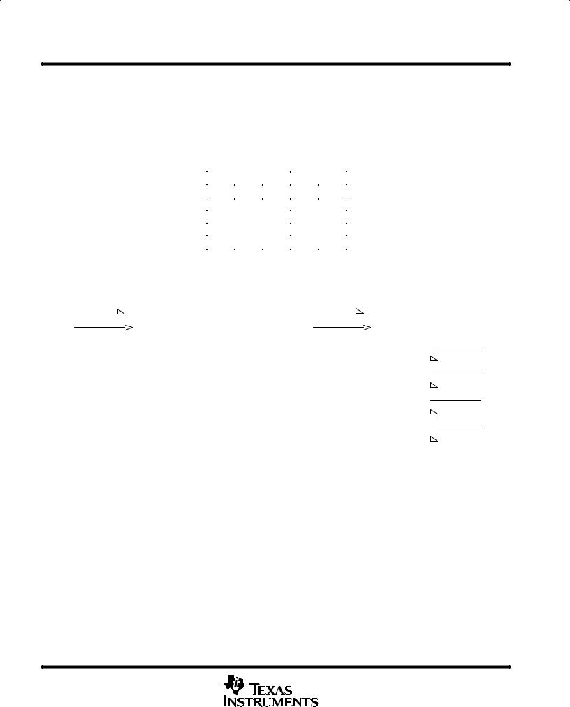
logic symbols³
|
|
|
|
'ALS174, 'AS174 |
|
|
|
|
|
'ALS175, 'AS175B |
|
|
|
|||||
|
|
1 |
|
|
|
|
|
|
|
1 |
|
|
|
|
|
|
||
CLR |
|
R |
|
|
CLR |
|
R |
|
|
|
||||||||
|
|
|
|
|
|
|
||||||||||||
|
|
|
|
|
|
|||||||||||||
9 |
|
C1 |
|
|
9 |
|
C1 |
|
|
|
||||||||
|
CLK |
|
|
|
|
CLK |
|
|
|
|
||||||||
3 |
|
|
|
2 |
|
4 |
|
|
|
2 |
1Q |
|||||||
|
|
|
|
|
|
|
||||||||||||
|
1D |
|
1D |
|
1Q |
|
|
|
3 |
|||||||||
|
|
|
|
|
||||||||||||||
4 |
|
5 |
|
|
1D |
|
1D |
|
|
|||||||||
|
|
|
2Q |
|
|
1Q |
||||||||||||
|
|
|
|
|
|
|
|
|
|
|
|
|
|
|
|
|||
|
2D |
|
|
|
|
|
|
|
|
|
|
|
7 |
|
|
|||
6 |
|
7 |
|
5 |
|
|
|
2Q |
||||||||||
|
|
|
|
|
|
|
||||||||||||
|
3D |
|
|
|
|
|
3Q |
|
|
|
6 |
|||||||
|
|
|
|
|
|
|
|
|||||||||||
11 |
|
10 |
|
|
2D |
|
|
|
|
|
|
|||||||
|
|
|
|
|
|
|
|
|
2Q |
|||||||||
|
4D |
|
|
|
|
|
4Q |
|
|
|
|
|
|
|
|
|||
|
|
|
|
|
|
|
|
|
|
|
|
|
10 |
|||||
|
|
|
|
|
|
|
|
|
|
|
|
|||||||
13 |
|
12 |
|
12 |
|
|
|
3Q |
||||||||||
|
|
|
|
|
|
|
||||||||||||
|
5D |
|
|
|
|
|
5Q |
|
|
|
11 |
|||||||
|
|
|
|
|
|
|
|
|||||||||||
14 |
|
15 |
|
|
3D |
|
|
|
|
|
|
|||||||
|
|
|
6Q |
|
|
|
|
|
3Q |
|||||||||
|
6D |
|
|
|
|
|
|
|
|
|
|
|
|
|
||||
|
|
|
|
|
|
|
|
|
|
|
|
|
15 |
|||||
|
|
|
|
|
|
|
|
|
|
|
|
|||||||
|
|
|
|
|
|
|
|
|
13 |
|
|
|
4Q |
|||||
|
|
|
|
|
|
|
|
|
|
|
|
14 |
||||||
|
|
|
|
|
|
|
|
|
|
4D |
|
|
|
|
|
|
||
|
|
|
|
|
|
|
|
|
|
|
|
|
|
|
|
|||
|
|
|
|
|
|
|
|
|
|
|
|
|
|
4Q |
||||
³ These symbols are in accordance with ANSI/IEEE Std 91-1984 and IEC Publication 617-12. |
|
|
|
|
||||||||||||||
|
|
|
|
|
|
|||||||||||||
|
|
|
|
|
|
|||||||||||||
Pin numbers shown are for the D, J, and N packages. |
|
|
|
|
|
|
|
|
|
|
|
|||||||
2 |
POST OFFICE BOX 655303 •DALLAS, TEXAS 75265 |

|
|
|
SN54ALS174, SN54ALS175, SN54AS174, SN54AS175B |
|||
|
|
|
SN74ALS174, SN74ALS175, SN74AS174, SN74AS175B |
|||
|
|
|
HEX/QUADRUPLE D-TYPE FLIP-FLOPS WITH CLEAR |
|||
|
|
|
|
SDAS207D - APRIL 1982 - REVISED MAY 1996 |
||
logic diagrams (positive logic) |
|
|
|
|||
|
|
'ALS174, 'AS174 |
|
'ALS175, 'AS175B |
|
|
CLR |
1 |
|
CLR |
1 |
|
|
|
|
|
||||
|
|
|
|
|||
CLK |
9 |
|
CLK |
9 |
|
|
|
|
|
||||
|
|
|
|
|||
|
3 |
|
|
4 |
2 |
|
1D |
1D |
1D |
1D |
|||
|
1Q |
|||||
|
|
C1 |
2 |
C1 |
|
|
|
|
1Q |
3 |
|||
|
|
R |
|
R |
||
|
|
|
1Q |
|||
To Five Other Channels |
To Three Other Channels |
Pin numbers shown are for the D, J, and N packages.
absolute maximum ratings over operating free-air temperature range (unless otherwise noted)²
Supply voltage, VCC . . . . . . . . . . . . . . . . . . . . . . . . . . . . . . . . . . . . . . . . . . . . . . . . . . . . . . . . . . . . . . |
. . . . . . . . . 7 V |
Input voltage, VI . . . . . . . . . . . . . . . . . . . . . . . . . . . . . . . . . . . . . . . . . . . . . . . . . . . . . . . . . . . . . . . . . . |
. . . . . . . . . 7 V |
Operating free-air temperature range, TA: SN54ALS174, SN54ALS175 . . . . . . . . . . . . . . . . |
±55°C to 125°C |
SN74ALS174, SN74ALS175 . . . . . . . . . . . . . . . . . . |
. . 0°C to 70°C |
Storage temperature range, Tstg . . . . . . . . . . . . . . . . . . . . . . . . . . . . . . . . . . . . . . . . . . . . . . . . . . |
±65°C to 150°C |
²Stresses beyond those listed under ªabsolute maximum ratingsº may cause permanent damage to the device. These are stress ratings only, and functional operation of the device at these or any other conditions beyond those indicated under ªrecommended operating conditionsº is not implied. Exposure to absolute-maximum-rated conditions for extended periods may affect device reliability.
recommended operating conditions
|
|
|
|
|
SN54ALS174 |
SN74ALS174 |
|
||||
|
|
|
|
|
SN54ALS175 |
SN74ALS175 |
UNIT |
||||
|
|
|
|
|
|
|
|
|
|
|
|
|
|
|
|
|
MIN |
NOM |
MAX |
MIN |
NOM |
MAX |
|
|
|
|
|
|
|
|
|
|
|
|
|
VCC |
Supply voltage |
|
|
|
4.5 |
5 |
5.5 |
4.5 |
5 |
5.5 |
V |
VIH |
High-level input voltage |
|
|
|
2 |
|
|
2 |
|
|
V |
VIL |
Low-level input voltage |
|
|
|
|
|
0.8 |
|
|
0.8 |
V |
IOH |
High-level output current |
|
|
|
|
|
±0.4 |
|
|
±0.4 |
mA |
IOL |
Low-level output current |
|
|
|
|
|
4 |
|
|
8 |
mA |
fclock |
Clock frequency |
|
|
|
0 |
|
40 |
0 |
|
50 |
MHz |
|
|
|
CLR |
low |
15 |
|
|
10 |
|
|
|
tw |
Pulse duration |
|
|
|
|
|
|
|
|
ns |
|
|
CLK high |
12.5 |
|
|
10 |
|
|
||||
|
|
CLK low |
12.5 |
|
|
10 |
|
|
|
||
|
|
|
|
|
|
|
|
|
|
||
tsu |
Setup time before CLK↑ |
Data |
15 |
|
|
10 |
|
|
ns |
||
|
|
|
|
|
|
|
|
|
|||
|
|
|
|
|
|
|
|
|
|||
CLR inactive |
8 |
|
|
6 |
|
|
|||||
|
|
|
|
|
|
|
|||||
|
|
|
|
|
|
|
|
|
|
|
|
th |
Hold time, data after CLK↑ |
|
|
|
0 |
|
|
0 |
|
|
ns |
TA |
Operating free-air temperature |
|
|
|
±55 |
|
125 |
0 |
|
70 |
°C |
POST OFFICE BOX 655303 •DALLAS, TEXAS 75265 |
3 |
 Loading...