


Texas Instruments JM38510-36101B2A, JM38510-36101BFA, JM38510-36101BEA, SN54173J, SN54LS173AJ Datasheet
...
|
|
|
|
|
|
|
|
|
SN54173, SN54LS173A, SN74173, SN74LS173A |
|||||||||||||||||||
|
|
|
|
|
|
|
|
|
|
|
|
|
|
4-BIT D-TYPE REGISTERS |
||||||||||||||
|
|
|
|
|
|
|
|
|
|
|
|
|
|
|
|
WITH 3-STATE OUTPUTS |
||||||||||||
|
|
|
|
|
|
|
|
|
SDLS067A ± OCTOBER 1976 ± REVISED JUNE 1999 |
|||||||||||||||||||
|
|
|
|
|
|
|
|
|
|
|
|
|
|
|
|
|
|
|
|
|
|
|
|
|||||
D 3-State Outputs Interface Directly With |
SN54173, SN54LS173A . . . J OR W PACKAGE |
|||||||||||||||||||||||||||
System Bus |
|
|
|
|
|
|
SN74173 . . . N PACKAGE |
|
|
|||||||||||||||||||
D Gated Output-Control LInes for Enabling or |
SN74LS173A . . . D or N PACKAGE |
|||||||||||||||||||||||||||
|
|
|
|
|
(TOP VIEW) |
|
|
|
|
|
|
|
||||||||||||||||
Disabling the Outputs |
|
|
|
|
|
|
M |
|
|
|
|
|
|
|
|
|
VCC |
|
|
|||||||||
|
|
|
|
|
|
|
1 |
|
|
|
16 |
|
|
|
|
|||||||||||||
D Fully Independent Clock Virtually |
|
|
|
|
|
|
|
|
|
|
|
|
|
|||||||||||||||
|
|
|
|
|
|
|
|
|
|
|
|
|
||||||||||||||||
|
|
|
|
|
|
|
|
|
|
|
|
|
|
|||||||||||||||
Eliminates Restrictions for Operating in |
|
|
|
N |
|
2 |
|
|
|
15 |
|
|
CLR |
|
|
|||||||||||||
|
|
|
|
|
|
|
|
|
|
|
|
|||||||||||||||||
One of Two Modes: |
|
|
|
|
|
1Q |
|
3 |
|
|
|
14 |
|
|
1D |
|
|
|||||||||||
|
|
|
|
|
|
|
|
|
|
|
|
|
|
|
||||||||||||||
± |
Parallel Load |
|
|
|
|
|
2Q |
|
4 |
|
|
|
13 |
|
|
2D |
|
|
||||||||||
± Do Nothing (Hold) |
|
|
|
|
|
3Q |
|
5 |
|
|
|
12 |
|
|
3D |
|
|
|||||||||||
|
|
|
|
|
|
|
|
|
|
|
|
|
||||||||||||||||
D For Application as Bus Buffer Registers |
|
|
4Q |
|
6 |
|
|
|
11 |
|
|
4D |
|
|
||||||||||||||
|
|
|
|
|
|
|
|
|
|
|||||||||||||||||||
|
|
|
7 |
|
|
|
10 |
|
|
|
|
|||||||||||||||||
|
|
|
|
|
|
|
|
|
|
CLK |
|
|
|
|
|
|
|
|
|
|
|
|
||||||
D Package Options Include Plastic |
|
|
|
|
|
|
|
G2 |
|
|
||||||||||||||||||
|
|
|
|
|
|
|
|
8 |
|
|
|
9 |
|
|
|
|
|
|
|
|
||||||||
|
|
GND |
|
|
|
|
|
|
G1 |
|
|
|||||||||||||||||
Small-Outline (D) Packages, Ceramic Flat |
|
|
|
|
|
|
|
|
||||||||||||||||||||
|
|
|
|
|
|
|
|
|
|
|
|
|
|
|
|
|
|
|
|
|||||||||
(W) Packages, Ceramic Chip Carriers (FK), |
|
|
|
|
|
|
|
|
|
|
|
|
|
|
|
|
|
|
|
|
||||||||
and Standard Plastic (N) and Ceramic (J) |
SN54LS173A . . . FK PACKAGE |
|||||||||||||||||||||||||||
DIPs |
|
|
|
|
|
|
|
|
|
|
|
(TOP VIEW) |
|
|
|
|
|
|
|
|||||||||
|
|
|
|
|
|
|
|
|
|
|
|
|
|
|
|
|
|
|
|
CC |
CLR |
|
|
|||||
|
|
|
|
TYPICAL |
|
MAXIMUM |
|
|
|
|
|
|
|
|
|
|
|
|
|
|
||||||||
|
|
|
|
|
|
|
|
|
|
N |
|
M |
NC V |
|
|
|||||||||||||
|
TYPE |
|
PROPAGATION |
|
CLOCK |
|
|
|
|
|
|
|
|
|||||||||||||||
|
|
|
DELAY TIME |
|
FREQUENCY |
|
|
|
|
|
|
|
|
|
|
|
|
|
|
|
|
|
|
|
|
|
||
|
|
|
|
|
1Q |
|
|
3 |
2 |
|
1 |
|
20 19 |
|
|
|
|
1D |
||||||||||
|
|
|
|
|
|
|
|
|
|
|
|
|
|
|
|
|
||||||||||||
|
'173 |
|
|
23 ns |
|
35 MHz |
|
|
|
4 |
|
|
|
|
|
|
|
|
|
18 |
|
|
||||||
|
'LS173A |
|
|
18 ns |
|
50 MHz |
|
2Q |
|
|
5 |
|
|
|
|
|
|
|
|
|
17 |
|
|
2D |
||||
|
|
|
|
|
NC |
|
|
|
|
|
|
|
|
|
|
|
|
16 |
|
|
NC |
|||||||
|
|
|
|
|
|
|
|
|
|
|
6 |
|
|
|
|
|
|
|
|
|
|
|
||||||
description |
|
|
|
|
|
|
|
|
|
|
|
|
|
|||||||||||||||
|
|
|
|
|
|
3Q |
|
|
|
|
|
|
|
|
|
|
|
|
15 |
|
|
3D |
||||||
|
|
|
|
|
|
|
|
7 |
|
|
|
|
|
|
|
|
|
|
|
|||||||||
The '173 and 'LS173A 4-bit registers include |
4Q |
|
|
8 |
|
|
|
|
|
|
|
|
|
14 |
|
|
4D |
|||||||||||
|
|
|
9 10 11 12 13 |
|
|
|
|
|
|
|||||||||||||||||||
D-type flip-flops featuring totem-pole 3-state |
|
|
|
|
|
|
|
|
|
|
|
|
|
|
|
|
|
|
|
|
||||||||
|
|
|
|
|
|
|
|
|
|
|
|
|
|
|
|
|
|
|
|
|||||||||
outputs capable |
of driving |
highly |
capacitive |
|
|
|
|
|
|
|
|
|
|
|
|
|
|
|
|
|
|
|
|
|||||
|
|
|
|
|
|
|
|
|
|
|
|
|
|
|
|
|
|
|
|
|||||||||
|
|
|
|
CLK |
|
GND |
NC |
G1 |
G2 |
|
|
|||||||||||||||||
or |
relatively |
|
low-impedance loads. The |
|
|
|
|
|
|
|
||||||||||||||||||
|
NC ± No internal connection |
|
|
|||||||||||||||||||||||||
high-impedance |
third state |
and |
increased |
|
|
|||||||||||||||||||||||
|
|
|
|
|
|
|
|
|
|
|
|
|
|
|
|
|
|
|
|
|||||||||
high-logic-level drive provide these flip-flops with the capability of being connected directly to and
driving the bus lines in a bus-organized system without need for interface or pull-up components. Up to 128 of the SN74173 or SN74LS173A outputs can be connected to a common bus and still drive two Series 54/74 or 54LS/74LS TTL normalized loads, respectively. Similarly, up to 49 of the SN54173 or SN54LS173A outputs can be connected to a common bus and drive one additional Series 54/74 or 54LS/74LS TTL normalized load, respectively. To minimize the possibility that two outputs will attempt to take a common bus to opposite logic levels, the output control circuitry is designed so that the average output disable times are shorter than the average output enable times.
Gated enable inputs are provided on these devices for controlling the entry of data into the flip-flops. When both data-enable (G1, G2) inputs are low, data at the D inputs are loaded into their respective flip-flops on the next positive transition of the buffered clock input. Gate output-control (M, N) inputs also are provided. When both are low, the normal logic states (high or low levels) of the four outputs are available for driving the loads or bus lines. The outputs are disabled independently from the level of the clock by a high logic level at either output-control input. The outputs then present a high impedance and neither load nor drive the bus line. Detailed operation is given in the function table.
The SN54173 and SN54LS173A are characterized for operation over the full military temperature range of ±55°C to 125°C. The SN74173 and SN74LS173A are characterized for operation from 0°C to 70°C.
Please be aware that an important notice concerning availability, standard warranty, and use in critical applications of
Texas Instruments semiconductor products and disclaimers thereto appears at the end of this data sheet.
PRODUCTION DATA information is current as of publication date. Products conform to specifications per the terms of Texas Instruments standard warranty. Production processing does not necessarily include testing of all parameters.
Copyright 1999, Texas Instruments Incorporated
On products compliant to MIL-PRF-38535, all parameters are tested unless otherwise noted. On all other products, production processing does not necessarily include testing of all parameters.
POST OFFICE BOX 655303 •DALLAS, TEXAS 75265 |
1 |
SN54173, SN54LS173A, SN74173, SN74LS173A 4-BIT D-TYPE REGISTERS
WITH 3-STATE OUTPUTS
SDLS067A ± OCTOBER 1976 ± REVISED JUNE 1999
FUNCTION TABLE
|
|
INPUTS |
|
|
|
OUTPUT |
|||
|
|
|
|
|
|
|
|
||
|
|
DATA ENABLE |
DATA |
||||||
CLR |
CLK |
Q |
|||||||
|
|
|
|
|
D |
||||
G1 |
G2 |
||||||||
|
|
|
|||||||
H |
X |
|
X |
X |
X |
L |
|||
L |
L |
|
X |
X |
X |
Q0 |
|||
L |
↑ |
|
H |
X |
X |
Q0 |
|||
L |
↑ |
|
X |
H |
X |
Q0 |
|||
L |
↑ |
|
L |
L |
L |
L |
|||
L |
↑ |
|
L |
L |
H |
H |
|||
|
|
|
|
|
|
|
|
|
|
When either M or N (or both) is (are) high, the output is disabled to the high-impedance state; however, sequential operation of the flip-flops is not affected.
logic symbol²
|
|
|
|
|
|
|
'173 |
|
|
|
|
|
|
|
|
|
|
|
|
'LS173A |
||||||
15 |
|
|
|
|
|
|
15 |
|
|
|
|
|
|
|
||||||||||||
CLR |
|
R |
|
|
CLR |
|
R |
|
|
|
|
|
||||||||||||||
|
|
|
|
|
|
|
|
|
||||||||||||||||||
1 |
|
|
|
|
|
|
1 |
|
|
|
|
|
|
|
||||||||||||
& |
|
|
|
|
& |
|
|
|
|
|
||||||||||||||||
|
|
M |
|
|
|
|
|
|
|
M |
|
|
|
|
|
|
||||||||||
|
|
|
|
|
|
|
|
|
|
|
|
|
|
|
|
|
|
|
||||||||
2 |
|
|
EN |
|
|
2 |
|
|
|
EN |
|
|||||||||||||||
|
|
N |
|
|
|
|
|
|
|
|
|
N |
|
|
|
|
|
|
|
|
||||||
|
|
|
|
|
|
|
|
|
|
|
|
|
|
|
|
|
|
|
||||||||
|
|
9 |
|
|
|
|
|
|
|
|
9 |
|
|
|
|
|
|
|
||||||||
|
|
|
& |
|
|
|
|
|
|
|
& |
|
|
|
|
|
||||||||||
|
|
G1 |
|
|
|
|
|
|
|
G1 |
|
|
|
|
|
|
||||||||||
|
|
|
|
|
|
|
|
|
|
|
|
|
|
|
||||||||||||
|
|
|
10 |
|
|
C1 |
|
|
|
|
|
10 |
|
|
|
C1 |
|
|
||||||||
|
G2 |
|
|
|
|
|
G2 |
|
|
|
|
|
||||||||||||||
|
|
|
|
|
|
|
|
|
||||||||||||||||||
7 |
|
|
|
|
|
|
7 |
|
|
|
|
|
|
|
||||||||||||
CLK |
|
|
|
|
|
|
|
CLK |
|
|
|
|
|
|
|
|
||||||||||
|
|
|
|
|
|
|
|
|
|
|
|
|
|
|
||||||||||||
14 |
|
|
|
|
3 |
|
14 |
|
|
|
|
|
3 |
|
||||||||||||
|
|
|
|
|
|
|
|
|
|
|
||||||||||||||||
1D |
1D |
|
1Q |
|
|
1D |
1D |
|
|
|
|
1Q |
||||||||||||||
4 |
|
|
4 |
|||||||||||||||||||||||
13 |
|
|
|
|
2Q |
13 |
|
|
|
|
2Q |
|||||||||||||||
|
|
|
|
|
|
|
|
|||||||||||||||||||
2D |
|
|
|
|
|
|
|
|
2D |
|
|
|
|
|
|
|
||||||||||
|
|
|
|
|
|
|
|
|
|
|
|
|||||||||||||||
12 |
|
|
|
|
5 |
|
12 |
|
|
|
|
5 |
|
|||||||||||||
|
|
|
|
|
|
|
|
|
||||||||||||||||||
3D |
|
|
|
|
|
|
3Q |
|
|
3D |
|
|
|
|
|
|
|
3Q |
||||||||
|
|
|
|
|
|
|
|
|
|
|
|
|||||||||||||||
11 |
|
|
|
|
6 |
|
11 |
|
|
|
|
6 |
|
|||||||||||||
|
|
|
|
|
|
|
|
|
||||||||||||||||||
4D |
|
|
|
|
|
|
4Q |
|
|
4D |
|
|
|
|
|
|
|
4Q |
||||||||
|
|
|
|
|
|
|
|
|
|
|
|
|||||||||||||||
|
|
|
|
|
|
|
|
|
|
|
|
|
|
|
|
|
|
|
|
|
|
|
|
|
|
|
² This symbol is in accordance with ANSI/IEEE Standard 91-1984 and IEC Publication 617-12.
Pin numbers shown are for D, J, N, and W packages.
2 |
POST OFFICE BOX 655303 •DALLAS, TEXAS 75265 |

|
|
SN54173, SN54LS173A, SN74173, SN74LS173A |
|
|
|
|
4-BIT D-TYPE REGISTERS |
|
|
|
WITH 3-STATE OUTPUTS |
|
|
SDLS067A ± OCTOBER 1976 ± REVISED JUNE 1999 |
|
logic diagram (positive logic) |
|
|
|
|
1 |
|
|
Output |
M |
|
|
|
|
|
|
Control |
2 |
|
|
|
N |
|
|
|
14 |
1D |
|
|
|
|
|
|
1D |
|
|
|
9 |
C1 |
|
|
|
|
|
Data |
G1 |
|
3 |
|
R |
||
Enable |
10 |
1Q |
|
|
|
||
|
G2 |
|
|
|
13 |
1D |
|
|
|
|
|
|
2D |
|
|
|
|
C1 |
|
|
|
R |
4 |
|
7 |
2Q |
|
|
CLK |
|
|
|
12 |
1D |
|
|
|
|
|
|
3D |
|
|
|
|
C1 |
|
|
|
R |
5 |
|
|
3Q |
|
|
11 |
1D |
|
|
|
|
|
|
4D |
|
|
|
|
C1 |
|
|
|
R |
6 |
|
15 |
4Q |
|
|
|
|
|
|
CLR |
|
|
Pin numbers shown are for D, J, N, and W packages.
POST OFFICE BOX 655303 •DALLAS, TEXAS 75265 |
3 |
SN54173, SN54LS173A, SN74173, SN74LS173A 4-BIT D-TYPE REGISTERS
WITH 3-STATE OUTPUTS
SDLS067A ± OCTOBER 1976 ± REVISED JUNE 1999
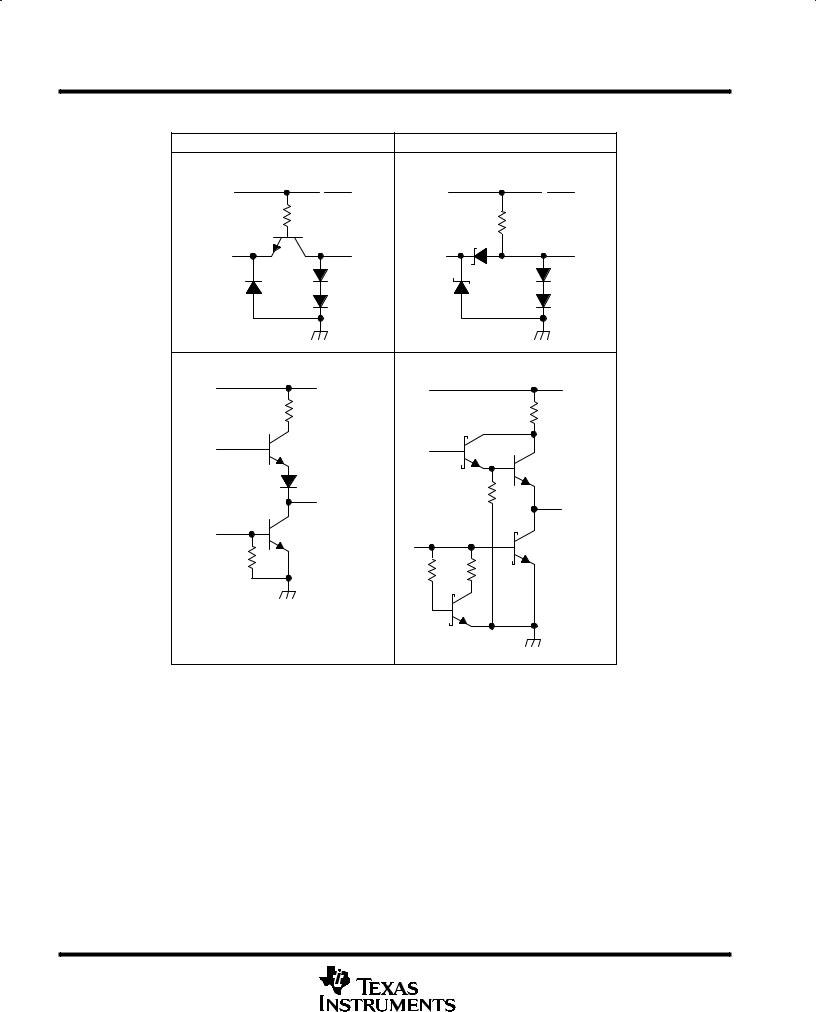
schematics of inputs and outputs
'173 |
'LS173A |
Equivalent of Each Input |
Equivalent of Each Input |
VCC |
VCC |
4 kΩ NOM |
20 kΩ NOM |
|
|
Input |
Input |
Typical of All Outputs |
Typical of All Outputs |
VCC |
V |
|
CC |
90 Ω NOM |
100 Ω NOM |
Output
Output
absolute maximum ratings over operating free-air temperature range (unless otherwise noted)²
Supply voltage, VCC (see Note 1) . . . . . . . . . . . . . . . . . . . . . . . . . . . . . . . . . . . . . . . . . . . . . . . . . . . |
. ±0.5 V to 7 |
V |
Input voltage: '173 . . . . . . . . . . . . . . . . . . . . . . . . . . . . . . . . . . . . . . . . . . . . . . . . . . . . . . . . . . . . . . . . |
±0.5 V to 5.5 |
V |
'LS173A . . . . . . . . . . . . . . . . . . . . . . . . . . . . . . . . . . . . . . . . . . . . . . . . . . . . . . . . . . . . |
. ±0.5 V to 7 V |
|
Off-state output voltage . . . . . . . . . . . . . . . . . . . . . . . . . . . . . . . . . . . . . . . . . . . . . . . . . . . . . . . . . . . . |
±0.5 V to 5.5 |
V |
Package thermal impedance, θJA (see Note 2): D package . . . . . . . . . . . . . . . . . . . . . . . . . . . . . |
. . . . . 113°C/W |
|
N package . . . . . . . . . . . . . . . . . . . . . . . . . . . . . |
. . . . . . 78°C/W |
|
Storage temperature range, Tstg . . . . . . . . . . . . . . . . . . . . . . . . . . . . . . . . . . . . . . . . . . . . . . . . . . . |
±65°C to 150°C |
|
² Stresses beyond those listed under ªabsolute maximum ratingsº may cause permanent damage to the device. These are stress ratings only, and functional operation of the device at these or any other conditions beyond those indicated under ªrecommended operating conditionsº is not implied. Exposure to absolute-maximum-rated conditions for extended periods may affect device reliability.
NOTES: 1. Voltage values are with respect to network ground terminal.
2.The package thermal impedance is calculated in accordance with JESD 51, except for through-hole packages, which use a trace length of zero.
4 |
POST OFFICE BOX 655303 •DALLAS, TEXAS 75265 |
 Loading...