


Texas Instruments JM38510-34102BEA, JM38510-34102B2A, JM38510-34102BFA, SN74F109D, SN74F109DR Datasheet
...
SN54F109, SN74F109 DUAL J-K POSITIVE-EDGE-TRIGGERED FLIP-FLOPS WITH CLEAR AND PRESET
SDFS047A ± MARCH 1987 ± REVISED OCTOBER 1993
•Package Options Include Plastic Small-Outline Packages, Ceramic Chip Carriers, and Standard Plastic and Ceramic 300-mil DIPs
description
These devices contain two independent J-K positive-edge-triggered flip-flops. A low level at
the preset (PRE) or clear (CLR) inputs sets or resets the outputs regardless of the levels of the
other inputs. When PRE and CLR are inactive
(high), data at the J and K input meeting the setup-time requirements are transferred to the outputs on the positive-going edge of the clock pulse. Clock triggering occurs at a voltage level and is not directly related to the rise time of the clock pulse. Following the hold time interval, data
at the J and K inputs may be changed without affecting the levels at the outputs. These versatile flip-flops can perform as toggle flip-flops by grounding K and trying J high. They also can perform as D-type flip-flops if J and K are tied together.
The SN54F109 is characterized for operation over the full military temperature range of ±55°C to 125°C. The SN74F109 is characterized for operation from 0°C to 70°C.
SN54F109 . . . J PACKAGE SN74F109 . . . D OR N PACKAGE
|
|
|
|
|
|
(TOP VIEW) |
|
|
|
|
|
|
|
|
|
|
|
|
|
VCC |
|||
|
|
|
|
|
|
|
|
||||
|
1CLR |
|
|
1 |
16 |
||||||
|
|
|
|||||||||
|
1J |
|
|
|
|
|
|
|
|||
|
|
2 |
15 |
|
2CLR |
||||||
|
|
|
|
|
|
|
|
2J |
|||
|
1K |
|
|
3 |
14 |
||||||
1CLK |
|
|
|
|
|
|
|
||||
|
4 |
13 |
2K |
|
|
||||||
|
|
|
|
|
|
|
|
2CLK |
|||
|
1PRE |
|
|
5 |
12 |
||||||
|
1Q |
|
|
|
|
|
|
|
|||
|
|
6 |
11 |
|
2PRE |
||||||
|
|
|
|
|
|
|
|
2Q |
|||
|
1Q |
|
|
7 |
10 |
||||||
GND |
|
|
|
|
|
|
|
||||
|
8 |
9 |
2Q |
|
|||||||
|
|
|
|
|
|
|
|
|
|
|
|
SN54F109 . . . FK PACKAGE |
|||||
|
|
(TOP VIEW) |
|
||
|
1J |
1CLR |
NC |
V 2CLR |
|
|
|
|
|
CC |
|
1K |
3 |
2 |
1 |
20 19 |
2J |
4 |
|
|
18 |
||
1CLK |
5 |
|
|
17 |
2K |
NC |
6 |
|
|
16 |
NC |
1PRE |
7 |
|
|
15 |
2CLK |
1Q |
8 |
|
|
14 |
2PRE |
|
9 |
10 11 12 13 |
|
||
|
1Q |
GND |
NC |
2Q 2Q |
|
NC ± No internal connection |
|
||||
FUNCTION TABLE
|
|
|
|
INPUTS |
|
|
|
OUTPUTS |
|||||
|
|
|
|
|
|
|
|
|
|
|
|
||
|
|
|
|
CLK |
J |
|
|
Q |
|
|
|
|
|
|
PRE |
|
CLR |
K |
|
|
Q |
|
|||||
|
L |
H |
X |
X |
X |
H |
|
L |
|||||
|
H |
L |
X |
X |
X |
L |
|
H |
|||||
|
L |
L |
X |
X |
X |
H² |
H² |
||||||
|
H |
H |
↑ |
L |
L |
L |
|
H |
|||||
|
H |
H |
↑ |
H |
L |
Toggle |
|||||||
|
H |
H |
↑ |
L |
H |
Q0 |
|
|
|||||
|
Q |
0 |
|||||||||||
|
H |
H |
↑ |
H |
H |
H |
|
L |
|||||
|
H |
H |
L |
X |
X |
Q0 |
|
||||||
|
Q |
0 |
|||||||||||
²The output levels are not guaranteed to meet the minimum
levels for VOH. Furthermore, this configuration is nonstable; that is, it will not persist when PRE or CLR returns to its inactive (high) level.
PRODUCTION DATA information is current as of publication date. Products conform to specifications per the terms of Texas Instruments standard warranty. Production processing does not necessarily include testing of all parameters.
Copyright 1993, Texas Instruments Incorporated
POST OFFICE BOX 655303 •DALLAS, TEXAS 75265 |
2±1 |
SN54F109, SN74F109
DUAL J-K POSITIVE-EDGE-TRIGGERED FLIP-FLOPS
WITH CLEAR AND PRESET
SDFS047A ± MARCH 1987 ± REVISED OCTOBER 1993
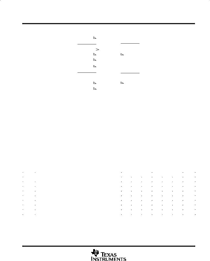
logic symbol²
|
|
|
5 |
S |
|
|
|
||
1PRE |
|
|
6 |
|
|
||||
|
|
|
|
||||||
2 |
1J |
1Q |
|||||||
|
1J |
|
|||||||
4 |
|
|
|
|
|||||
1CLK |
|
|
C1 |
|
|
|
|||
|
|
|
|
|
|||||
|
|
3 |
1K |
7 |
|
|
|||
|
1K |
|
|
|
|
1Q |
|||
1 |
|
||||||||
|
|
|
|
|
|
|
|||
1CLR |
|
|
R |
|
|
|
|||
|
|
|
|
|
|||||
|
|
|
11 |
|
|
|
|
||
|
|
|
|
||||||
|
2PRE |
|
|
|
|
|
|
|
|
|
|
|
|
|
|
||||
14 |
|
10 |
2Q |
||||||
|
2J |
|
|
||||||
12 |
|
|
|
|
|||||
2CLK |
|
|
|
9 |
|
|
|||
|
|
|
|
|
|||||
|
|
13 |
|
|
|
||||
|
2K |
|
|
|
|
2Q |
|||
|
|
|
|
||||||
|
|
15 |
|
|
|
|
|||
2CLR |
|
|
|
|
|
||||
|
|
|
|
|
|||||
|
|
|
|
|
|
|
|
|
|
² This symbol is in accordance with ANSI/IEEE Std 91-1984 and IEC Publication 617-12.
Pin numbers shown are for the D, J, and N packages.
absolute maximum ratings over operating free-air temperature range (unless otherwise noted)³
Supply voltage range, VCC . . . . . . . . . . . . . . . . . . . . . . . . . . . . . . . . . . . . . . . . . . . . . . . . . . . . . . . . |
. . ±0.5 V to 7 V |
Input voltage range, VI (see Note 1) . . . . . . . . . . . . . . . . . . . . . . . . . . . . . . . . . . . . . . . . . . . . . . . . . |
. ±1.2 V to 7 V |
Input current range . . . . . . . . . . . . . . . . . . . . . . . . . . . . . . . . . . . . . . . . . . . . . . . . . . . . . . . . . . . . . . |
±30 mA to 5 mA |
Voltage range applied to any output in the high state . . . . . . . . . . . . . . . . . . . . . . . . . . . . . . . . . . |
±0.5 V to VCC |
Current into any output in the low state . . . . . . . . . . . . . . . . . . . . . . . . . . . . . . . . . . . . . . . . . . . . . . |
. . . . . . . 40 mA |
Operating free-air temperature range: SN54F109 . . . . . . . . . . . . . . . . . . . . . . . . . . . . . . . . . . . |
±55°C to 125°C |
SN74F109 . . . . . . . . . . . . . . . . . . . . . . . . . . . . . . . . . . . . . |
. . 0°C to 70°C |
Storage temperature range . . . . . . . . . . . . . . . . . . . . . . . . . . . . . . . . . . . . . . . . . . . . . . . . . . . . . . . |
±65°C to 150°C |
³ Stresses beyond those listed under ªabsolute maximum ratingsº may cause permanent damage to the device. These are stress ratings only and functional operation of the device at these or any other conditions beyond those indicated under ªrecommended operating conditionsº is not implied. Exposure to absolute-maximum-rated conditions for extended periods may affect device reliability.
NOTE 1: The input voltage ratings may be exceeded provided the input current ratings are observed.
recommended operating conditions
|
|
SN54F109 |
|
SN74F109 |
|
UNIT |
||
|
|
|
|
|
|
|
|
|
|
|
MIN |
NOM |
MAX |
MIN |
NOM |
MAX |
|
|
|
|
||||||
|
|
|
|
|
|
|
|
|
VCC |
Supply voltage |
4.5 |
5 |
5.5 |
4.5 |
5 |
5.5 |
V |
VIH |
High-level input voltage |
2 |
|
|
2 |
|
|
V |
VIL |
Low-level input voltage |
|
|
0.8 |
|
|
0.8 |
V |
IIK |
Input clamp current |
|
|
± 18 |
|
|
± 18 |
mA |
IOH |
High-level output current |
|
|
± 1 |
|
|
± 1 |
mA |
IOL |
Low-level output current |
|
|
20 |
|
|
20 |
mA |
TA |
Operating free-air temperature |
± 55 |
|
125 |
0 |
|
70 |
°C |
2±2 |
POST OFFICE BOX 655303 •DALLAS, TEXAS 75265 |
 Loading...