


DM74ALS533WMX
© 2000 Fairchild Semiconductor Corporation DS006222 www.fairchildsemi.com
April 1984
Revised February 2000
DM74ALS533 Octal D-Type Transparent Latch with 3-STATE Outputs
DM74ALS533
Octal D-Type Transparent Latch with 3-STATE Outputs
General Description
These 8-bit register s feature totem-pole 3- STATE outputs
designed specifically fo r driving highly-capacitive or rela-
tively low-impedance loa ds. Th e hi gh -im ped ance state and
increased high-logic-level drive provide these registers with
the capability of being connected directly to and driving the
bus lines in a bu s-or ga nized sy stem w ith ou t n eed fo r inter-
face or pull-up components. They are parti cularly attractive
for implementing buffer registers, I/O ports, bidirectional
bus drivers, and working registers.
The eight inverting la tches of the DM7 4ALS533 are tran s-
parent D-type latches. While the e nable ( G) is HIGH th e Q
outputs will follow the complement of the data (D) inputs.
When the enable is taken LOW the output will be latched at
the complement of the level of the data that was set up.
A buffered output control input ca n be used to place the
eight outputs in either a normal l ogic state (HIGH or LOW
logic levels) or a high-impedance state. In the high-imped-
ance state the outputs ne ither load nor dr ive the bus lines
significantly.
The output control does not affect the i nternal oper ation of
the latches. That is, the old data can be retained or new
data can be entered even while the outputs are OFF.
Features
■ Switching specifications at 50 pF
■ Switching specifications guaranteed over full tempera-
ture and V
CC
range
■ Advanced oxide-isolated, ion-implanted Schottky TTL
process
■ 3-STATE buffer-type outputs drive bus lines directly
Ordering Code:
Devices also availab le in Tape and Reel. Specify by appending th e s uffix let t er “X” to the ordering code.
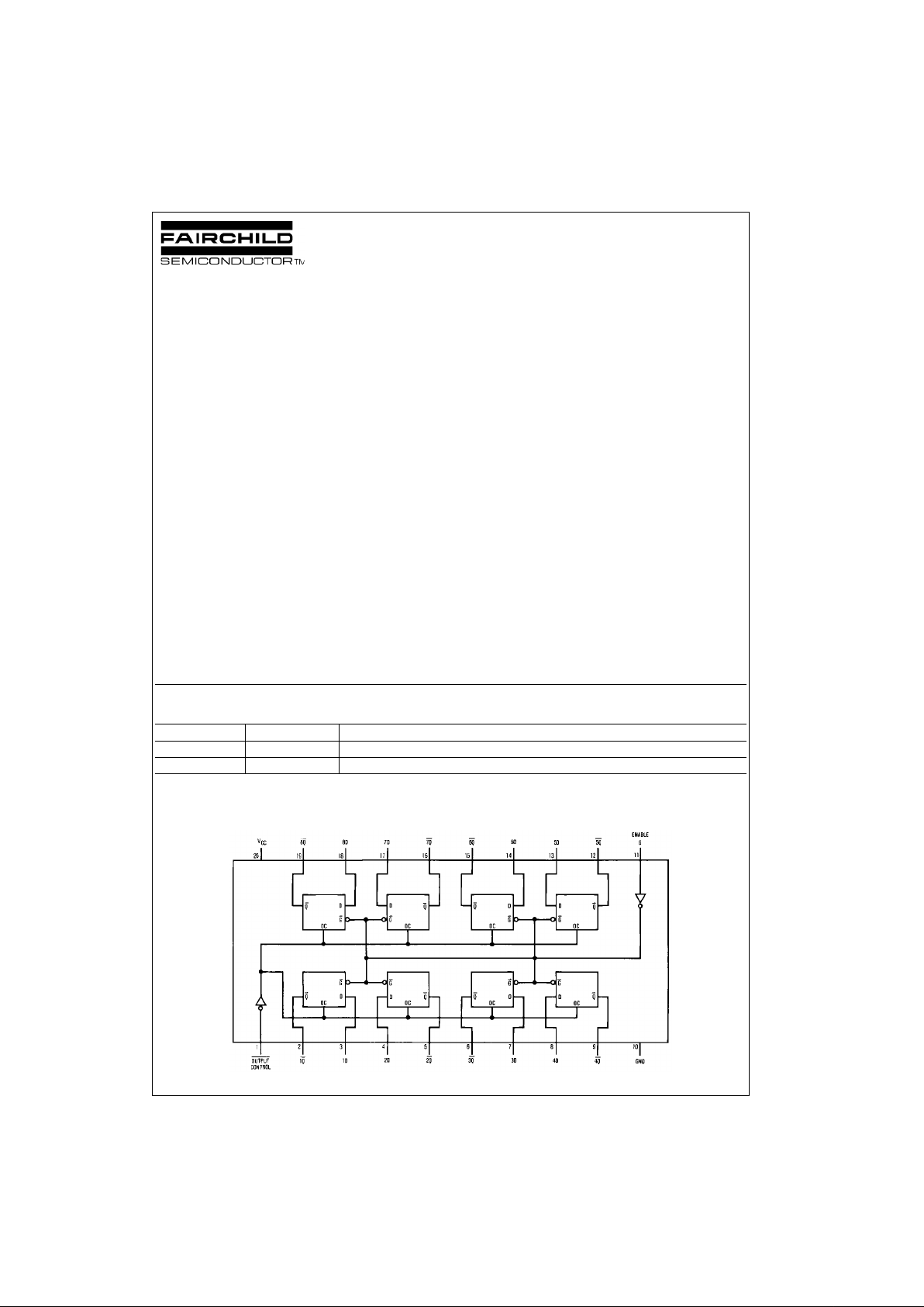
Connection Diagram
Order Number Package Number Package Description
DM74ALS533WM M20B 20-Lead Small Outline Integrated Circuit (SOIC), JEDEC MS-013, 0.300 Wide
DM74ALS533N N20A 20-Lead Plastic Dual-In-Line Package (PDIP), JEDEC MS-001, 0.300 Wide

www.fairchildsemi.com 2
DM74ALS533
Function Table
L = LOW State
H = HIGH State
X = Don’t Care
Z = High Impedance State
Q
0
= Previous Condit ion of Q
Logic Diagram
Output Enable D Output
Control G Q
LHHL
LHLH
LLXQ
0
HXXZ
 Loading...