


MSC1210
Analog-to-Digital Converter
with 8051 Microcontroller and Flash Memory
User’s Guide
December 2002
SBAU077

IMPORTANT NOTICE
Texas Instruments Incorporated and its subsidiaries (TI) reserve the right to make corrections, modifications, enhancements, improvements, and other changes to its products and services at any time and to discontinue any product or service without notice. Customers should obtain the latest relevant information before placing orders and should verify that such information is current and complete. All products are sold subject to TI’s terms and conditions of sale supplied at the time of order acknowledgment.
TI warrants performance of its hardware products to the specifications applicable at the time of sale in accordance with TI’s standard warranty. Testing and other quality control techniques are used to the extent TI deems necessary to support this warranty. Except where mandated by government requirements, testing of all parameters of each product is not necessarily performed.
TI assumes no liability for applications assistance or customer product design. Customers are responsible for their products and applications using TI components. To minimize the risks associated with customer products and applications, customers should provide adequate design and operating safeguards.
TI does not warrant or represent that any license, either express or implied, is granted under any TI patent right, copyright, mask work right, or other TI intellectual property right relating to any combination, machine, or process in which TI products or services are used. Information published by TI regarding third−party products or services does not constitute a license from TI to use such products or services or a warranty or endorsement thereof. Use of such information may require a license from a third party under the patents or other intellectual property of the third party, or a license from TI under the patents or other intellectual property of TI.
Reproduction of information in TI data books or data sheets is permissible only if reproduction is without alteration and is accompanied by all associated warranties, conditions, limitations, and notices. Reproduction of this information with alteration is an unfair and deceptive business practice. TI is not responsible or liable for such altered documentation.
Resale of TI products or services with statements different from or beyond the parameters stated by TI for that product or service voids all express and any implied warranties for the associated TI product or service and is an unfair and deceptive business practice. TI is not responsible or liable for any such statements.
Mailing Address:
Texas Instruments
Post Office Box 655303
Dallas, Texas 75265
Copyright 2002, Texas Instruments Incorporated

Contents
Contents
1 Introduction to the MSC1210 . . . . . . . . . . . . . . . . . . . . . . . . . . . . . . . . . . . . . . . . . . . . . . . . . . . . . |
1-1 |
||
1.1 |
MSC1210 Description . . . . . . . . . . . . . . . . . . . . . . . . . . . . . . . . . . . . . . . . . . . . . . . . . . . . . . . |
1-2 |
|
1.2 |
MSC1210 Pin-Out . . . . . . . . . . . . . . . . . . . . . . . . . . . . . . . . . . . . . . . . . . . . . . . . . . . . . . . . . . |
1-3 |
|
|
1.2.1 I/O Ports (P0, P1, P2, and P3) . . . . . . . . . . . . . . . . . . . . . . . . . . . . . . . . . . . . . . . . |
1-6 |
|
|
1.2.2 Oscillator Inputs (XTAL1 and XTAL2) . . . . . . . . . . . . . . . . . . . . . . . . . . . . . . . . . . . |
1-9 |
|
|
1.2.3 |
Reset Line (RST) . . . . . . . . . . . . . . . . . . . . . . . . . . . . . . . . . . . . . . . . . . . . . . . . . . . |
1-10 |
|
1.2.4 Address Latch Enable (ALE) . . . . . . . . . . . . . . . . . . . . . . . . . . . . . . . . . . . . . . . . . |
1-10 |
|
|
1.2.5 Program Store Enable (PSEN) . . . . . . . . . . . . . . . . . . . . . . . . . . . . . . . . . . . . . . . |
1-10 |
|
|
1.2.6 |
External Access (EA) . . . . . . . . . . . . . . . . . . . . . . . . . . . . . . . . . . . . . . . . . . . . . . . |
1-11 |
1.3 |
Enhanced 8051 Core . . . . . . . . . . . . . . . . . . . . . . . . . . . . . . . . . . . . . . . . . . . . . . . . . . . . . . |
1-12 |
|
1.4 |
Family Device Compatibility . . . . . . . . . . . . . . . . . . . . . . . . . . . . . . . . . . . . . . . . . . . . . . . . . |
1-13 |
|
1.5 |
Flash Memory . . . . . . . . . . . . . . . . . . . . . . . . . . . . . . . . . . . . . . . . . . . . . . . . . . . . . . . . . . . . . |
1-13 |
|
1.6 |
High Performance Analog Functions . . . . . . . . . . . . . . . . . . . . . . . . . . . . . . . . . . . . . . . . . |
1-13 |
|
1.7 |
High-Performance Peripherals . . . . . . . . . . . . . . . . . . . . . . . . . . . . . . . . . . . . . . . . . . . . . . |
1-14 |
|
2 MSC1210 Memory Organization . . . . . . . . . . . . . . . . . . . . . . . . . . . . . . . . . . . . . . . . . . . . . . . . . . |
2-1 |
||
2.1 |
Description . . . . . . . . . . . . . . . . . . . . . . . . . . . . . . . . . . . . . . . . . . . . . . . . . . . . . . . . . . . . . . . . |
2-2 |
|
2.2 |
Program Memory . . . . . . . . . . . . . . . . . . . . . . . . . . . . . . . . . . . . . . . . . . . . . . . . . . . . . . . . . . . |
2-2 |
|
2.3 |
Data Memory . . . . . . . . . . . . . . . . . . . . . . . . . . . . . . . . . . . . . . . . . . . . . . . . . . . . . . . . . . . . . . |
2-4 |
|
|
2.3.1 On-Chip Extended Static RAM (SRAM) . . . . . . . . . . . . . . . . . . . . . . . . . . . . . . . . . |
2-4 |
|
|
2.3.2 On-Chip Flash Data Memory . . . . . . . . . . . . . . . . . . . . . . . . . . . . . . . . . . . . . . . . . . |
2-5 |
|
|
2.3.3 |
External Data Memory . . . . . . . . . . . . . . . . . . . . . . . . . . . . . . . . . . . . . . . . . . . . . . . |
2-5 |
2.4 |
Internal RAM . . . . . . . . . . . . . . . . . . . . . . . . . . . . . . . . . . . . . . . . . . . . . . . . . . . . . . . . . . . . . . . |
2-6 |
|
|
2.4.1 |
The Stack . . . . . . . . . . . . . . . . . . . . . . . . . . . . . . . . . . . . . . . . . . . . . . . . . . . . . . . . . . |
2-7 |
|
2.4.2 |
Register Banks . . . . . . . . . . . . . . . . . . . . . . . . . . . . . . . . . . . . . . . . . . . . . . . . . . . . . . |
2-7 |
|
2.4.3 |
Bit Memory . . . . . . . . . . . . . . . . . . . . . . . . . . . . . . . . . . . . . . . . . . . . . . . . . . . . . . . . . |
2-8 |
|
2.4.4 Special Function Register (SFR) Memory . . . . . . . . . . . . . . . . . . . . . . . . . . . . . . |
2-10 |
|
3 Special Function Registers (SFRs) . . . . . . . . . . . . . . . . . . . . . . . . . . . . . . . . . . . . . . . . . . . . . . . . 3-1
3.1 |
Description . . . . . . . . . . . . . . . . . . . . . . . . . . . . . . . . . . . . . . . . . . . . . . . . . . . . . . . . . . . . . . . . |
3-2 |
3.2 |
Referencing SFRs . . . . . . . . . . . . . . . . . . . . . . . . . . . . . . . . . . . . . . . . . . . . . . . . . . . . . . . . . . |
3-3 |
|
3.2.1 Referencing Bits of SFRs . . . . . . . . . . . . . . . . . . . . . . . . . . . . . . . . . . . . . . . . . . . . . |
3-3 |
3.3 |
Bit−Addressable SFRs . . . . . . . . . . . . . . . . . . . . . . . . . . . . . . . . . . . . . . . . . . . . . . . . . . . . . . |
3-4 |
3.4 |
SFR Types . . . . . . . . . . . . . . . . . . . . . . . . . . . . . . . . . . . . . . . . . . . . . . . . . . . . . . . . . . . . . . . . . |
3-4 |
3.5 |
SFR Definitions . . . . . . . . . . . . . . . . . . . . . . . . . . . . . . . . . . . . . . . . . . . . . . . . . . . . . . . . . . . . . |
3-5 |
4 Basic Registers . . . . . . . . . . . . . . . . . . . . . . . . . . . . . . . . . . . . . . . . . . . . . . . . . . . . . . . . . . . . . . . . . |
4-1 |
|
4.1 Description . . . . . . . . . . . . . . . . . . . . . . . . . . . . . . . . . . . . . . . . . . . . . . . . . . . . . . . . . . . . . . . . 4-2
4.2 Accumulator . . . . . . . . . . . . . . . . . . . . . . . . . . . . . . . . . . . . . . . . . . . . . . . . . . . . . . . . . . . . . . . 4-2
4.3 R Registers . . . . . . . . . . . . . . . . . . . . . . . . . . . . . . . . . . . . . . . . . . . . . . . . . . . . . . . . . . . . . . . . 4-2
4.4 B Register . . . . . . . . . . . . . . . . . . . . . . . . . . . . . . . . . . . . . . . . . . . . . . . . . . . . . . . . . . . . . . . . . 4-3
4.5 Program Counter (PC) . . . . . . . . . . . . . . . . . . . . . . . . . . . . . . . . . . . . . . . . . . . . . . . . . . . . . . 4-3
4.6 Data Pointer (DPTR0/DPTR1) . . . . . . . . . . . . . . . . . . . . . . . . . . . . . . . . . . . . . . . . . . . . . . . . 4-4
4.7 Stack Pointer (SP) . . . . . . . . . . . . . . . . . . . . . . . . . . . . . . . . . . . . . . . . . . . . . . . . . . . . . . . . . . 4-4
Contents i

Contents
5 Addressing Modes . . . . . . . . . . . . . . . . . . . . . . . . . . . . . . . . . . . . . . . . . . . . . . . . . . . . . . . . . . . . . . |
5-1 |
5.1 Description . . . . . . . . . . . . . . . . . . . . . . . . . . . . . . . . . . . . . . . . . . . . . . . . . . . . . . . . . . . . . . . . 5-2
5.2 Immediate Addressing . . . . . . . . . . . . . . . . . . . . . . . . . . . . . . . . . . . . . . . . . . . . . . . . . . . . . . 5-2
5.3 Direct Addressing . . . . . . . . . . . . . . . . . . . . . . . . . . . . . . . . . . . . . . . . . . . . . . . . . . . . . . . . . . . 5-3
5.4 Indirect Addressing . . . . . . . . . . . . . . . . . . . . . . . . . . . . . . . . . . . . . . . . . . . . . . . . . . . . . . . . . 5-4
5.5 External Direct Addressing . . . . . . . . . . . . . . . . . . . . . . . . . . . . . . . . . . . . . . . . . . . . . . . . . . . 5-5
5.6 External Indirect Addressing . . . . . . . . . . . . . . . . . . . . . . . . . . . . . . . . . . . . . . . . . . . . . . . . . 5-6
5.7 Code Indirect Adressing . . . . . . . . . . . . . . . . . . . . . . . . . . . . . . . . . . . . . . . . . . . . . . . . . . . . . 5-6
6 Program Flow . . . . . . . . . . . . . . . . . . . . . . . . . . . . . . . . . . . . . . . . . . . . . . . . . . . . . . . . . . . . . . . . . . . |
6-1 |
6.1 Description . . . . . . . . . . . . . . . . . . . . . . . . . . . . . . . . . . . . . . . . . . . . . . . . . . . . . . . . . . . . . . . . 6-2
6.2 Conditional Branching . . . . . . . . . . . . . . . . . . . . . . . . . . . . . . . . . . . . . . . . . . . . . . . . . . . . . . . 6-2
6.3 Direct Jumps . . . . . . . . . . . . . . . . . . . . . . . . . . . . . . . . . . . . . . . . . . . . . . . . . . . . . . . . . . . . . . . 6-2
6.4 Direct Calls . . . . . . . . . . . . . . . . . . . . . . . . . . . . . . . . . . . . . . . . . . . . . . . . . . . . . . . . . . . . . . . . 6-4
6.5 Returns From Routines . . . . . . . . . . . . . . . . . . . . . . . . . . . . . . . . . . . . . . . . . . . . . . . . . . . . . . 6-4
6.6 Interrupts . . . . . . . . . . . . . . . . . . . . . . . . . . . . . . . . . . . . . . . . . . . . . . . . . . . . . . . . . . . . . . . . . . 6-4
7 System Timing . . . . . . . . . . . . . . . . . . . . . . . . . . . . . . . . . . . . . . . . . . . . . . . . . . . . . . . . . . . . . . . . . . |
7-1 |
||
7.1 |
Description . . . . . . . . . . . . . . . . . . . . . . . . . . . . . . . . . . . . . . . . . . . . . . . . . . . . . . . . . . . . . . . . |
7-2 |
|
7.2 |
System Timers . . . . . . . . . . . . . . . . . . . . . . . . . . . . . . . . . . . . . . . . . . . . . . . . . . . . . . . . . . . . . |
7-4 |
|
|
7.2.1 |
Microseconds Timer . . . . . . . . . . . . . . . . . . . . . . . . . . . . . . . . . . . . . . . . . . . . . . . . . |
7-6 |
|
7.2.2 |
Milliseconds Timer . . . . . . . . . . . . . . . . . . . . . . . . . . . . . . . . . . . . . . . . . . . . . . . . . . . |
7-6 |
7.3 |
Startup Timing . . . . . . . . . . . . . . . . . . . . . . . . . . . . . . . . . . . . . . . . . . . . . . . . . . . . . . . . . . . . . |
7-9 |
|
|
7.3.1 Normal-Mode Power-On Reset Timing . . . . . . . . . . . . . . . . . . . . . . . . . . . . . . . . . |
7-9 |
|
|
7.3.2 Flash Programming Mode Power-On Reset Timing . . . . . . . . . . . . . . . . . . . . . . |
7-9 |
|
8 Timers . . . . . . |
. . . . . . . . . . . . . . . . . . . . . . . . . . . . . . . . . . . . . . . . . . . . . . . . . . . . . . . . . . . . . . . . . . . . |
8-1 |
|
8.1 |
Description . . . . . . . . . . . . . . . . . . . . . . . . . . . . . . . . . . . . . . . . . . . . . . . . . . . . . . . . . . . . . . . . |
8-2 |
|
8.2 |
How Does a Timer Count? . . . . . . . . . . . . . . . . . . . . . . . . . . . . . . . . . . . . . . . . . . . . . . . . . . . |
8-2 |
|
8.3 |
Using Timers to Measure Time . . . . . . . . . . . . . . . . . . . . . . . . . . . . . . . . . . . . . . . . . . . . . . . |
8-2 |
|
|
8.3.1 How Long Does a Timer Take to Count? . . . . . . . . . . . . . . . . . . . . . . . . . . . . . . . . |
8-2 |
|
|
8.3.2 |
Timer SFRs . . . . . . . . . . . . . . . . . . . . . . . . . . . . . . . . . . . . . . . . . . . . . . . . . . . . . . . . . |
8-4 |
|
8.3.3 |
TMOD SFR . . . . . . . . . . . . . . . . . . . . . . . . . . . . . . . . . . . . . . . . . . . . . . . . . . . . . . . . . |
8-5 |
|
8.3.4 |
TCON SFR . . . . . . . . . . . . . . . . . . . . . . . . . . . . . . . . . . . . . . . . . . . . . . . . . . . . . . . . . |
8-8 |
|
8.3.5 |
Initializing a Timer . . . . . . . . . . . . . . . . . . . . . . . . . . . . . . . . . . . . . . . . . . . . . . . . . . . |
8-9 |
|
8.3.6 |
Reading the Timer . . . . . . . . . . . . . . . . . . . . . . . . . . . . . . . . . . . . . . . . . . . . . . . . . . . |
8-9 |
|
8.3.7 Timing the Length of Events . . . . . . . . . . . . . . . . . . . . . . . . . . . . . . . . . . . . . . . . . |
8-11 |
|
8.4 |
Using Timers as Event Counters . . . . . . . . . . . . . . . . . . . . . . . . . . . . . . . . . . . . . . . . . . . . . |
8-12 |
|
8.5 |
Using Timer 2 . . . . . . . . . . . . . . . . . . . . . . . . . . . . . . . . . . . . . . . . . . . . . . . . . . . . . . . . . . . . . |
8-13 |
|
|
8.5.1 |
T2CON SFR . . . . . . . . . . . . . . . . . . . . . . . . . . . . . . . . . . . . . . . . . . . . . . . . . . . . . . . |
8-13 |
|
8.5.2 Timer 2 in Auto-Reload Mode . . . . . . . . . . . . . . . . . . . . . . . . . . . . . . . . . . . . . . . . |
8-14 |
|
|
8.5.3 Timer 2 in Capture Mode . . . . . . . . . . . . . . . . . . . . . . . . . . . . . . . . . . . . . . . . . . . . |
8-15 |
|
|
8.5.4 Timer 2 as a Baud Rate Generator . . . . . . . . . . . . . . . . . . . . . . . . . . . . . . . . . . . . |
8-16 |
|
9 Serial Communication . . . . . . . . . . . . . . . . . . . . . . . . . . . . . . . . . . . . . . . . . . . . . . . . . . . . . . . . . . . |
9-1 |
|
9.1 |
Description . . . . . . . . . . . . . . . . . . . . . . . . . . . . . . . . . . . . . . . . . . . . . . . . . . . . . . . . . . . . . . . . |
9-2 |
9.2 |
Setting the Serial Port Mode . . . . . . . . . . . . . . . . . . . . . . . . . . . . . . . . . . . . . . . . . . . . . . . . . |
9-3 |
|
9.2.1 Serial Mode 0: Synchronous Half-Duplex . . . . . . . . . . . . . . . . . . . . . . . . . . . . . . . |
9-5 |
|
9.2.2 Serial Mode 1: Asynchronous Full-Duplex . . . . . . . . . . . . . . . . . . . . . . . . . . . . . . |
9-6 |
|
9.2.3 Serial Mode 2: Asynchronous Full-Duplex . . . . . . . . . . . . . . . . . . . . . . . . . . . . . . |
9-9 |
|
9.2.4 Serial Mode 3: Asynchronous Full-Duplex . . . . . . . . . . . . . . . . . . . . . . . . . . . . . |
9-11 |
9.3 |
Setting the Serial Port Baud Rate . . . . . . . . . . . . . . . . . . . . . . . . . . . . . . . . . . . . . . . . . . . . |
9-13 |
9.4 |
Writing to the Serial Port . . . . . . . . . . . . . . . . . . . . . . . . . . . . . . . . . . . . . . . . . . . . . . . . . . . . |
9-15 |
9.5 |
Reading the Serial Port . . . . . . . . . . . . . . . . . . . . . . . . . . . . . . . . . . . . . . . . . . . . . . . . . . . . . |
9-16 |
ii

Contents
10 Interrupts . . . . . . . . . . . . . . . . . . . . . . . . . . . . . . . . . . . . . . . . . . . . . . . . . . . . . . . . . . . . . . . . . . . . . . |
10-1 |
10.1 Description . . . . . . . . . . . . . . . . . . . . . . . . . . . . . . . . . . . . . . . . . . . . . . . . . . . . . . . . . . . . . . . 10-2 10.2 Events That Can Trigger Interrupts . . . . . . . . . . . . . . . . . . . . . . . . . . . . . . . . . . . . . . . . . . . 10-3 10.3 Enabling Interrupts . . . . . . . . . . . . . . . . . . . . . . . . . . . . . . . . . . . . . . . . . . . . . . . . . . . . . . . . . 10-5 10.4 Polling Sequence . . . . . . . . . . . . . . . . . . . . . . . . . . . . . . . . . . . . . . . . . . . . . . . . . . . . . . . . . . 10-6 10.5 Interrupt Priorities . . . . . . . . . . . . . . . . . . . . . . . . . . . . . . . . . . . . . . . . . . . . . . . . . . . . . . . . . . 10-7 10.6 Interrupt Triggering . . . . . . . . . . . . . . . . . . . . . . . . . . . . . . . . . . . . . . . . . . . . . . . . . . . . . . . . 10-8 10.7 Exiting Interrupts . . . . . . . . . . . . . . . . . . . . . . . . . . . . . . . . . . . . . . . . . . . . . . . . . . . . . . . . . . 10-8 10.8 Types of Interrupts . . . . . . . . . . . . . . . . . . . . . . . . . . . . . . . . . . . . . . . . . . . . . . . . . . . . . . . . . 10-9
10.8.1 Serial Interrupts . . . . . . . . . . . . . . . . . . . . . . . . . . . . . . . . . . . . . . . . . . . . . . . . . . . . 10-9 10.8.2 External Interrupts . . . . . . . . . . . . . . . . . . . . . . . . . . . . . . . . . . . . . . . . . . . . . . . . . . 10-9 10.8.3 Timer Interrupts . . . . . . . . . . . . . . . . . . . . . . . . . . . . . . . . . . . . . . . . . . . . . . . . . . . 10-11 10.8.4 Watchdog Interrupt . . . . . . . . . . . . . . . . . . . . . . . . . . . . . . . . . . . . . . . . . . . . . . . . 10-11 10.8.5 Auxiliary Interrupts . . . . . . . . . . . . . . . . . . . . . . . . . . . . . . . . . . . . . . . . . . . . . . . . . 10-11
10.9 Waking Up from Idle Mode . . . . . . . . . . . . . . . . . . . . . . . . . . . . . . . . . . . . . . . . . . . . . . . . . 10-15 10.10 Register Protection . . . . . . . . . . . . . . . . . . . . . . . . . . . . . . . . . . . . . . . . . . . . . . . . . . . . . . . 10-16 10.11 Common Problems with Interrupts . . . . . . . . . . . . . . . . . . . . . . . . . . . . . . . . . . . . . . . . . . 10-18
11 |
Pulse Width Modulator/Tone Generator . . . . . . . . . . . . . . . . . . . . . . . . . . . . . . . . . . . . . . . . . . |
11-1 |
|
|
11.1 |
Description . . . . . . . . . . . . . . . . . . . . . . . . . . . . . . . . . . . . . . . . . . . . . . . . . . . . . . . . . . . . . . . |
11-2 |
|
11.2 |
Tone Generator . . . . . . . . . . . . . . . . . . . . . . . . . . . . . . . . . . . . . . . . . . . . . . . . . . . . . . . . . . . |
11-3 |
|
|
11.2.1 Tone Generator Waveforms . . . . . . . . . . . . . . . . . . . . . . . . . . . . . . . . . . . . . . . . . . |
11-4 |
|
11.3 |
PWM Generator . . . . . . . . . . . . . . . . . . . . . . . . . . . . . . . . . . . . . . . . . . . . . . . . . . . . . . . . . . . |
11-5 |
|
|
11.3.1 Example of PWM Tone Generation . . . . . . . . . . . . . . . . . . . . . . . . . . . . . . . . . . . |
11-8 |
|
|
11.3.2 Example of PWM Tone Generation Idling . . . . . . . . . . . . . . . . . . . . . . . . . . . . . . |
11-9 |
|
|
11.3.3 Example of Updating PWM . . . . . . . . . . . . . . . . . . . . . . . . . . . . . . . . . . . . . . . . . |
11-11 |
12 |
Analog-to-Digital Converter . . . . . . . . . . . . . . . . . . . . . . . . . . . . . . . . . . . . . . . . . . . . . . . . . . . . . |
12-1 |
|
12.1 Description . . . . . . . . . . . . . . . . . . . . . . . . . . . . . . . . . . . . . . . . . . . . . . . . . . . . . . . . . . . . . . . 12-2 12.2 Input Multiplexer . . . . . . . . . . . . . . . . . . . . . . . . . . . . . . . . . . . . . . . . . . . . . . . . . . . . . . . . . . . 12-3 12.3 Temperature Sensor . . . . . . . . . . . . . . . . . . . . . . . . . . . . . . . . . . . . . . . . . . . . . . . . . . . . . . . 12-5 12.4 Burnout Current Sources . . . . . . . . . . . . . . . . . . . . . . . . . . . . . . . . . . . . . . . . . . . . . . . . . . . 12-7 12.5 Input Buffer . . . . . . . . . . . . . . . . . . . . . . . . . . . . . . . . . . . . . . . . . . . . . . . . . . . . . . . . . . . . . . . 12-8 12.6 Analog Input . . . . . . . . . . . . . . . . . . . . . . . . . . . . . . . . . . . . . . . . . . . . . . . . . . . . . . . . . . . . . . 12-8 12.7 Programmable Gain Amplifier (PGA) . . . . . . . . . . . . . . . . . . . . . . . . . . . . . . . . . . . . . . . . . 12-9 12.8 Offset DAC . . . . . . . . . . . . . . . . . . . . . . . . . . . . . . . . . . . . . . . . . . . . . . . . . . . . . . . . . . . . . . 12-10 12.9 Modulator . . . . . . . . . . . . . . . . . . . . . . . . . . . . . . . . . . . . . . . . . . . . . . . . . . . . . . . . . . . . . . . 12-10 12.10 Calibration . . . . . . . . . . . . . . . . . . . . . . . . . . . . . . . . . . . . . . . . . . . . . . . . . . . . . . . . . . . . . . . 12-11 12.11 Digital Filter . . . . . . . . . . . . . . . . . . . . . . . . . . . . . . . . . . . . . . . . . . . . . . . . . . . . . . . . . . . . . . 12-12
12.11.1 Multiplexing Channels . . . . . . . . . . . . . . . . . . . . . . . . . . . . . . . . . . . . . . . . . . . . . . 12-14 12.12 Voltage Reference . . . . . . . . . . . . . . . . . . . . . . . . . . . . . . . . . . . . . . . . . . . . . . . . . . . . . . . . 12-15 12.13 Summation/Shifter Register . . . . . . . . . . . . . . . . . . . . . . . . . . . . . . . . . . . . . . . . . . . . . . . . 12-16 12.13.1 Manual Summation Mode . . . . . . . . . . . . . . . . . . . . . . . . . . . . . . . . . . . . . . . . . . 12-18 12.13.2 ADC Summation Mode . . . . . . . . . . . . . . . . . . . . . . . . . . . . . . . . . . . . . . . . . . . . . 12-18 12.13.3 Manual Shift (Divide) Mode . . . . . . . . . . . . . . . . . . . . . . . . . . . . . . . . . . . . . . . . . 12-19 12.13.4 ADC Summation with Shift (Divide) Mode . . . . . . . . . . . . . . . . . . . . . . . . . . . . . 12-19 12.14 Interrupt-Driven ADC Sampling . . . . . . . . . . . . . . . . . . . . . . . . . . . . . . . . . . . . . . . . . . . . . 12-20
12.15 Syncronizing Multiple MSC1210 Devices . . . . . . . . . . . . . . . . . . . . . . . . . . . . . . . . . . . . 12-22 12.16 Ratiometric Measurements . . . . . . . . . . . . . . . . . . . . . . . . . . . . . . . . . . . . . . . . . . . . . . . . 12-24 12.16.1 Differential Vref . . . . . . . . . . . . . . . . . . . . . . . . . . . . . . . . . . . . . . . . . . . . . . . . . . . . 12-25
Contents iii

Contents
13 Serial Peripheral Interface (SPI) . . . . . . . . . . . . . . . . . . . . . . . . . . . . . . . . . . . . . . . . . . . . . . . . . . 13-1
|
13.1 |
Description . . . . . . . . . . . . . . . . . . . . . . . . . . . . . . . . . . . . . . . . . . . . . . . . . . . . . . . . . . . . . . . |
13-2 |
|
|
13.2 |
Functional Description . . . . . . . . . . . . . . . . . . . . . . . . . . . . . . . . . . . . . . . . . . . . . . . . . . . . . . |
13-2 |
|
|
13.3 |
Clock Phase and Polarity Controls . . . . . . . . . . . . . . . . . . . . . . . . . . . . . . . . . . . . . . . . . . . |
13-4 |
|
|
13.4 |
SPI Signals . . . . . . . . . . . . . . . . . . . . . . . . . . . . . . . . . . . . . . . . . . . . . . . . . . . . . . . . . . . . . . . |
13-5 |
|
|
|
13.4.1 Master In Slave Out . . . . . . . . . . . . . . . . . . . . . . . . . . . . . . . . . . . . . . . . . . . . . . . . . |
13-5 |
|
|
|
13.4.2 Master Out Slave In . . . . . . . . . . . . . . . . . . . . . . . . . . . . . . . . . . . . . . . . . . . . . . . . . |
13-5 |
|
|
|
13.4.3 |
Serial Clock . . . . . . . . . . . . . . . . . . . . . . . . . . . . . . . . . . . . . . . . . . . . . . . . . . . . . . . . |
13-5 |
|
|
13.4.4 |
Slave Select . . . . . . . . . . . . . . . . . . . . . . . . . . . . . . . . . . . . . . . . . . . . . . . . . . . . . . . |
13-5 |
|
13.5 |
SPI System Errors . . . . . . . . . . . . . . . . . . . . . . . . . . . . . . . . . . . . . . . . . . . . . . . . . . . . . . . . . |
13-6 |
|
|
13.6 |
Data Transfers . . . . . . . . . . . . . . . . . . . . . . . . . . . . . . . . . . . . . . . . . . . . . . . . . . . . . . . . . . . . |
13-7 |
|
|
13.7 |
FIFO Operation . . . . . . . . . . . . . . . . . . . . . . . . . . . . . . . . . . . . . . . . . . . . . . . . . . . . . . . . . . . |
13-9 |
|
|
13.8 |
Code Examples . . . . . . . . . . . . . . . . . . . . . . . . . . . . . . . . . . . . . . . . . . . . . . . . . . . . . . . . . . |
13-10 |
|
|
|
13.8.1 SPI Master Transfer in Double-Buffer Mode using Interrupt Polling . . . . . . . |
13-10 |
|
|
|
13.8.2 SPI Master Transfer in FIFO Mode using Interrupts . . . . . . . . . . . . . . . . . . . . |
13-11 |
|
14 |
Additional MSC1210 Hardware . . . . . . . . . . . . . . . . . . . . . . . . . . . . . . . . . . . . . . . . . . . . . . . . . . |
14-1 |
||
|
14.1 |
Description . . . . . . . . . . . . . . . . . . . . . . . . . . . . . . . . . . . . . . . . . . . . . . . . . . . . . . . . . . . . . . . |
14-2 |
|
|
14.2 |
Low-Voltage Detect . . . . . . . . . . . . . . . . . . . . . . . . . . . . . . . . . . . . . . . . . . . . . . . . . . . . . . . . |
14-2 |
|
|
|
14.2.1 |
Power Supply . . . . . . . . . . . . . . . . . . . . . . . . . . . . . . . . . . . . . . . . . . . . . . . . . . . . . . |
14-3 |
|
14.3 |
Watchdog Timer . . . . . . . . . . . . . . . . . . . . . . . . . . . . . . . . . . . . . . . . . . . . . . . . . . . . . . . . . . . |
14-4 |
|
|
|
14.3.1 Watchdog Timer Hardware Configuration . . . . . . . . . . . . . . . . . . . . . . . . . . . . . . |
14-4 |
|
|
|
14.3.2 |
Enabling Watchdog Timer . . . . . . . . . . . . . . . . . . . . . . . . . . . . . . . . . . . . . . . . . . . |
14-5 |
|
|
14.3.3 Resetting the Watchdog Timer . . . . . . . . . . . . . . . . . . . . . . . . . . . . . . . . . . . . . . . |
14-7 |
|
|
|
14.3.4 |
Disabling Watchdog Timer . . . . . . . . . . . . . . . . . . . . . . . . . . . . . . . . . . . . . . . . . . . |
14-8 |
|
|
14.3.5 |
Watchdog Timeout/Activation . . . . . . . . . . . . . . . . . . . . . . . . . . . . . . . . . . . . . . . . |
14-8 |
15 |
Advanced Topics . . . . . . . . . . . . . . . . . . . . . . . . . . . . . . . . . . . . . . . . . . . . . . . . . . . . . . . . . . . . . . . |
15-1 |
||
|
15.1 |
Hardware Configuration . . . . . . . . . . . . . . . . . . . . . . . . . . . . . . . . . . . . . . . . . . . . . . . . . . . . |
15-2 |
|
|
|
15.1.1 |
Hardware Configuration Registers . . . . . . . . . . . . . . . . . . . . . . . . . . . . . . . . . . . . |
15-2 |
|
|
15.1.2 |
Hardware Configuration Memory . . . . . . . . . . . . . . . . . . . . . . . . . . . . . . . . . . . . . |
15-5 |
|
|
15.1.3 Accessing Configuration Memory in a User Program . . . . . . . . . . . . . . . . . . . . |
15-5 |
|
|
15.2 |
Advanced Flash Memory . . . . . . . . . . . . . . . . . . . . . . . . . . . . . . . . . . . . . . . . . . . . . . . . . . . |
15-6 |
|
|
|
15.2.1 Write Protecting Flash Program Memory . . . . . . . . . . . . . . . . . . . . . . . . . . . . . . . |
15-6 |
|
|
|
15.2.2 Updating Interrupts with Reset Sector Lock . . . . . . . . . . . . . . . . . . . . . . . . . . . . |
15-6 |
|
|
15.3 |
Breakpoint Generator . . . . . . . . . . . . . . . . . . . . . . . . . . . . . . . . . . . . . . . . . . . . . . . . . . . . . . |
15-7 |
|
|
|
15.3.1 |
Configuring Breakpoints . . . . . . . . . . . . . . . . . . . . . . . . . . . . . . . . . . . . . . . . . . . . . |
15-7 |
|
|
15.3.2 |
Breakpoint Auxiliary Interrupt . . . . . . . . . . . . . . . . . . . . . . . . . . . . . . . . . . . . . . . . . |
15-8 |
|
|
15.3.3 |
Disabling a Breakpoint . . . . . . . . . . . . . . . . . . . . . . . . . . . . . . . . . . . . . . . . . . . . . . |
15-8 |
|
15.4 |
Power Optimization . . . . . . . . . . . . . . . . . . . . . . . . . . . . . . . . . . . . . . . . . . . . . . . . . . . . . . . . |
15-9 |
|
|
15.5 |
Flash Memory as Data Memory . . . . . . . . . . . . . . . . . . . . . . . . . . . . . . . . . . . . . . . . . . . . |
15-10 |
|
|
15.6 |
Advanced Topics and Other Information . . . . . . . . . . . . . . . . . . . . . . . . . . . . . . . . . . . . . |
15-12 |
|
|
|
15.6.1 Serial and Parallel Programming of the MSC1210 . . . . . . . . . . . . . . . . . . . . . |
15-12 |
|
|
|
15.6.2 Debugging Using the MSC1210 Boot ROM Routines . . . . . . . . . . . . . . . . . . . |
15-12 |
|
|
|
15.6.3 Using MSC1210 with Raisonance Development Tools . . . . . . . . . . . . . . . . . . |
15-12 |
|
|
|
15.6.4 Using the MSC1210 Evaluation Module (EVM) . . . . . . . . . . . . . . . . . . . . . . . . |
15-12 |
|
iv

Contents
16 8052 Assembly Language . . . . . . . . . . . . . . . . . . . . . . . . . . . . . . . . . . . . . . . . . . . . . . . . . . . . . . . 16-1
16.1 Description . . . . . . . . . . . . . . . . . . . . . . . . . . . . . . . . . . . . . . . . . . . . . . . . . . . . . . . . . . . . . . . 16-2 16.2 Syntax . . . . . . . . . . . . . . . . . . . . . . . . . . . . . . . . . . . . . . . . . . . . . . . . . . . . . . . . . . . . . . . . . . . 16-2 16.3 Number Bases . . . . . . . . . . . . . . . . . . . . . . . . . . . . . . . . . . . . . . . . . . . . . . . . . . . . . . . . . . . . 16-4 16.4 Expressions . . . . . . . . . . . . . . . . . . . . . . . . . . . . . . . . . . . . . . . . . . . . . . . . . . . . . . . . . . . . . . . 16-4 16.5 Operator Precedence . . . . . . . . . . . . . . . . . . . . . . . . . . . . . . . . . . . . . . . . . . . . . . . . . . . . . . 16-5 16.6 Characters and Character Strings . . . . . . . . . . . . . . . . . . . . . . . . . . . . . . . . . . . . . . . . . . . . 16-5 16.7 Changing Program Flow (LJMP, SJMP, AJMP) . . . . . . . . . . . . . . . . . . . . . . . . . . . . . . . . 16-6 16.8 Subroutines (LCALL, ACALL, RET) . . . . . . . . . . . . . . . . . . . . . . . . . . . . . . . . . . . . . . . . . . 16-7 16.9 Register Assignment (MOV) . . . . . . . . . . . . . . . . . . . . . . . . . . . . . . . . . . . . . . . . . . . . . . . . 16-8 16.10 Incrementing and Decrementing Registers (INC, DEC) . . . . . . . . . . . . . . . . . . . . . . . . 16-11 16.11 Program Loops (DJNZ) . . . . . . . . . . . . . . . . . . . . . . . . . . . . . . . . . . . . . . . . . . . . . . . . . . . . 16-12 16.12 Setting, Clearing, and Moving Bits (SETB, CLR, CPL, MOV) . . . . . . . . . . . . . . . . . . . 16-13 16.13 Bit-Based Decisions and Branching (JB, JBC, JNB, JC, JNC) . . . . . . . . . . . . . . . . . . 16-15 16.14 Value Comparison (CJNE) . . . . . . . . . . . . . . . . . . . . . . . . . . . . . . . . . . . . . . . . . . . . . . . . . 16-16 16.15 Less Than and Greater Than Comparison (CJNE) . . . . . . . . . . . . . . . . . . . . . . . . . . . . 16-17 16.16 Zero and Non-Zero Decisions (JZ/JNZ) . . . . . . . . . . . . . . . . . . . . . . . . . . . . . . . . . . . . . . 16-18 16.17 Performing Additions (ADD, ADDC) . . . . . . . . . . . . . . . . . . . . . . . . . . . . . . . . . . . . . . . . . 16-18 16.18 Performing Subtractions (SUBB) . . . . . . . . . . . . . . . . . . . . . . . . . . . . . . . . . . . . . . . . . . . . 16-20 16.19 Performing Multiplication (MUL) . . . . . . . . . . . . . . . . . . . . . . . . . . . . . . . . . . . . . . . . . . . . 16-21 16.20 Performing Division (DIV) . . . . . . . . . . . . . . . . . . . . . . . . . . . . . . . . . . . . . . . . . . . . . . . . . . 16-22 16.21 Shifting Bits (RR, RRC, RL, RLC) . . . . . . . . . . . . . . . . . . . . . . . . . . . . . . . . . . . . . . . . . . . 16-23 16.22 Bit-Wise Logical Instructions (ANL, ORL, XRL) . . . . . . . . . . . . . . . . . . . . . . . . . . . . . . . 16-24 16.23 Exchanging Register Values (XCH) . . . . . . . . . . . . . . . . . . . . . . . . . . . . . . . . . . . . . . . . . 16-26 16.24 Swapping Accumulator Nibbles (SWAP) . . . . . . . . . . . . . . . . . . . . . . . . . . . . . . . . . . . . . 16-26 16.25 Exchanging Nibbles Between Accumulator and Internal RAM (XCHD) . . . . . . . . . . . 16-26 16.26 Adjusting Accumulator for BCD Addition (DA) . . . . . . . . . . . . . . . . . . . . . . . . . . . . . . . . 16-27 16.27 Using the Stack (PUSH/POP) . . . . . . . . . . . . . . . . . . . . . . . . . . . . . . . . . . . . . . . . . . . . . . 16-28 16.28 Setting the Data Pointer DPTR (MOV DPTR) . . . . . . . . . . . . . . . . . . . . . . . . . . . . . . . . . 16-30 16.29 Reading and Writing External RAM/Data Memory (MOVX) . . . . . . . . . . . . . . . . . . . . . 16-31 16.30 Reading Code Memory/Tables (MOVC) . . . . . . . . . . . . . . . . . . . . . . . . . . . . . . . . . . . . . . 16-32 16.31 Using Jump Tables (JMP @A+DPTR) . . . . . . . . . . . . . . . . . . . . . . . . . . . . . . . . . . . . . . . 16-34
17 Keil Simulator . . . . . . . . . . . . . . . . . . . . . . . . . . . . . . . . . . . . . . . . . . . . . . . . . . . . . . . . . . . . . . . . . . 17-1
17.1 Description . . . . . . . . . . . . . . . . . . . . . . . . . . . . . . . . . . . . . . . . . . . . . . . . . . . . . . . . . . . . . . . 17-2 17.2 Timers . . . . . . . . . . . . . . . . . . . . . . . . . . . . . . . . . . . . . . . . . . . . . . . . . . . . . . . . . . . . . . . . . . . 17-4 17.2.1 Timer 0 & 1 Example . . . . . . . . . . . . . . . . . . . . . . . . . . . . . . . . . . . . . . . . . . . . . . . . 17-5 17.3 Timer 2 . . . . . . . . . . . . . . . . . . . . . . . . . . . . . . . . . . . . . . . . . . . . . . . . . . . . . . . . . . . . . . . . . . 17-11
17.4 Watchdog Timer . . . . . . . . . . . . . . . . . . . . . . . . . . . . . . . . . . . . . . . . . . . . . . . . . . . . . . . . . . 17-12 17.4.1 Watchdog Reset Facility Example . . . . . . . . . . . . . . . . . . . . . . . . . . . . . . . . . . . 17-13 17.5 System Timer . . . . . . . . . . . . . . . . . . . . . . . . . . . . . . . . . . . . . . . . . . . . . . . . . . . . . . . . . . . . 17-16
17.6 Clock Control . . . . . . . . . . . . . . . . . . . . . . . . . . . . . . . . . . . . . . . . . . . . . . . . . . . . . . . . . . . . 17-16 17.7 Analog-to-Digital Converter . . . . . . . . . . . . . . . . . . . . . . . . . . . . . . . . . . . . . . . . . . . . . . . . 17-17 17.8 Summation/Shifter . . . . . . . . . . . . . . . . . . . . . . . . . . . . . . . . . . . . . . . . . . . . . . . . . . . . . . . . 17-20 17.8.1 ADC/Summation/Shifter Example . . . . . . . . . . . . . . . . . . . . . . . . . . . . . . . . . . . . 17-21 17.9 Interrupts . . . . . . . . . . . . . . . . . . . . . . . . . . . . . . . . . . . . . . . . . . . . . . . . . . . . . . . . . . . . . . . . 17-30
17.10 Ports . . . . . . . . . . . . . . . . . . . . . . . . . . . . . . . . . . . . . . . . . . . . . . . . . . . . . . . . . . . . . . . . . . . . 17-31 17.11 Serial Peripheral Interface (SPI) . . . . . . . . . . . . . . . . . . . . . . . . . . . . . . . . . . . . . . . . . . . . 17-32 17.11.1 SPI Sample Code . . . . . . . . . . . . . . . . . . . . . . . . . . . . . . . . . . . . . . . . . . . . . . . . . 17-34 17.12 mVision 2 Debug Program Example . . . . . . . . . . . . . . . . . . . . . . . . . . . . . . . . . . . . . . . . . 17-38
17.13 Serial Port I/O . . . . . . . . . . . . . . . . . . . . . . . . . . . . . . . . . . . . . . . . . . . . . . . . . . . . . . . . . . . . 17-40 17.13.1 Serial Port 0 Operation Mode 1 Example . . . . . . . . . . . . . . . . . . . . . . . . . . . . . 17-42 17.13.2 Transmit Block Baud Rate Computation . . . . . . . . . . . . . . . . . . . . . . . . . . . . . . 17-43 17.13.3 Receive Block Baud Rate Computation . . . . . . . . . . . . . . . . . . . . . . . . . . . . . . . 17-44 17.14 Additional Resource . . . . . . . . . . . . . . . . . . . . . . . . . . . . . . . . . . . . . . . . . . . . . . . . . . . . . . 17-46
Contents v

Contents
A |
Additional Features in the MSC1210 Compared to the 8052 . . . . . . . . . . . . . . . . . . . . . . . . . |
A-1 |
|
|
A.1 |
Additional Features in the MSC1210 Compared to 8052 . . . . . . . . . . . . . . . . . . . . . . . . . |
A-2 |
B |
Clock Timing Diagram . . . . . . . . . . . . . . . . . . . . . . . . . . . . . . . . . . . . . . . . . . . . . . . . . . . . . . . . . . . |
B-1 |
|
|
B.1 |
MSC1210 Timing Chain and Clock Control Diagram . . . . . . . . . . . . . . . . . . . . . . . . . . . . . |
B-2 |
C |
Boot ROM Routines . . . . . . . . . . . . . . . . . . . . . . . . . . . . . . . . . . . . . . . . . . . . . . . . . . . . . . . . . . . . . |
C-1 |
|
|
C.1 |
Description . . . . . . . . . . . . . . . . . . . . . . . . . . . . . . . . . . . . . . . . . . . . . . . . . . . . . . . . . . . . . . . . |
C-2 |
|
|
C.1.1 Note Regarding the put_string Function . . . . . . . . . . . . . . . . . . . . . . . . . . . . . . . . |
C-3 |
D |
8052 Instruction-Set Quick-Reference Guide . . . . . . . . . . . . . . . . . . . . . . . . . . . . . . . . . . . . . . . |
D-1 |
|
|
D.1 |
8052 Instruction-Set Quick-Reference Guide . . . . . . . . . . . . . . . . . . . . . . . . . . . . . . . . . . . |
D-2 |
E |
8052 Instruction Set . . . . . . . . . . . . . . . . . . . . . . . . . . . . . . . . . . . . . . . . . . . . . . . . . . . . . . . . . . . . . |
E-1 |
|
|
E.1 |
Description . . . . . . . . . . . . . . . . . . . . . . . . . . . . . . . . . . . . . . . . . . . . . . . . . . . . . . . . . . . . . . . . |
E-2 |
|
E.2 |
8052 Instruction Set . . . . . . . . . . . . . . . . . . . . . . . . . . . . . . . . . . . . . . . . . . . . . . . . . . . . . . . . . |
E-3 |
F |
Bit-Addressable SFRs (alphabetical) . . . . . . . . . . . . . . . . . . . . . . . . . . . . . . . . . . . . . . . . . . . . . . |
F-1 |
|
|
F.1 |
Bit Addressable SFRs (alphabetical) . . . . . . . . . . . . . . . . . . . . . . . . . . . . . . . . . . . . . . . . . . |
F-2 |
G |
SFRs/Address Cross-Reference Guide (alphabetical) . . . . . . . . . . . . . . . . . . . . . . . . . . . . . . |
G-1 |
|
G.1 SFR/Address Cross-Reference . . . . . . . . . . . . . . . . . . . . . . . . . . . . . . . . . . . . . . . . . . . . . . . G-2
vi

Contents
|
|
|
Figures |
|
|
|
|
|
|
|
|
|
|
|
|
|
|
|
|
|
|
|
|
|
|
|
|
|
|
|
|
|
|
|
1−1. |
MSC1210 Block Diagram . . . . . . . . . . |
. . . . . . . . . . . . . . . . . . . . . . . |
. . . . . . . . . . . . . . . . . . . . . 1-2 |
|
1−2. |
Pin Configuration of the MSC1210 . . |
. . . . . . . . . . . . . . . . . . . . . . . |
. . . . . . . . . . . . . . . . . . . . . 1-3 |
|
1−3. |
MSC1210 Timing Compared to Standard 8051 Timing . . . . . . . . |
. . . . . . . . . . . . . . . . . . . . 1-12 |
|
|
2−1. |
MSC1210 Memory Map . . . . . . . . . . . . |
. . . . . . . . . . . . . . . . . . . . . . . |
. . . . . . . . . . . . . . . . . . . . . 2-2 |
|
2−2. |
MSC1210 Memory Map Register Bank. . . . . . . . . . . . . . . . . . . . . . . . . . . . . . . . . . . . . . . . . . . 2-6 |
|||
7−1. |
Standard 8051 Timing. . . . . . . . . . . . . . . . . . . . . . . . . . . . . . . . . . . . . . . . . . . . . . . . . . . . . . . . . . 7-2 |
|||
7−2. |
MSC1210 Timing Chain and Clock Control . . . . . . . . . . . . . . . . . . |
. . . . . . . . . . . . . . . . . . . . . 7-5 |
|
|
7−3. |
SPI/PWM/Flash Write Timing . . . . . . . |
. . . . . . . . . . . . . . . . . . . . . . . |
. . . . . . . . . . . . . . . . . . . . . 7-5 |
|
7−4. |
System Timing Interrupt Control . . . . . |
. . . . . . . . . . . . . . . . . . . . . . . |
. . . . . . . . . . . . . . . . . . . . . 7-7 |
|
7−5. |
Reset Timing . . . . . . . . . . . . . . . . . . . . . |
. . . . . . . . . . . . . . . . . . . . . . . |
. . . . . . . . . . . . . . . . . . . . . 7-9 |
|
7−6. |
Parallel Flash Programming Power-On Timing (EA is ignored) . |
. . . . . . . . . . . . . . . . . . . . . 7-9 |
|
|
7−7. |
Serial Flash Programming Power-On Timing (EA is ignored) . . . |
. . . . . . . . . . . . . . . . . . . . 7-10 |
|
|
8−1. |
Timer 0/1 Block Diagram for Modes 0 and 1 . . . . . . . . . . . . . . . . . |
. . . . . . . . . . . . . . . . . . . . . 8-6 |
|
|
9−1. |
Serial Port 0 Mode 0 Transmit Timing—High Speed Operation. |
. . . . . . . . . . . . . . . . . . . . .9-6 |
|
|
9−2. |
Serial Port Mode 0 Receive Timing—High Speed Operation. . . . . . . . . . . . . . . . . . . . . . . . .9-6 |
|||
9−3. |
Serial Port Mode 1 Transmit Timing. . . . . . . . . . . . . . . . . . . . . . . . . . . . . . . . . . . . . . . . . . . . . . 9-7 |
|||
9−4. |
Serial Port 0 Mode 1 Receive Timing. |
. . . . . . . . . . . . . . . . . . . . . . . . . . . . . . . . . . . . . . . . . . . . 9-7 |
|
|
9−5. |
Serial Port 0 Mode 2 Transmit Timing. |
. . . . . . . . . . . . . . . . . . . . . . . . . . . . . . . . . . . . . . . . . . . 9-9 |
|
|
9−6. |
Serial Port 0 Mode 2 Receive Timing. |
. . . . . . . . . . . . . . . . . . . . . . . . . . . . . . . . . . . . . . . . . . . 9-10 |
|
|
9−7. |
Serial Port 0 Mode 3 Transmit Timing. |
. . . . . . . . . . . . . . . . . . . . . . . . . . . . . . . . . . . . . . . . . . 9-11 |
|
|
9−8. |
Serial Port 0 Mode 3 Receive Timing. |
. . . . . . . . . . . . . . . . . . . . . . . . . . . . . . . . . . . . . . . . . . . 9-11 |
|
|
11−1. |
Block Diagram . . . . . . . . . . . . . . . . . . . . |
. . . . . . . . . . . . . . . . . . . . . . . |
. . . . . . . . . . . . . . . . . . . . 11-2 |
|
11−2. |
Tone Generator Circuit . . . . . . . . . . . . . |
. . . . . . . . . . . . . . . . . . . . . . . |
. . . . . . . . . . . . . . . . . . . . 11-3 |
|
11−3. |
Timing Diagram of Tone Generator in Staircase Mode . . . . . . . . |
. . . . . . . . . . . . . . . . . . . . 11-4 |
|
|
11−4. |
Timing Diagram of Tone Generator in Square Wave Mode . . . . . |
. . . . . . . . . . . . . . . . . . . . 11-4 |
|
|
11−5. |
Timing Diagram of a PWM Waveform |
. . . . . . . . . . . . . . . . . . . . . . . |
. . . . . . . . . . . . . . . . . . . . 11-6 |
|
11−6. |
PWM Timing . . . . . . . . . . . . . . . . . . . . . |
. . . . . . . . . . . . . . . . . . . . . . . |
. . . . . . . . . . . . . . . . . . . 11-11 |
|
12−1. |
MSC1210 Architecture . . . . . . . . . . . . . |
. . . . . . . . . . . . . . . . . . . . . . . |
. . . . . . . . . . . . . . . . . . . . 12-2 |
|
12−2. |
Input Multiplexer Configuration . . . . . . |
. . . . . . . . . . . . . . . . . . . . . . . |
. . . . . . . . . . . . . . . . . . . . 12-3 |
|
12−3. |
Basic Input Structure of the MSC1210 |
. . . . . . . . . . . . . . . . . . . . . . |
. . . . . . . . . . . . . . . . . . . . 12-8 |
|
12−4. |
Filter Step Responses . . . . . . . . . . . . . |
. . . . . . . . . . . . . . . . . . . . . . . |
. . . . . . . . . . . . . . . . . . . 12-12 |
|
12−5. |
Filter Frequency Responses . . . . . . . . |
. . . . . . . . . . . . . . . . . . . . . . . |
. . . . . . . . . . . . . . . . . . . 12-13 |
|
12−6. |
Circuit Drawing . . . . . . . . . . . . . . . . . . . |
. . . . . . . . . . . . . . . . . . . . . . . |
. . . . . . . . . . . . . . . . . . . 12-24 |
|
13−1. |
SPI block diagram . . . . . . . . . . . . . . . . . |
. . . . . . . . . . . . . . . . . . . . . . . |
. . . . . . . . . . . . . . . . . . . . 13-2 |
|
13−2. |
SPI Clock/Data Timing . . . . . . . . . . . . . |
. . . . . . . . . . . . . . . . . . . . . . . |
. . . . . . . . . . . . . . . . . . . . 13-3 |
|
13−3. |
SPI Reset State . . . . . . . . . . . . . . . . . . . |
. . . . . . . . . . . . . . . . . . . . . . . |
. . . . . . . . . . . . . . . . . . . . 13-7 |
|
13−4. |
SPI FIFO Operation . . . . . . . . . . . . . . . |
. . . . . . . . . . . . . . . . . . . . . . . |
. . . . . . . . . . . . . . . . . . . . 13-9 |
|
14−1. |
Brownout Reset and Low-Voltage Detection . . . . . . . . . . . . . . . . . |
. . . . . . . . . . . . . . . . . . . . 14-2 |
|
|
14−2. |
System Timing Interrupt Control . . . . . |
. . . . . . . . . . . . . . . . . . . . . . . |
. . . . . . . . . . . . . . . . . . . . 14-4 |
|
Contents vii

Contents
16−1. |
Rotate Operations . . . . . . . . . . . . . . . . . . . . . . . . . . . . . . . . . . . . . . . . . . . . . . . . . . . . . . . . . . |
. 16-23 |
17−1. |
Timer/Counter 0 − Mode 2 . . . . . . . . . . . . . . . . . . . . . . . . . . . . . . . . . . . . . . . . . . . . . . . . . . |
. .17-4 |
17−2. |
Timer/Counter 0 . . . . . . . . . . . . . . . . . . . . . . . . . . . . . . . . . . . . . . . . . . . . . . . . . . . . . . . . . . . |
. . 17-5 |
17−3. |
Parallel Port 3 Peripheral . . . . . . . . . . . . . . . . . . . . . . . . . . . . . . . . . . . . . . . . . . . . . . . . . . . . |
. . 17-5 |
17−4. |
Timer/Counter 1 Mode 1 . . . . . . . . . . . . . . . . . . . . . . . . . . . . . . . . . . . . . . . . . . . . . . . . . . . . |
. . 17-6 |
17−5. |
Interrupt System . . . . . . . . . . . . . . . . . . . . . . . . . . . . . . . . . . . . . . . . . . . . . . . . . . . . . . . . . . . |
. . 17-6 |
17−6. |
Timer/Counter 2 . . . . . . . . . . . . . . . . . . . . . . . . . . . . . . . . . . . . . . . . . . . . . . . . . . . . . . . . . . . |
. 17-11 |
17−7. |
Status of Watchdog Peripheral . . . . . . . . . . . . . . . . . . . . . . . . . . . . . . . . . . . . . . . . . . . . . . . |
. 17-12 |
17−8. |
Analog−to−Digital Converter Peripheral . . . . . . . . . . . . . . . . . . . . . . . . . . . . . . . . . . . . . . . |
17.-18 |
17−9. |
Error Message . . . . . . . . . . . . . . . . . . . . . . . . . . . . . . . . . . . . . . . . . . . . . . . . . . . . . . . . . . . . . |
. 17-19 |
17−10. Accumulator/Shifter Peripheral . . . . . . . . . . . . . . . . . . . . . . . . . . . . . . . . . . . . . . . . . . . . . . . |
. 17-20 |
|
17−11. summation/Shifter Peripheral . . . . . . . . . . . . . . . . . . . . . . . . . . . . . . . . . . . . . . . . . . . . . . . . |
. 17-28 |
|
17−12. The ADC Peripheral Mid-Stride a Typical 8-Sample Averaging Block . . . . . . . . . . . . . |
. 17-28 |
|
17−13. List Box for the Interrupt Peripheral . . . . . . . . . . . . . . . . . . . . . . . . . . . . . . . . . . . . . . . . . . . |
. 17-30 |
|
17−14. Parallel Port 0 Contents Display Window . . . . . . . . . . . . . . . . . . . . . . . . . . . . . . . . . . . . . . |
. 17-31 |
|
17−15. Error Message . . . . . . . . . . . . . . . . . . . . . . . . . . . . . . . . . . . . . . . . . . . . . . . . . . . . . . . . . . . . . |
. 17-31 |
|
17−16. SPI Peripheral Window . . . . . . . . . . . . . . . . . . . . . . . . . . . . . . . . . . . . . . . . . . . . . . . . . . . . . |
. 17-32 |
|
17−17. Keil Debugger . . . . . . . . . . . . . . . . . . . . . . . . . . . . . . . . . . . . . . . . . . . . . . . . . . . . . . . . . . . . . |
. 17-39 |
|
17−18. Serial Channel 0 Communication Peripheral . . . . . . . . . . . . . . . . . . . . . . . . . . . . . . . . . . . |
. 17-41 |
|
17−19. Clock Control Peripheral . . . . . . . . . . . . . . . . . . . . . . . . . . . . . . . . . . . . . . . . . . . . . . . . . . . . |
. 17-45 |
|
17−20. USART0 Preipheral . . . . . . . . . . . . . . . . . . . . . . . . . . . . . . . . . . . . . . . . . . . . . . . . . . . . . . . . |
. 17-45 |
|
B−1. |
MSC1210 Timing Chain and Clock Control . . . . . . . . . . . . . . . . . . . . . . . . . . . . . . . . . . . . |
. . . B-2 |
viii
Contents
|
|
|
|
Tables |
|
|
|
|
|
|
|
|
|
|
|
|
|
|
|
|
|
|
|
|
|
|
|
|
|
|
|
|
|
|
|
|
|
|
|
|
|
1−1. |
Pin Descriptions of the MSC1210 . . . . |
. . . . . . . . . . . . . . . . . . . . . . . . . . . . . . . . . . |
. . . . . . . . . 1-4 |
|
|
2−1. |
Program and Data Memory Size. . . . . . . . . . . . . . . . . . . . . . . . . . . . . . . . . . . . . . . . . . . . . . . . . 2-3 |
||||
2−2. |
Program and Data Memory Addresses. |
. . . . . . . . . . . . . . . . . . . . . . . . . . . . . . . . . . . . . . . . . . 2-4 |
|
||
3−1. |
SFR Names and Addresses. . . . . . . . . . . . . . . . . . . . . . . . . . . . . . . . . . . . . . . . . . . . . . . . . . . . 3-2 |
||||
5−1. |
MSC1210 Addressing Modes. |
. . . . . . . . . . . . . . . . . . . . . . . . . . . . . . . . . . . . . . . . . . . . . . . . . . 5-2 |
|
||
7−1. |
Signal Definitions for Reset Timing Diagrams . . . . . . . . . . . . . . . . . . . . . . . . . . . . |
. . . . . . . . 7-10 |
|
||
8−1. |
Timer Conrol SFRs. . . . . . . . . . . . . . . . . . . . . . . . . . . . . . . . . . . . . . . . . . . . . . . . . . . . . . . . . . . . 8-4 |
||||
8−2. |
Timer Modes and Usage . . . . . |
. . . . . . . |
. . . . . . . . . . . . . . . . . . . . . . . . . . . . . . . . . . . |
. . . . . . . . 8-6 |
|
8−3. |
Example of 8-Bit Auto-Reload |
. . . . . . . |
. . . . . . . . . . . . . . . . . . . . . . . . . . . . . . . . . . . |
. . . . . . . . 8-7 |
|
8−4. |
TCON (88h) SFR . . . . . . . . . . . |
. . . . . . . |
. . . . . . . . . . . . . . . . . . . . . . . . . . . . . . . . . . . |
. . . . . . . . 8-8 |
|
9−1. |
SM0 and SM1 Function Definitions. . . . . . . . . . . . . . . . . . . . . . . . . . . . . . . . . . . . . . . . . . . . . . 9-4 |
||||
9−2. |
Common Baud Rates Using Timer 1 . . |
. . . . . . . . . . . . . . . . . . . . . . . . . . . . . . . . . . . |
. . . . . . . . 9-8 |
|
|
9−3. |
Common Baud Rates Using Timer 2 . . |
. . . . . . . . . . . . . . . . . . . . . . . . . . . . . . . . . . . |
. . . . . . . . 9-9 |
|
|
9−4. |
Mode 0 Commonly Used Baud Rates. |
. . . . . . . . . . . . . . . . . . . . . . . . . . . . . . . . . . . . . . . . . . 9-13 |
|
||
9−5. |
Baud Rate Settings for Timer 1. |
. . . . . . . . . . . . . . . . . . . . . . . . . . . . . . . . . . . . . . . . . . . . . . . . 9-14 |
|
||
9−6. |
Baud Rate Settings for Timer 2. |
. . . . . . . . . . . . . . . . . . . . . . . . . . . . . . . . . . . . . . . . . . . . . . . . 9-15 |
|
||
10−1. |
Interrupt Sources . . . . . . . . . . . |
. . . . . . . |
. . . . . . . . . . . . . . . . . . . . . . . . . . . . . . . . . . . |
. . . . . . . 10-3 |
|
10−2. |
IE (A8h) SFR . . . . . . . . . . . . . . . |
. . . . . . . |
. . . . . . . . . . . . . . . . . . . . . . . . . . . . . . . . . . . |
. . . . . . . 10-5 |
|
10−3. |
EICON (D8h) SFR . . . . . . . . . . |
. . . . . . . |
. . . . . . . . . . . . . . . . . . . . . . . . . . . . . . . . . . . |
. . . . . . . 10-5 |
|
10−4. |
EIE (E8h) SFR . . . . . . . . . . . . . . |
. . . . . . . |
. . . . . . . . . . . . . . . . . . . . . . . . . . . . . . . . . . . |
. . . . . . . 10-5 |
|
10−5. |
IP (B8h) SFR . . . . . . . . . . . . . . . |
. . . . . . . |
. . . . . . . . . . . . . . . . . . . . . . . . . . . . . . . . . . . |
. . . . . . . 10-7 |
|
10−6. |
EIP (F8h) SFR . . . . . . . . . . . . . . |
. . . . . . . |
. . . . . . . . . . . . . . . . . . . . . . . . . . . . . . . . . . . |
. . . . . . . 10-7 |
|
10−7. |
EXIF (91h) SFR . . . . . . . . . . . . . |
. . . . . . . |
. . . . . . . . . . . . . . . . . . . . . . . . . . . . . . . . . . . |
. . . . . . 10-10 |
|
10−8. |
Clearing Auxiliary Interrupts . . |
. . . . . . . |
. . . . . . . . . . . . . . . . . . . . . . . . . . . . . . . . . . . |
. . . . . . 10-12 |
|
10−9. |
AIE (A6h) SFR . . . . . . . . . . . . . . |
. . . . . . . |
. . . . . . . . . . . . . . . . . . . . . . . . . . . . . . . . . . . |
. . . . . . 10-12 |
|
10−10. |
AISTAT (A7h) SFR . . . . . . . . . . |
. . . . . . . |
. . . . . . . . . . . . . . . . . . . . . . . . . . . . . . . . . . . |
. . . . . . 10-13 |
|
10−11. |
PAI (A5h) SFR . . . . . . . . . . . . . . |
. . . . . . . |
. . . . . . . . . . . . . . . . . . . . . . . . . . . . . . . . . . . |
. . . . . . 10-13 |
|
10−12. |
PPI Bits of PAI SFR . . . . . . . . . |
. . . . . . . |
. . . . . . . . . . . . . . . . . . . . . . . . . . . . . . . . . . . |
. . . . . . 10-14 |
|
10−13. |
EWU (C6h) SFR . . . . . . . . . . . . |
. . . . . . . |
. . . . . . . . . . . . . . . . . . . . . . . . . . . . . . . . . . . |
. . . . . . 10-15 |
|
11−1. |
PWM Polarity Conditions . . . . . |
. . . . . . . |
. . . . . . . . . . . . . . . . . . . . . . . . . . . . . . . . . . . |
. . . . . . . 11-5 |
|
11−2. |
Configuring the PWM for Tone Generation . . . . . . . . . . . . . . . . . . . . . . . . . . . . . . . . |
. . . . . . . 11-8 |
|
||
11−3. |
Statement Explanations . . . . . . |
. . . . . . . |
. . . . . . . . . . . . . . . . . . . . . . . . . . . . . . . . . . . |
. . . . . . . 11-8 |
|
11−4. |
Configuring the PWM for Tone Generation with PWM Idling . . . . . . . . . . . . . . . . . |
. . . . . . 11-10 |
|
||
11−5. |
Statement Explanations . . . . . . |
. . . . . . . |
. . . . . . . . . . . . . . . . . . . . . . . . . . . . . . . . . . . |
. . . . . . 11-10 |
|
12−1. |
PGA Settings . . . . . . . . . . . . . . . |
. . . . . . . |
. . . . . . . . . . . . . . . . . . . . . . . . . . . . . . . . . . . |
. . . . . . . 12-9 |
|
12−2. |
Calibration Mode Control Bits . |
. . . . . . . |
. . . . . . . . . . . . . . . . . . . . . . . . . . . . . . . . . . . |
. . . . . . 12-11 |
|
12−3. |
Filter Settling . . . . . . . . . . . . . . . |
. . . . . . . |
. . . . . . . . . . . . . . . . . . . . . . . . . . . . . . . . . . . |
. . . . . . 12-14 |
|
12−4. |
Output Data Rate and Channel Rate . . |
. . . . . . . . . . . . . . . . . . . . . . . . . . . . . . . . . . . |
. . . . . . 12-14 |
|
|
12−5. |
Output Data Rate and Channel Rate (10x faster) . . . . . . . . . . . . . . . . . . . . . . . . . . |
. . . . . . 12-15 |
|
||
Contents ix

Contents
14−1. |
Typical Sub-Circuit Current Consumption . . . . . . . . . . . . . . . . . . . . . . . . . . . . . . . . . . . . . . . |
. 14-3 |
14−2. |
Comparator Specification . . . . . . . . . . . . . . . . . . . . . . . . . . . . . . . . . . . . . . . . . . . . . . . . . . . . |
. 14-3 |
14−3. |
Band Gap Parameters . . . . . . . . . . . . . . . . . . . . . . . . . . . . . . . . . . . . . . . . . . . . . . . . . . . . . . . |
. 14-3 |
16−1. |
Order of Precedence for Mathematical Operators . . . . . . . . . . . . . . . . . . . . . . . . . . . . . . . |
. 16-5 |
16−2. |
Results of ANL . . . . . . . . . . . . . . . . . . . . . . . . . . . . . . . . . . . . . . . . . . . . . . . . . . . . . . . . . . . . . |
16-24 |
16−3. |
Results of ORL . . . . . . . . . . . . . . . . . . . . . . . . . . . . . . . . . . . . . . . . . . . . . . . . . . . . . . . . . . . . . |
16-24 |
16−4. |
Results of XRL . . . . . . . . . . . . . . . . . . . . . . . . . . . . . . . . . . . . . . . . . . . . . . . . . . . . . . . . . . . . . |
16-24 |
17−1. |
Timer/Counter 2 Control Bits . . . . . . . . . . . . . . . . . . . . . . . . . . . . . . . . . . . . . . . . . . . . . . . . . . |
17-11 |
C−1. |
Boot ROM Routines . . . . . . . . . . . . . . . . . . . . . . . . . . . . . . . . . . . . . . . . . . . . . . . . . . . . . . . . . |
. . C-2 |
x

Chapter 1
Introduction to the MSC1210
This chapter describes the basic function of the MSC1210 analog-to-digital converter (ADC).
Topic |
|
Page |
|
|
|
1.1 |
MSC1210 Description . . . . . . . . . . . . . . . . . . . . . . . . . . . . . . . . . . . . . . . |
. . 1-2 |
1.2 |
MSC1210 Pin-Out . . . . . . . . . . . . . . . . . . . . . . . . . . . . . . . . . . . . . . . . . . . . |
. 1-3 |
1.3 |
Enhanced 8051 Core . . . . . . . . . . . . . . . . . . . . . . . . . . . . . . . . . . . . . . . . . |
1-12 |
1.4 |
Family Device Compatibility . . . . . . . . . . . . . . . . . . . . . . . . . . . . . . . . . . |
1-13 |
1.5 |
Flash Memory . . . . . . . . . . . . . . . . . . . . . . . . . . . . . . . . . . . . . . . . . . . . . . . |
1-13 |
1.6 |
High-Performance Analog . . . . . . . . . . . . . . . . . . . . . . . . . . . . . . . . . . . . |
1-13 |
1.7 |
High-Performance Peripherals . . . . . . . . . . . . . . . . . . . . . . . . . . . . . . . . |
1-14 |
|
|
|
Introduction to the MSC1210 |
1-1 |
|

MSC1210 Description
1.1 MSC1210 Description
The MicroSystem family of devices is designed for high-resolution measurement applications in smart transmitters, industrial process control, weigh scales, chromatography, and portable instrumentation. They provide highperformance mixed signal solutions. The MicroSystem family not only includes high-end analog features and digital processing capability, but also integrates high-performance peripherals to offer a unique system solution.
The main components of a MicroSystem product include:
-Enhanced 8051 microcontroller core
-FLASH memory
-High-performance analog functions
-High-performance peripherals
The enhanced 8052 microcontroller core includes dual data pointers and executes instructions three times faster than the standard 8052 core. This MIPS capability allows you to optimize speed, power, and noise tradeoffs based on specific requirements.
A block diagram of the MSC1210 ADC is shown in Figure 1−1.
Figure 1−1. MSC1210 Block Diagram
1-2
MSC1210 Pin-Out
The on-chip FLASH memory is programmable in a variety of modes over a wide temperature and operating voltage range. This greatly simplifies programming at both the manufacturing level and in the field.
The on-chip high-performance analog features are state-of-the-art. The performance and features of the analog functions rival the best of the industry. The lownoise ADC and the precision voltage reference along with the integration of other analog features greatly simplify achieving high-end analog performance.
The on-chip high-performance peripherals not only reduce the cost, design time, and board space required for external circuitry, but also blend analog and digital functions that simplify the system design. The high-performance peripherals are designed from a system perspective, thereby decreasing the processing requirements on the CPU and providing greater system throughput.
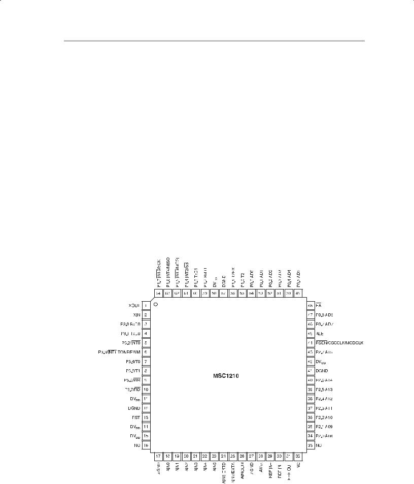
1.2 MSC1210 Pin-Out
The names and functions of these pins are similar to those found on a traditional 8052 core, but the MSC1210 includes additional pin assignments to support the additional functions specific to the part.
Figure 1−2. Pin Configuration of the MSC1210
Introduction to the MSC1210 |
1-3 |
|

MSC1210 Pin-Out
Table 1−1. Pin Descriptions of the MSC1210
Pin # |
Name |
Description |
|
|
|
|
|
|
|
|
|
|
|
|
|
|
|
|
|
1 |
XOUT |
The crystal oscillator pin XOUT supports parallel resonant AT cut crys- |
|||||||
|
|
tals and ceramic resonators. XOUT serves as the output of the crystal |
|||||||
|
|
amplifier. |
|
|
|
|
|
|
|
|
|
|
|
|
|
|
|
|
|
2 |
XIN |
The crystal oscillator pin XIN supports parallel resonant AT cut crystals |
|||||||
|
|
and ceramic resonators. XIN can also be an input if there is an external |
|||||||
|
|
clock source instead of a crystal. |
|
||||||
|
|
|
|
|
|
|
|
|
|
3-10 |
P3.0-P3.7 |
Port 3 is a bidirectional I/O port. The alternate functions for Port3 are |
|||||||
|
|
listed below. |
|
|
|
|
|
|
|
|
|
Port 3—Alternate Functions: |
|
||||||
|
|
|
|
|
|
|
|
|
|
|
|
PORT |
ALTERNATE |
|
MODE |
||||
|
|
|
|
|
|
|
|
|
|
|
|
P3.0 |
RxD0 |
|
Serial Port 0 Input |
||||
|
|
|
|
|
|
|
|
|
|
|
|
P3.1 |
TxD0 |
|
Serial Port 0 Output |
||||
|
|
|
|
|
|
|
|
|
|
|
|
P3.2 |
|
|
|
|
External Interrupt 0 |
||
|
|
|
INT0 |
|
|
||||
|
|
|
|
|
|
|
|
||
|
|
P3.3 |
|
|
|
|
|
|
External Interrupt 1/TONE/PWM Out- |
|
|
|
INT1/TONE/ |
|
|||||
|
|
|
PWM |
|
put |
||||
|
|
|
|
|
|
|
|
||
|
|
P3.4 |
T0 |
|
Timer 0 External Input |
||||
|
|
|
|
|
|
|
|
||
|
|
P3.5 |
T1 |
|
Timer 1 External Input |
||||
|
|
|
|
|
|
|
|
||
|
|
P3.6 |
|
|
|
External Data Memory Write Strobe |
|||
|
|
|
WR |
|
|
||||
|
|
|
|
|
|
|
|||
|
|
P3.7 |
|
|
External Data Memory Read Strobe |
||||
|
|
|
RD |
|
|
||||
|
|
|
|
|
|
|
|
|
|
11, 14, 15, |
DVDD |
Digital Power Supply |
|
||||||
42, 58 |
|
|
|
|
|
|
|
|
|
|
|
|
|
|
|
|
|
|
|
12, 41, 57 |
DGND |
Digital Ground |
|
|
|
|
|
|
|
|
|
|
|||||||
13 |
RST |
A HIGH on the reset input for two instruction clock cycles will reset the |
|||||||
|
|
device. |
|
|
|
|
|
|
|
|
|
|
|
|
|
|
|
|
|
16, 32, 33 |
NC |
No Connection |
|
|
|
|
|
|
|
|
|
|
|
|
|
|
|
|
|
17, 27 |
AGND |
Analog Ground |
|
|
|
|
|
|
|
|
|
|
|
||||||
28 |
AVDD |
Analog Power Supply |
|
||||||
|
|
|
|
||||||
18 |
AIN0 |
Analog Input Channel 0 |
|
||||||
|
|
|
|
||||||
19 |
AIN1 |
Analog Input Channel 1 |
|
||||||
|
|
|
|
||||||
20 |
AIN2 |
Analog Input Channel 2 |
|
||||||
|
|
|
|
||||||
21 |
AIN3 |
Analog Input Channel 3 |
|
||||||
|
|
|
|
||||||
22 |
AIN4 |
Analog Input Channel 4 |
|
||||||
|
|
|
|
||||||
23 |
AIN5 |
Analog Input Channel 5 |
|
||||||
|
|
|
|||||||
24 |
AIN6, EXTD |
Analog Input Channel 6, Digital Low Voltage Detect Input |
|||||||
|
|
|
|||||||
25 |
AIN7, EXTA |
Analog Input Channel 7, Analog Low Voltage Detect Input |
|||||||
|
|
|
|||||||
26 |
AINCOM |
Analog Common for Single−Ended Inputs |
|||||||
|
|
|
|||||||
29 |
REF IN– |
Voltage Reference Negative Input |
|||||||
|
|
|
|
||||||
30 |
REF IN+ |
Voltage Reference Positive Input |
|
||||||
|
|
|
|
||||||
31 |
REF OUT |
Voltage Reference Output |
|
||||||
|
|
|
|
|
|
|
|
|
|
1-4

|
|
|
|
|
|
|
|
|
|
MSC1210 Pin-Out |
|
Table 1−1 Pin Descriptions of the MSC1210 (Continued) |
|
|
|||||||||
|
|
|
|
|
|
|
|
|
|
|
|
Pin # |
|
Name |
Description |
|
|
|
|
|
|
|
|
|
|
|
|
|
|
|
|
|
|
|
|
34-40, 43 |
|
P2.0-P2.7 |
Port 2 is a bidirectional I/O port. The alternate functions for Port 2 are |
|
|||||||
|
|
|
|
listed below. |
|
|
|
|
|
|
|
|
|
|
|
Port 2—Alternate Functions: |
|
|
|||||
|
|
|
|
|
|
|
|
|
|
|
|
34-40, 43 |
|
P2.0-P2.7 |
PORT |
|
ALTERNATE |
MODE |
|
||||
|
|
|
|
|
|
|
|
|
|
|
|
|
|
|
|
P2.0 |
|
A8 |
Address Bit 8 |
|
|||
|
|
|
|
|
|
|
|
|
|
|
|
|
|
|
|
P2.1 |
|
A9 |
Address Bit 9 |
|
|||
|
|
|
|
|
|
|
|
|
|
|
|
|
|
|
|
P2.2 |
|
A10 |
Address Bit 10 |
|
|||
|
|
|
|
|
|
|
|
|
|
|
|
|
|
|
|
P2.3 |
|
A11 |
Address Bit 11 |
|
|||
|
|
|
|
|
|
|
|
|
|
|
|
|
|
|
|
P2.4 |
|
A12 |
Address Bit 12 |
|
|||
|
|
|
|
|
|
|
|
|
|
|
|
|
|
|
|
P2.5 |
|
A13 |
Address Bit 13 |
|
|||
|
|
|
|
|
|
|
|
|
|
|
|
|
|
|
|
P2.6 |
|
A14 |
Address Bit 14 |
|
|||
|
|
|
|
|
|
|
|
|
|
|
|
|
|
|
|
P2.7 |
|
A15 |
Address Bit 15 |
|
|||
|
|
|
|
|
|
|
|
|
|
|
|
44 |
|
PSEN, OSCCLK, |
Program Store Enable: Connected to optional external memory as a |
|
|||||||
|
|
MODCLK |
chip enable. PSEN will provide an active low pulse. In programming |
|
|||||||
|
|
|
|
mode, PSEN is used as an input along with ALE to define serial or par- |
|
||||||
|
|
|
|
allel programming mode. PSEN is held HIGH for parallel programming |
|
||||||
|
|
|
|
and tied LOW for serial programming. This pin can also be selected |
|
||||||
|
|
|
|
(when not using external program memory) to output the Oscillator |
|
||||||
|
|
|
|
clock, Modulator clock, HIGH, or LOW. |
|
||||||
|
|
|
|
|
|
|
|
|
|
|
|
|
|
|
|
ALE |
|
PSEN |
|
|
|
Program Mode Selection |
|
|
|
|
|
|
|
|
|
|
|
|
|
|
|
|
|
NC |
|
NC |
Normal Operation |
|
|||
|
|
|
|
|
|
|
|
|
|
|
|
|
|
|
|
0 |
1 |
|
|
|
Parallel Programming |
|
|
|
|
|
|
|
|
|
|
|
|
|
|
|
|
|
|
1 |
0 |
|
|
|
Serial Programming |
|
|
|
|
|
|
|
|
|
|
|
|
|
|
|
|
|
|
0 |
0 |
|
|
|
Reserved |
|
|
|
|
|
|
|
|
|
|
|
|
||
45 |
|
ALE |
Address Latch Enable: Used for latching the low byte of the address |
|
|||||||
|
|
|
|
during an access to external memory. ALE is emitted at a constant rate |
|
||||||
|
|
|
|
of 1/2 the oscillator frequency, and can be used for external timing or |
|
||||||
|
|
|
|
clocking. One ALE pulse is skipped during each access to external |
|
||||||
|
|
|
|
data memory. In programming mode, ALE is used as an input along |
|
||||||
|
|
|
|
with PSEN to define serial or parallel programming mode. ALE is held |
|
||||||
|
|
|
|
HIGH for serial programming and tied LOW for parallel programming. |
|
||||||
|
|
|
|
|
|
|
|||||
48 |
|
|
|
External Access Enable: |
|
must be externally held LOW to enable |
|
||||
|
EA |
|
EA |
|
|||||||
|
|
|
|
the device to fetch code from external program memory locations start- |
|
||||||
|
|
|
|
ing with 0000H. |
|
|
|
|
|
|
|
|
|
|
|
|
|||||||
46, 47, |
|
P0.0−P0.7 |
Port 0 is a bidirectional I/O port. The alternate functions for Port 0 are |
|
|||||||
49-54 |
|
|
|
listed below. |
|
|
|
|
|
|
|
|
|
|
|
Port 0—Alternate Functions: |
|
|
|||||
|
|
|
|
|
|
|
|
|
|||
|
|
|
|
PORT |
|
ALTERNATE |
MODE |
|
|||
|
|
|
|
|
|
|
|
|
|||
|
|
|
|
P0.0 |
|
AD0 |
Address/Data Bit 0 |
|
|||
|
|
|
|
|
|
|
|
|
|||
|
|
|
|
P0.1 |
|
AD1 |
Address/Data Bit 1 |
|
|||
|
|
|
|
|
|
|
|
|
|||
|
|
|
|
P0.2 |
|
AD2 |
Address/Data Bit 2 |
|
|||
|
|
|
|
|
|
|
|
|
|||
|
|
|
|
P0.3 |
|
AD3 |
Address/Data Bit 3 |
|
|||
|
|
|
|
|
|
|
|
|
|||
|
|
|
|
P0.4 |
|
AD4 |
Address/Data Bit 4 |
|
|||
|
|
|
|
|
|
|
|
|
|
|
|
Introduction to the MSC1210 |
1-5 |
|

MSC1210 Pin-Out
Table 1−1 Pin Descriptions of the MSC1210 (Continued)
Pin # |
Name |
Description |
|
|
|
|
|
|
|
|
|
|
|
|
|
|
|
46, 47, |
P0.0−P0.7 |
P0.5 |
AD5 |
Address/Data Bit 5 |
||||
49-54 |
|
|
|
|
|
|
|
|
|
P0.6 |
AD6 |
Address/Data Bit 6 |
|||||
|
|
|||||||
|
|
|
|
|
|
|
|
|
|
|
P0.7 |
AD7 |
Address/Data Bit 7 |
||||
|
|
|
|
|
|
|
|
|
55, 56, |
P1.0−P1.7 |
Port 1 is a bidirectional I/O port. The alternate functions for Port 1 are |
||||||
59−64 |
|
listed below. |
|
|
|
|
|
|
|
|
Port 1—Alternate Functions: |
|
|||||
|
|
|
|
|
|
|
|
|
|
|
PORT |
ALTERNATE |
MODE |
||||
|
|
|
|
|
|
|
|
|
|
|
P1.0 |
T2 |
T2 Input |
||||
|
|
|
|
|
|
|
|
|
|
|
P1.1 |
T2EX |
T2 External Input |
||||
|
|
|
|
|
|
|
|
|
|
|
P1.2 |
RxD1 |
Serial Port Input |
||||
|
|
|
|
|
|
|
|
|
|
|
P1.3 |
TxD1 |
Serial Port Output |
||||
|
|
|
|
|
|
|
|
|
|
|
P1.4 |
|
|
|
|
|
External Interrupt/Slave Select |
|
|
INT2/SS |
|
|||||
|
|
|
|
|
|
|
||
|
|
P1.5 |
|
|
|
External Interrupt/Master Out−Slave In |
||
|
|
|
INT3/MOSI |
|||||
|
|
|
|
|
||||
|
|
P1.6 |
INT4/MISO |
External Interrupt/Master In−Slave Out |
||||
|
|
|
|
|
||||
|
|
P1.7 |
|
|
|
External Interrupt/Serial Clock |
||
|
|
|
INT5/SCK |
|||||
|
|
|
|
|
|
|
|
|
1.2.1I/O Ports (P0, P1, P2, and P3)
Of the 64 pins on the MSC1210, 32 of them are dedicated to I/O lines that have a one-to-one relation with SFRs P0, P1, P2, and P3. The developer may raise and lower these lines by writing 1s or 0s to the corresponding bits in the SFRs. Likewise, the current state of these lines may be found by reading the corresponding bits of the SFRs.
All of the ports have optional pull-up resistors that are enabled when the port is in 8051 mode, as configured by the PxDDRL/H SFRs. The pull-up resistors are disabled when the port is configured in any other mode, or when accessing external memory.
1.2.1.1Port 0
Port 0 is dual-function: in some designs port 0 I/O lines are available to the developer to access external devices, while in other designs it is used to access external memory. If the circuit requires external RAM, the microcontroller will use port 0 to latch in/out the 8-bit data word, as well as the low eight bits of the address in response to a MOVX instruction, as long as the hardware configuration registers are set up correctly. Port 0 I/O lines may be used for other functions as long as external data memory is not being accessed at the same time and the hardware configuration registers are set up correctly. If the circuit requires external code memory, the microcontroller will use port 0 I/O lines to access each instruction to be executed. In this case, port 0 cannot be used for other purposes, because the state of the I/O lines are constantly being modified to access external code memory.
1-6

MSC1210 Pin-Out
1.2.1.2Port 1
Port 1 consists of eight I/O lines that may be used to interface to external parts. Port 1 is commonly used to interface to external hardware such as LCDs, keypads, and other devices. As opposed to a standard 8052 core, all I/O lines of the MSC1210 serve optional alternate functions, as described below. These lines can still be used for the developing purposes, if the functions described below are not needed.
P1.0 (T2): If T2CON.1 is set (C/T2), then timer 2 is incremented whenever there is a 1-0 transition on this line. With C/T2 set, P1.0 is the clock source for timer 2.
P1.1 (T2EX): If timer 2 is in auto-reload mode and T2CON.3 (EXEN2) is set, a 1-0 transition on this line causes timer 2 to be reloaded with the auto-reload value. This also causes the T2CON.6 (EXF2) external flag to be set, which may cause an interrupt, if so enabled.
P1.2 (RxD1): If the secondary USART is being used, P1.2 (RxD1) is the pin that receives serial data. Data received via this pin is read using the SBUF1 SFR.
P1.3 (TxD1): If the secondary USART is being used, P1.3 (TxD1) is the pin that transmits serial data. Data written to the SBUF1 SFR is sent via this pin.
P1.4 (INT2/SS): This pin has two dual functions. It may be used to trigger an external 2 interrupt when a 0-1 transition is detected on this line. It is also used as slave select in SPI applications.
P1.5 (INT3/MOSI): This pin may be used to trigger an external 3 interrupt when a 1-0 transition is detected. It is also used as Master Out/Slave In in SPI applications.
P1.6 (INT4/MISO): This pin may be used to trigger an external 4 interrupt when a 0-1 transition is detected. It is also used as Master In/Slave Out in SPI applications.
P1.7 (INT5/SCK): This pin may be used to trigger an external 5 interrupt when a 1-0 transition is detected. It is also used as serial clock in SPI applications.
Introduction to the MSC1210 |
1-7 |
|

MSC1210 Pin-Out
1.2.1.3Port 2
Like port 0, port 2 is dual-function. In some circuit designs, it is available for accessing external devices, while in others it is used to address external RAM or external code memory. When more than 256 bytes of external RAM are used, port 2 is used to output the high byte of the address that is to be accessed in a MOVX operation. Whether port 2 is used to address external memory or as general I/O lines is defined by the EGP23 bit in hardware configuration Register 1.
Note:
When the EGP23 bit of hardware configuration Register 1 is set, Port 2 assumes the value of the high byte of DPTR when using the MOVX @DPTR instruction. When using the MOVX @Rx instructions, port 2 assumes the value of the MPAGE SFR.
If the circuit requires external code memory, the microcontroller automatically uses port 2 I/O lines to access each instruction to be executed, but only if bit EGP23 of HCR1 equals one. In this case, port 2 cannot be used for other purposes because the state of the I/O lines are constantly being modified to access external code memory.
1.2.1.4Port 3
Port 3 consists entirely of dual-function I/O lines. While you can access all these lines from the software by reading/writing to the P3 SFR, each pin has a predefined function that the microcontroller handles automatically when configured to do so and/or when necessary.
P3.0 (RxD0): The primary USART/serial port uses P3.0 as the receive line. For in-circuit designs that are using the microcontroller internal serial port, this is the line into which the serial data is clocked.
Note:
When interfacing an 8052 to an RS-232 port, you cannot connect this line directly to the RS-232 pin; you must pass it through a part such as the MAX233 to obtain the correct voltage levels.
You can assign any function to this pin as long as the circuit has no need to receive data via the integrated serial port.
P3.1 (TxD0): The primary USART/serial port uses P3.1 as the transmit line. For in-circuit designs that is using the microcontroller internal serial port, this is the line used by the microcontroller to clock out all data written to the SBUF SFR.
Note:
When interfacing an 8052 to an RS-232 port, you cannot connect this line directly to the RS-232 pin; you must pass it through a part such as the MAX233 to obtain the correct voltage levels.
You can assign any function to this pin as long as the circuit has no need to transmit data via the integrated serial port.
1-8
MSC1210 Pin-Out
P3.2 (INT0): When so configured, this line is used to trigger an external 0 Interrupt. This may either be low-level triggered or may be triggered on a 1-0 transition (see Chapter 10, Interrupts, for details). You can assign any function to this pin as long as the circuit has no need to trigger an external 0 interrupt.
P3.3 (INT1/TONE/PWM): When so configured, this line is used to trigger an external 1 Interrupt. This may either be low-level triggered or may be triggered on a 1-0 transition (see Chapter 10, Interrupts, for details). This pin is also used for outputting PWM, if so configured.
P3.4 (T0): When so configured, this line is used as the clock source for timer 0. Timer 0 is incremented either every instruction cycle that T0 is high, or every time there is a 1-0 transition on this line, depending on how the timer is configured (see Chapter 8, Timers, for details). You can assign any function to this pin as long as the circuit has no need to control timer 0 externally.
P3.5 (T1): When so configured, this line is used as the clock source for timer 1. Timer 1 is incremented either every instruction cycle that T1 is high, or every time there is a 1-0 transition on this line, depending on how the timer is configured (see Chapter 8, Timers, for details). You can assign any function to this pin as long as the circuit has no need to control timer 1 externally.
P3.6 (WR): This is the external memory write strobe line when bit EGP23 is set in hardware configuration Register 1. This line is asserted low by the microcontroller whenever a MOVX instruction writes to external RAM. This line should be connected to the RAM write (W) line. You can assign any function to this pin as long as the circuit does not write to external RAM using MOVX.
P3.7 (RD): This is the external memory read strobe line when bit EGP23 is set in hardware configuration Register 1. This line is asserted low by the microcontroller whenever a MOVX instruction is read from external RAM. This line must be connected to the RAM read (R) line. You can assign any function to this pin as long as the circuit does not read from external RAM using MOVX.
1.2.2Oscillator Inputs (XTAL1 and XTAL2)
The MSC1210 is typically driven by a crystal connected to pins 1 (XOUT) and 2 (XIN). Common crystal frequencies are 11.0592MHz as well as 12MHz, although the MSC1210 is capable of accepting frequencies as high as 33MHz.
While a crystal is the normal clock source, this is not always the case. A digital clock source may also be attached to XIN and XOUT to provide the clock for the microcontroller.
Introduction to the MSC1210 |
1-9 |
|

MSC1210 Pin-Out
1.2.3Reset Line (RST)
Pin 13 is the master reset line for the microcontroller. When this pin is brought high for two instruction cycles, the microcontroller is effectively reset. SFRs, including the I/O ports, are restored to their default conditions and the program counter is reset to 0000H. Keep in mind that Internal RAM is not affected by a reset. The microcontroller begins executing code at 0000H when pin 13 returns to a low state.
The reset line is often connected to a reset button/switch that you can press to reset the circuit. It is also common to connect the reset line to a watchdog IC or a supervisor IC (such as MAX707). Traditional resistor-capacitor networks attached to the reset line also work well because the RST input is a Schmitt trigger input.
1.2.4Address Latch Enable (ALE)
The ALE at pin 45 is an output-only pin that is controlled entirely by the microcontroller and allows the microcontroller to multiplex the low-byte of a memory address and the 8-bit data itself on port 0. This is because, while the high byte of the memory address is sent on port 2, port 0 is used both to send the low byte of the memory address and the data itself. This is accomplished by placing the low byte of the address on port 0, exerting an ALE high-to-low transition to latch the low byte of the address into a latch IC (such as the 74HC573), and then placing the 8 data bits on port 0. In this way, the MSC1210 is able to output a 16-bit address and an 8-bit data word with 16 I/O lines instead of 24.
The ALE line is used in this fashion both to access external RAM with MOVX @DPTR, as well as to accessi instructions in external code memory. When the program is executed from external code memory, ALE pulses at a rate that is ¼ that of the oscillator frequency. Thus, if the oscillator operates at 11.0592MHz, ALE pulses at a rate of 2 764 800 times per second. When the MOVX instruction is executed, one PSEN pulse is missed in lieu of a pulse on WR or RD.
This pin is also used when programming the part, along with PSEN, as an input during reset to indicate whether programming will occur in serial or parallel mode. If this line is held high when in programming mode, programming will occur in serial mode.
1.2.5Program Store Enable (PSEN)
The program store enable (PSEN) line at pin 44 is exerted low automatically by the microcontroller whenever it accesses external code memory. This line should be attached to the output enable (OE) pin of the device that contains your code memory. The PSEN signal is applied for both internal and external memory access.
This pin is also used when programming the part, along with ALE, as an input to indicate whether programming will occur in serial or parallel mode. If this line is held high when in programming mode, programming will occur in parallel mode.
1-10

MSC1210 Pin-Out
1.2.6External Access (EA)
The external access (EA) line at pin 48 is used to determine whether the MSC1210 will execute your program from external code memory or from internal code memory. If EA is tied high (connected to supply), the microcontroller will execute the program it finds in internal/on-chip code memory. If EA is tied low (to ground), it will attempt to execute the program that it finds in the attached external program memory. Of course, the external program memory must be properly connected for the microcontroller to be able to access the program in external program memory.
The EA pin is ignored during serial or parallel flash programming modes.
Note:
Even when EA is tied high (indicating that the microcontroller should execute from internal code memory), the microcontroller will attempt to execute from external code memory if the program counter references an address not available for the chip you are using, or if you are accessing program memory in excess of the amount of flash memory that you have partitioned for program memory. For example, if you have partitioned 4k of flash memory to be program memory and you tie EA high, the derivative starts executing the program it finds on-chip. However, if your on-chip program attempts to execute code above 0FFFH (that is, exceeding 4k), then the MSC1210 will attempt to execute that code at that address from external code memory. Thus, it is possible to have a split design, in which some of the code is found on-chip and the rest is found off-chip.
Introduction to the MSC1210 |
1-11 |
|
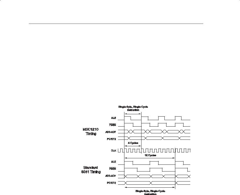
Enhanced 8051 Core
1.3 Enhanced 8051 Core
The MSC1210 is an 8052-based family of high-performance, mixed-signal controllers. All instructions in the MSC1210 family perform exactly the same function as they would in a standard 8052 core. Although the effect on bits, flags, and registers is the same, the timing is different.
The MSC1210 family uses an efficient 8052 core that results in an improved instruction execution speed of three times faster than the original core for the same external clock speed (4 clock cycles per instruction versus 12 clock cycles per instruction, as shown in Figure 1−3). This allows you to run the device at slower external clock speeds, which reduces system noise and power consumption, but provides greater throughput.
Figure 1−3. MSC1210 Timing Compared to Standard 8051 Timing
The timing of software loops is faster with the MSC1210 than with the standard 8052. However, the timer/counter operation of the MSC1210 may be maintained at 12 clocks per increment or optionally run at 4 clocks per increment.
You can develop software for the MSC1210 with the existing 8052 development tools because the MSC1210 is fully compatible with the standard 8052 instruction set. Additionally, a complete integrated development environment is provided with each demonstration board.
1-12

Family Device Compatibility
1.4 Family Device Compatibility
The hardware functionality and pin outs across the MSC1210 family are fully compatible. The only difference between family members is the memory configuration and this enables simple migration between family members. Code written for the 4K bytes program memory version of the MSC1210 can be executed directly on the 8K, 16K, or 32K versions. This allows you to add or delete software functions and to freely migrate between family members.
The MSC1210 can become a standard device used across several application platforms.
1.5 Flash Memory
The MSC1210 features flexible flash memory that allows you to uniquely configure the program and non-volatile data memory maps to meet the needs of the application. The flash memory is programmable over the entire operating voltage range and temperature range using both serial and parallel programming methods.
1.6 High Performance Analog Functions
The analog functionality is state-of-the-art. The ADC is extremely low noise, which enables you to meet even the most stringent analog requirements. The integrated programmable gain amplifier (PGA) further improves the performance of the ADC. This effectively provides for resolution into the nanovolt range.
The on-chip voltage reference provides for low drift and high accuracy, thus eliminating the need for an external voltage reference.
These features are integrated with other analog functions, such as a programmable filter, multiplexer, temperature sensor, burnout current sources, analog input buffer, and an offset correction digital-to-analog converter (DAC).
Introduction to the MSC1210 |
1-13 |
|

High-Performance Peripherals
1.7 High-Performance Peripherals
High-performance peripherals are included on-chip, which offload CPU processing and control functions from the core to further improve the overall device efficiency and throughput. On-chip peripherals include additional SRAM, a 32-bit accumulator, an SPI-compatible serial port with a FIFO buffer, dual USARTs, on-chip power-on reset, brownout reset, low-voltage detect, multiple digital ports with configurable I/O, a 16-bit pulse width modulator (PWM), a watchdog timer, and three timer/counters.
For instance, the SPI interface uses a FIFO buffer, which allows for the serial transmission and reception of data with virtually no CPU overhead. The FIFO buffer function allows for the transfer of large amounts of data at faster transfer rates than more conventional methods.
Additionally, the 32-bit accumulator significantly reduces the processing overhead for the multiple byte data from the ADC or other sources. This allows for 24-bit addition, subtraction, and shifting to be accomplished without using CPU resources. This can reduce both the code size and code execution time.
1-14

Chapter 2
MSC1210 Memory Organization
This chapter defines the Memory Organization of MSC1210 ADC.
Topic |
|
Page |
|
|
|
2.1 |
Description . . . . . . . . . . . . . . . . . . . . . . . . . . . . . . . . . . . . . . . . . . . . . . . . . |
. . 2-2 |
2.2 |
Program Memory . . . . . . . . . . . . . . . . . . . . . . . . . . . . . . . . . . . . . . . . . . . |
. . 2-2 |
2.3 |
Data Memory . . . . . . . . . . . . . . . . . . . . . . . . . . . . . . . . . . . . . . . . . . . . . . . . |
. 2-4 |
2.4 |
Internal RAM . . . . . . . . . . . . . . . . . . . . . . . . . . . . . . . . . . . . . . . . . . . . . . . . |
. 2-6 |
|
|
|
MSC1210 Memory Organization |
2-1 |
|
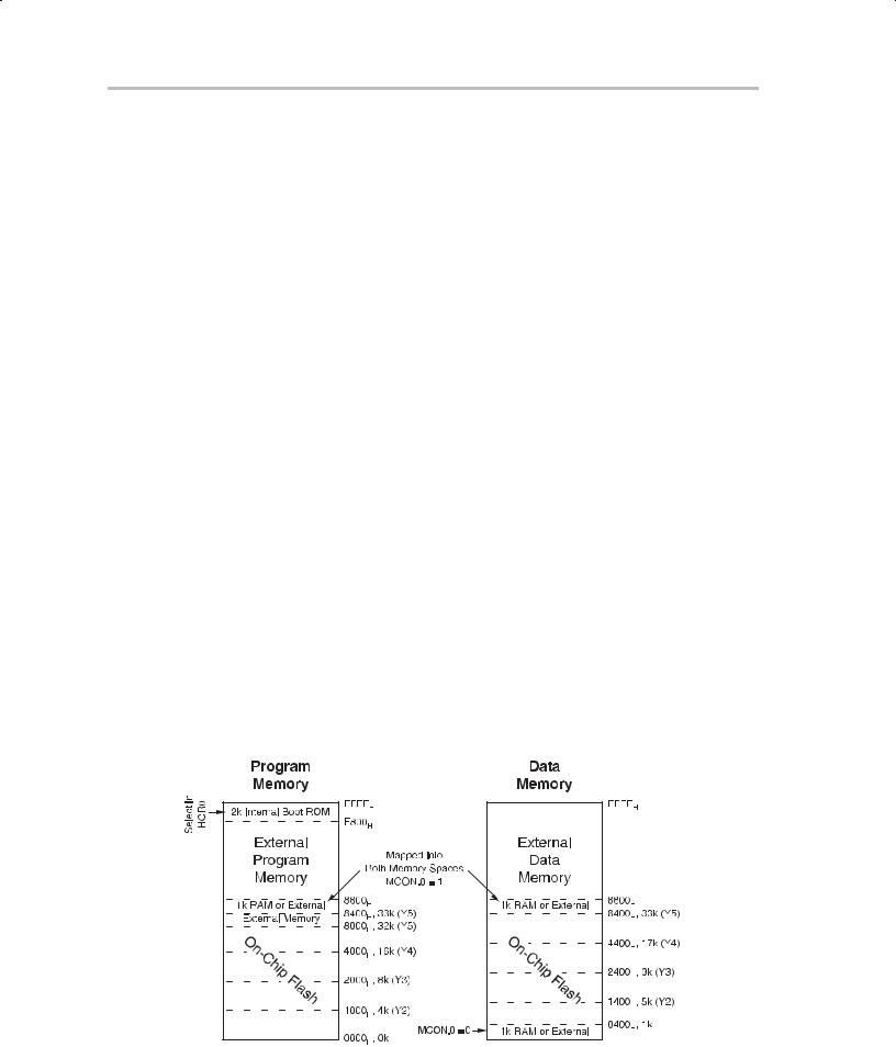
Description
2.1 Description
The MCS1210 has three very general types of memory. To program the MCS1210 effectively, it is necessary to have a basic understanding of these memory types:
-Special Function Registers refer to 128 bytes that control the operation of the MSC1210.
-Program Memory is used to store the actual program that may reside onchip, off-chip, or both.
-Data Memory is static random access memory (SRAM) that can reside on-chip, off-chip, or both. The MSC1210 has four types of data memory:
J On-chip extended SRAM
J Off-chip external SRAM
J On-chip Flash Data memory
J Internal RAM
2.2Program Memory
Program memory holds the actual program that is to be run. This memory includes the on-chip flash memory designated as program memory and/or external memory.
The MSC1210 family offers a maximum of 32k of on-chip flash program memory. The exact amount of on-chip program memory depends on the specific MSC1210 version selected and how the flash memory of that chip has been partitioned between program and data memory. Figure 2−1 illustrates how the flash memory may be distributed between these two types of memory.
Figure 2−1. MSC1210 Memory Map
2-2

Program Memory
For example, in the Y5 model there is 32k flash memory available. This 32k may be configured as either program memory, data memory, or both. This configuration is set at the moment the firmware is loaded onto the MSC1210 by setting hardware configuration register HCR0 as per Table 2−1. This table indicates the total amount of program and data memory available for each part revision given a specific HCR0 setting.
Table 2−1. Program and Data Memory Size.
HCR0 |
MSC1210Y2 |
MSC1210Y3 |
MSC1210Y4 |
MSC1210Y5 |
||||
|
|
|
|
|
|
|
|
|
DFSEL |
PM |
DM |
PM |
DM |
PM |
DM |
PM |
DM |
|
|
|
|
|
|
|
|
|
000 |
0kB |
4kB |
0kB |
8kB |
0kB |
16kB |
0kB |
32kB |
|
|
|
|
|
|
|
|
|
001 |
0kB |
4kB |
0kB |
8kB |
0kB |
16kB |
0kB |
32kB |
|
|
|
|
|
|
|
|
|
010 |
0kB |
4kB |
0kB |
8kB |
0kB |
16kB |
16kB |
16kB |
|
|
|
|
|
|
|
|
|
011 |
0kB |
4kB |
0kB |
8kB |
8kB |
8kB |
24kB |
8kB |
|
|
|
|
|
|
|
|
|
100 |
0kB |
4kB |
4kB |
4kB |
12kB |
4kB |
28kB |
4kB |
|
|
|
|
|
|
|
|
|
101 |
2kB |
2kB |
6kB |
2kB |
14kB |
2kB |
30kB |
2kB |
|
|
|
|
|
|
|
|
|
110 |
3kB |
1kB |
7kB |
1kB |
15kB |
1kB |
31kB |
1kB |
|
|
|
|
|
|
|
|
|
111 (default) |
4kB |
0kB |
8kB |
0kB |
16kB |
0kB |
32kB |
0kB |
|
|
|
|
|
|
|
|
|
Note: When a 0kB program memory configuration is selected, program execution is external
For example, setting the DFSEL bits to 110 with a MSC1210Y5 would cause 31kb of on-chip flash memory to be partitioned as program memory and 1kb of flash memory to be partitioned as data memory.
Table 2−2 indicates where the assigned memory will be located in address space. This table provides essentially the same information as Table 2−1, but also indicates where the memory will be located. For example, the DFSEL = 110 example in the previous paragraph (31kb of on-chip flash program memory, 1k of on-chip flash data memory) appears in Table 2−2 as flash program memory from 0000H to 7BFFH (which is 31k) and flash data memory from 0400H to 07FFH (which is 1k).
Note that the Data memory address starts at 0400H because the first 1k (0000H-03FFH) is, by default, used to address the on-chip extended SRAM. The location of on-chip extended SRAM may be changed by using the Memory Control (MCON) SFR. By setting bit 0 of MCON, the on-chip extended SRAM may be moved from 0000H-03FFH to 8400H-87FFH. However, on-chip extended flash data memory always begins at 0400H regardless of whether or not SRAM is located at 0000H or 8400H.
MSC1210 Memory Organization |
2-3 |
|

Data Memory
Table 2−2. Program and Data Memory Addresses.
HCR0 |
MSC1210Y2 |
MSC1210Y3 |
MSC1210Y4 |
MSC1210Y5 |
||||
|
|
|
|
|
|
|
|
|
DFSEL |
PM |
DM |
PM |
DM |
PM |
DM |
PM |
DM |
|
|
|
|
|
|
|
|
|
000 (reserved) |
— |
— |
— |
— |
— |
— |
— |
— |
|
|
|
|
|
|
|
|
|
001 |
— |
— |
— |
— |
— |
— |
0000 |
0400-83FF |
|
|
|
|
|
|
|
|
|
010 |
— |
— |
— |
— |
0000 |
0400-43FF |
0000-3FFF |
0400-43FF |
|
|
|
|
|
|
|
|
|
011 |
— |
— |
0000 |
0400-23FF |
0000-1FFF |
0400-23FF |
0000-5FFF |
0400-23FF |
|
|
|
|
|
|
|
|
|
100 |
0000 |
0400-13FF |
0000-0FFF |
0400-13FF |
0000-2FFF |
0400-13FF |
0000-6FFF |
0400-13FF |
|
|
|
|
|
|
|
|
|
101 |
0000-07FF |
0400-00BF |
0000-17FF |
0400-0BFF |
0000-37FF |
0400-0BFF |
0000-77FF |
0400-0BFF |
|
|
|
|
|
|
|
|
|
110 |
0000-00BF |
0400-07FF |
0000-1BFF |
0400-07FF |
0000-3BFF |
0400-07FF |
0000-7BFF |
0400-07FF |
|
|
|
|
|
|
|
|
|
111 (default) |
0000-0FFF |
0000 |
0000-1FFF |
0000 |
0000-3FFF |
0000 |
0000-7FFF |
0000 |
|
|
|
|
|
|
|
|
|
Note: Program accesses above the highest listed address will access external Program memory.
Program memory addressing beyond the on-chip address range is accessed externally via ports 0 and 2. The total amount of code memory, on-chip and off, is limited to 64k due to limitations of the 8052 architecture.
Note:
MSC1210 programs are limited to 64k because code memory is restricted to 64k. Some compilers offer ways to get around this limit when used with specially wired hardware. However, without such special compilers and hardware, programs are limited to 64k.
The MSC1210 includes 2k of boot ROM code that controls operation during serial or parallel programming. In program mode, the boot ROM is located in the first 2kB of program memory.
The boot ROM is available to your program as long as EBR (hardware configuration register 0, bit 4) is set, which is the default. When enabled, the boot ROM routines will be located at program memory addresses F800H-FFFFH. The boot ROM includes a number of functions such as flash memory access, and serial routines including data transmission, reception, and auto-baud.
2.3 Data Memory
Data memory is divided into four types of memory, depending on its location and volatility: internal RAM, on-chip extended SRAM, off-chip external SRAM, and on-chip flash data memory. However, data memory (regardless of its location or volatility) is accessed using the MOVX instruction, except for internal RAM, which is accessed using the MOV instruction.
2.3.1On-Chip Extended Static RAM (SRAM)
The MSC1210 includes 1024 bytes of on-chip extended static RAM (SRAM). Even though this memory resides on-chip, it is accessed using the MOVX instruction as if it were external data memory. Whenever a program accesses data memory addresses 0000H through 03FFH, the on-chip external SRAM is used.
2-4
 Loading...