


Philips 74HCT03PW, 74HCT03N, 74HCT03DB, 74HCT03D, 74HC03PW Datasheet
...
INTEGRATED CIRCUITS
DATA SHEET
For a complete data sheet, please also download:
∙The IC06 74HC/HCT/HCU/HCMOS Logic Family Specifications
∙The IC06 74HC/HCT/HCU/HCMOS Logic Package Information
∙The IC06 74HC/HCT/HCU/HCMOS Logic Package Outlines
74HC/HCT03
Quad 2-input NAND gate
Product specification |
|
December 1990 |
|||||
File under Integrated Circuits, IC06 |
|
|
|
|
|
|
|
|
|
|
|
|
|
|
|
|
|
|
|
|
|
|
|
|
|
|
|
|
|
|
|

Philips Semiconductors |
Product specification |
|
|
|
|
Quad 2-input NAND gate |
74HC/HCT03 |
|
|
|
|
FEATURES
·Level shift capability
·Output capability: standard (open drain)
·ICC category: SSI
GENERAL DESCRIPTION
The 74HC/HCT03 are high-speed Si-gate CMOS devices and are pin compatible with low power Schottky TTL (LSTTL). They are specified in compliance with JEDEC standard no. 7A.
QUICK REFERENCE DATA
GND = 0 V; Tamb = 25 °C; tr = tf = 6 ns
The 74HC/HCT03 provide the 2-input NAND function.
The 74HC/HCT03 have open-drain N-transistor outputs, which are not clamped by a diode connected to VCC. In the OFF-state, i.e. when one input is LOW, the output
may be pulled to any voltage between GND and VOmax. This allows the device to be used as a LOW-to-HIGH or
HIGH-to-LOW level shifter. For digital operation and OR-tied output applications, these devices must have a pull-up resistor to establish a logic HIGH level.
SYMBOL |
PARAMETER |
CONDITIONS |
TYPICAL |
UNIT |
||
|
|
|||||
HC |
HCT |
|||||
|
|
|
|
|||
|
|
|
|
|
|
|
tPZL/ tPLZ |
propagation delay |
CL = 15 pF; RL = 1 kW; VCC = 5 V |
8 |
10 |
ns |
|
CI |
input capacitance |
|
3.5 |
3.5 |
pF |
|
CPD |
power dissipation capacitance per gate |
notes 1, 2 and 3 |
4.0 |
4.0 |
pF |
|
Notes
1. CPD is used to determine the dynamic power dissipation (PD in mW):
PD = CPD ´ VCC2´ fi + å (CL ´ VCC2 ´ fo) + å (VO2/RL) ´ duty factor LOW, where:
fi = input frequency in MHz fo = output frequency in MHz VO = output voltage in V
CL = output load capacitance in pF VCC = supply voltage in V
RL = pull-up resistor in MW
å(CL ´ VCC2 ´ fo) = sum of outputs
å(VO2/RL) = sum of outputs
2.For HC the condition is VI = GND to VCC
For HCT the condition is VI = GND to VCC - 1.5 V
3.The given value of CPD is obtained with: CL = 0 pF and RL = ¥
ORDERING INFORMATION
See “74HC/HCT/HCU/HCMOS Logic Package Information”.
December 1990 |
2 |
Philips Semiconductors |
|
Product specification |
|
|
|
Quad 2-input NAND gate |
74HC/HCT03 |
|
|
|
|
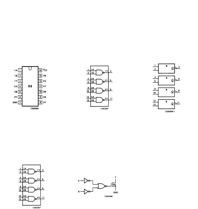
PIN DESCRIPTION |
|
|
|
|
|
PIN NO. |
SYMBOL |
NAME AND FUNCTION |
|
|
|
1, 4, 9, 12 |
1A to 4A |
data inputs |
2, 5, 10, 13 |
1B to 4B |
data inputs |
3, 6, 8, 11 |
1Y to 4Y |
data outputs |
7 |
GND |
ground (0 V) |
14 |
VCC |
positive supply voltage |
Fig.1 |
Pin configuration. |
|
Fig.2 Logic symbol. |
|
|
Fig.3 IEC logic symbol. |
|||
|
|
|
|
|
|
|
|
|
|
|
|
|
|
|
FUNCTION TABLE |
||||
|
|
|
|
|
|||||
|
|
|
|
|
|
|
|
|
|
|
|
|
|
|
INPUTS |
OUTPUT |
|
||
|
|
|
|
|
|
|
|
|
|
|
|
|
|
|
nA |
|
nB |
nY |
|
|
|
|
|
|
|
|
|
|
|
|
|
|
|
|
L |
|
L |
Z |
|
|
|
|
|
|
L |
|
H |
Z |
|
|
|
|
|
|
H |
|
L |
Z |
|
|
|
|
|
|
H |
|
H |
L |
|
|
|
|
|
|
|
|
|
|
|
|
|
|
|
|
Note |
|
|
|
|
|
|
|
|
|
1. H = HIGH voltage level |
||||
|
|
|
|
|
L = LOW voltage level |
||||
|
|
|
|
|
Z = high impedance OFF-state |
||||
Fig.4 |
Functional diagram. |
|
Fig.5 Logic diagram (one gate). |
|
|
|
|
|
|
|
|
|
|
|
|
|
|
|
|
December 1990 |
3 |
|
|
|
|
|
|
||
 Loading...