


Philips 74HCT173U, 74HCT173NB, 74HCT173N, 74HCT173DB, 74HCT173D Datasheet
...
INTEGRATED CIRCUITS
DATA SHEET
For a complete data sheet, please also download:
∙The IC06 74HC/HCT/HCU/HCMOS Logic Family Specifications
∙The IC06 74HC/HCT/HCU/HCMOS Logic Package Information
∙The IC06 74HC/HCT/HCU/HCMOS Logic Package Outlines
74HC/HCT173
Quad D-type flip-flop; positive-edge trigger; 3-state
Product specification |
|
December 1990 |
|||||
File under Integrated Circuits, IC06 |
|
|
|
|
|
|
|
|
|
|
|
|
|
|
|
|
|
|
|
|
|
|
|
|
|
|
|
|
|
|
|

Philips Semiconductors |
Product specification |
|
|
|
|
Quad D-type flip-flop; positive-edge trigger; 3-state |
74HC/HCT173 |
|
|
|
|
FEATURES
·Gated input enable for hold (do nothing) mode
·Gated output enable control
·Edge-triggered D-type register
·Asynchronous master reset
·Output capability: bus driver
·ICC category: MSI
GENERAL DESCRIPTION
The 74HC/HCT173 are high-speed Si-gate CMOS devices and are pin compatible with low power Schottky TTL (LSTTL). They are specified in compliance with JEDEC standard no. 7A.
The 74HC/HCT173 are 4-bit parallel load registers with clock enable control, 3-state buffered outputs (Q0 to Q3) and master reset (MR).
When the two data enable inputs (E1 and E2) are LOW, the data on the Dn inputs is loaded into the register
QUICK REFERENCE DATA
GND = 0 V; Tamb = 25 °C; tr = tf = 6 ns
synchronously with the LOW-to-HIGH clock (CP) transition. When one or both En inputs are HIGH one set-up time prior to the LOW-to-HIGH clock transition, the register will retain the previous data. Data inputs and clock enable inputs are fully edge-triggered and must be stable only one set-up time prior to the LOW-to-HIGH clock transition.
The master reset input (MR) is an active HIGH asynchronous input. When MR is HIGH, all four flip-flops are reset (cleared) independently of any other input condition.
The 3-state output buffers are controlled by a 2-input NOR gate. When both output enable inputs (OE1 and OE2) are LOW, the data in the register is presented to the Qn
outputs. When one or both OEn inputs are HIGH, the outputs are forced to a high impedance OFF-state. The 3-state output buffers are completely independent of the register operation; the OEn transition does not affect the clock and reset operations.
SYMBOL |
PARAMETER |
CONDITIONS |
TYPICAL |
UNIT |
||
|
|
|||||
HC |
HCT |
|||||
|
|
|
|
|||
|
|
|
|
|
|
|
tPHL/ tPLH |
propagation delay |
CL = 15 pF; VCC = 5 V |
|
|
|
|
|
CP to Qn |
|
17 |
17 |
ns |
|
|
MR to Qn |
|
13 |
17 |
ns |
|
fmax |
maximum clock frequency |
|
88 |
88 |
MHz |
|
CI |
input capacitance |
|
3.5 |
3.5 |
pF |
|
CPD |
power dissipation |
notes 1 and 2 |
20 |
20 |
pF |
|
|
capacitance per flip-flop |
|
|
|
|
|
|
|
|
|
|
|
|
Notes |
|
|
|
|
|
|
1. CPD is used to determine the dynamic power dissipation (PD in mW): |
|
|
|
|||
PD = CPD ´ VCC2 ´ fi + å (CL ´ VCC2 ´ fo) where: |
|
|
|
|||
fi = input frequency in MHz |
|
|
|
|
||
fo = output frequency in MHz |
|
|
|
|
||
å (CL ´ VCC2 |
´ fo) = sum of outputs |
|
|
|
|
|
CL = output load capacitance in pF
VCC = supply voltage in V
2.For HC the condition is VI = GND to VCC
For HCT the condition is VI = GND to VCC -1.5 V
ORDERING INFORMATION
See “74HC/HCT/HCU/HCMOS Logic Package Information”.
December 1990 |
2 |
Philips Semiconductors |
|
Product specification |
||||||||
|
|
|
|
|
|
|
|
|
|
|
Quad D-type flip-flop; positive-edge trigger; 3-state |
74HC/HCT173 |
|||||||||
|
|
|
|
|
|
|
|
|
|
|
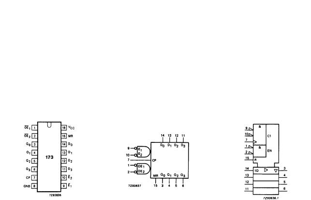
PIN DESCRIPTION |
|
|
||||||||
|
|
|
|
|
||||||
PIN NO. |
|
SYMBOL |
NAME AND FUNCTION |
|
||||||
|
|
|
|
|
|
|
|
|
|
|
1, 2 |
|
|
|
1, |
|
|
2 |
output enable input (active LOW) |
|
|
|
OE |
|
OE |
|
||||||
3, 4, 5, 6 |
|
Q0 to Q3 |
3-state flip-flop outputs |
|
||||||
7 |
|
CP |
clock input (LOW-to-HIGH, edge-triggered) |
|
||||||
8 |
|
GND |
ground (0 V) |
|
||||||
9, 10 |
|
|
|
2 |
data enable inputs (active LOW) |
|
||||
|
E |
1, |
E |
|
||||||
14, 13, 12, 11 |
|
D0 to D3 |
data inputs |
|
||||||
15 |
|
MR |
asynchronous master reset (active HIGH) |
|
||||||
16 |
|
VCC |
positive supply voltage |
|
||||||
Fig.1 Pin configuration. |
|
Fig.2 Logic symbol. |
|
Fig.3 IEC logic symbol. |
|
|
|
|
|
December 1990 |
3 |
 Loading...