


74HCT4066U
Philips 74HCT4066U, 74HCT4066PW, 74HCT4066NB, 74HCT4066N, 74HCT4066DB Datasheet
...
DATA SH EET
Product specification
Supersedes data of 1998 Oct 02
File under Integrated Circuits, IC06
1998 Nov 10
INTEGRATED CIRCUITS
74HC/HCT4066
Quad bilateral switches
For a complete data sheet, please also download:
•The IC06 74HC/HCT/HCU/HCMOS Logic Family Specifications

1998 Nov 10 2
Philips Semiconductors Product specification
Quad bilateral switches 74HC/HCT4066
FEATURES
• Very low “ON” resistance:
50 Ω (typ.) at VCC= 4.5 V
45 Ω (typ.) at VCC= 6.0 V
35 Ω (typ.) at VCC= 9.0 V
• Output capability: non-standard
• ICC category: SSI.
GENERAL DESCRIPTION
The 74HC/HCT4066 are high-speed Si-gate CMOS
devices and are pin compatible with the “4066” of the
“4000B” series. They are specified in compliance with
JEDEC standard no. 7A.
The 74HC/HCT4066 have four independent analog
switches. Each switch has two input/output terminals (nY,
nZ) and an active HIGH enable input (nE). When nE is
LOW the belonging analog switch is turned off.
The “4066” is pin compatible with the “4016” but exhibits a
much lower “ON” resistance. In addition, the “ON”
resistance is relatively constant over the full input signal
range.
QUICK REFERENCE DATA
GND = 0 V; T
amb
=25°C; tr=tf=6ns
Notes
1. C
PD
is used to determine the dynamic power dissipation (PD in µW):
a) PD=CPD× V
CC
2
× fi+∑{(CL+ CS)×V
CC
2
× fo} where:
b) fi= input frequency in MHz
c) fo= output frequency in MHz
d) ∑ {(CL+ CS)×V
CC
2
× fo} = sum of outputs
e) CL= output load capacitance in pF
f) CS= maximum switch capacitance in pF
g) VCC= supply voltage in V
2. For HC the condition is VI= GND to V
CC
For HCT the condition is VI= GND to VCC− 1.5 V
SYMBOL PARAMETER CONDITIONS
TYPICAL
UNIT
HC HCT
t
PZH
/ t
PZL
turn-on time nE to V
os
CL= 15 pF; RL=1kΩ; VCC= 5 V 11 12 ns
t
PHZ
/ t
PLZ
turn-off time nE to V
os
13 16 ns
C
I
input capacitance 3.5 3.5 pF
C
PD
power dissipation capacitance per switch notes 1 and 2 11 12 pF
C
S
max. switch capacitance 8 8 pF
1998 Nov 10 3
Philips Semiconductors Product specification
Quad bilateral switches 74HC/HCT4066
ORDERING INFORMATION
PIN DESCRIPTION
TYPE
NUMBER
PACKAGE
NAME DESCRIPTION VERSION
74HC4066 DIP14 plastic dual in-line package; 14 leads (300 mil) SOT27-1
74HC4066 SO14 plastic small outline package; 14 leads; body width 3.9 mm SOT108-1
74HC4066 SSOP14 plastic shrink small outline package; 14 leads; body width 5.3 mm SOT337-1
74HC4066 TSSOP14 plastic thin shrink small outline package; 14 leads; body width 4.4 mm SOT402-1
74HCT4066 DIP14 plastic dual in-line package; 14 leads (300 mil) SOT27-1
74HCT4066 SO14 plastic small outline package; 14 leads; body width 3.9 mm SOT108-1
74HCT4066 SSOP14 plastic shrink small outline package; 14 leads; body width 5.3 mm SOT337-1
74HCT4066 TSSOP14 plastic thin shrink small outline package; 14 leads; body width 4.4 mm SOT402-1
PIN NO. SYMBOL NAME AND FUNCTION
1, 4, 8, 11 1Y to 4Y independent inputs/outputs
2, 3, 9, 10 1Z to 4Z independent inputs/outputs
7 GND ground (0 V)
13, 5, 6, 12 1E to 4E enable inputs (active HIGH)
14 V
CC
positive supply voltage
Fig.1 Pin configuration.
handbook, halfpage
MGR253
4066
1
2
3
4
5
6
7
8
14
13
12
11
10
9
1Y
1Z
2Z
2Y
2E
3E
GND
3Y
3Z
4Z
4Y
4E
1E
V
CC
Fig.2 Logic symbol.
handbook, halfpage
MGR254
13
11Y
21Z
42Y
32Z
83Y
93Z
114Y
104Z
1E
52E
63E
12 4E

1998 Nov 10 4
Philips Semiconductors Product specification
Quad bilateral switches 74HC/HCT4066
handbook, halfpage
MGR255
13 #
5#
6#
12 #
1
2
4
3
8
9
11
10
handbook, halfpage
MGR256
13 #
5#
6#
12 #
1
11
X1
11
X1
11
X1
11
X1
2
4
3
8
9
11
10
Fig.3 IEC logic symbol.
a. b.
Fig.4 Functional diagram.
handbook, halfpage
MGR257
11
4Y
12
4E
4Z
10
3Z
9
2Z
3
1Z
2
8
3Y
6
3E
4
2Y
5
2E
1
1Y
13
1E
FUNCTION TABLE
Note
1. H = HIGH voltage level; L = LOW voltage level.
INPUT NE SWITCH
Loff
Hon
Fig.5 Schematic diagram (one switch).
handbook, halfpage
MGR258
V
CC
GND
nE
nZ
nY
V
CC

1998 Nov 10 5
Philips Semiconductors Product specification
Quad bilateral switches 74HC/HCT4066
RATINGS
Limiting values in accordance with the Absolute Maximum System (IEC 134) Voltages are referenced to GND
(GND=0V)
Note
1. To avoid drawing V
CC
current out of terminal nZ, when switch current flows in terminal nY, the voltage drop across
the bidirectional switch must not exceed 0.4 V. If the switch current flows into terminal nZ, no VCCcurrent will flow
out of terminal nY. In this case there is no limit for the voltage drop across the switch, but the voltages at nY and nZ
may not exceed VCCor GND.
RECOMMENDED OPERATING CONDITIONS
SYMBOL PARAMETER MIN. MAX. UNIT CONDITIONS
V
CC
DC supply voltage −0.5 +11.0 V
±I
IK
DC digital input diode current 20 mA for VI<−0.5 V or VI> VCC+ 0.5 V
±I
SK
DC switch diode current 20 mA for VS<−0.5 V or VS> VCC+ 0.5 V
±I
IS
DC switch current 25 mA for −0.5 V < VS< VCC+ 0.5 V
±I
CC;
±I
GND
DC VCCor GND current 50 mA
T
stg
storage temperature range −65 +150 °C
P
tot
power dissipation per package for temperature range: −40 to +125 °C
74HC/HCT
plastic DIL 750 mW above +70 °C: derate linearly with 12 mW/K
plastic mini-pack (SO) 500 mW above +70 °C: derate linearly with 8 mW/K
P
S
power dissipation per switch 100 mW
SYMBOL PARAMETER
74HC 74HCT
UNIT CONDITIONS
min. typ. max. min. typ. max.
V
CC
DC supply voltage 2.0 5.0 10.0 4.5 5.0 5.5 V
V
I
DC input voltage range GND V
CC
GND V
CC
V
V
S
DC switch voltage range GND V
CC
GND V
CC
V
T
amb
operating ambient
temperature range
−40 +85 −40 +85 °C see DC and AC
CHARACTERISTICS
T
amb
operating ambient
temperature range
−40 +125 −40 +125 °C
t
r,tf
input rise and fall times 6.0 1000 6.0 500 ns VCC= 2.0 V
500 V
CC
= 4.5 V
400 V
CC
= 6.0 V
250 V
CC
= 10.0 V
1998 Nov 10 6
Philips Semiconductors Product specification
Quad bilateral switches 74HC/HCT4066
DC CHARACTERISTICS FOR 74HC/HCT
For 74HC: V
CC
= 2.0, 4.5, 6.0 and 9.0 V; For 74HCT: VCC= 4.5 V
Note
1. At supply voltages approaching 2 V, the analog switch ON-resistance becomes extremely non-linear. Therefore it is
recommended that these devices be used to transmit digital signals only, when using these supply voltages.
SYMBOL PARAMETER
T
amb
(°C)
UNIT
TEST CONDITIONS
74HC/HCT
V
CC
(V)
I
S
(µA)
V
IS
V
I
+25 −40 to +85 −40 to +125
min. typ. max. min. max. min. max.
R
ON
ON-resistance (peak) −− − − Ω 2.0 100 V
CC
to
GND
V
IH
or
V
IL
54 95 118 142 Ω 4.5 1000
42 84 105 126 Ω 6.0 1000
32 70 88 105 Ω 9.0 1000
R
ON
ON-resistance (rail) 80 −−−Ω2.0 100 GND V
IH
or
V
IL
35 75 95 115 Ω 4.5 1000
27 65 82 100 Ω 6.0 1000
20 55 70 85 Ω 9.0 1000
R
ON
ON-resistance (rail) 100 −−−Ω2.0 100 V
CCVIH
or
V
IL
42 80 106 128 Ω 4.5 1000
35 75 94 113 Ω 6.0 1000
27 60 78 95 Ω 9.0 1000
∆R
ON
maximum variation of
ON-resistance between
any two channels
−Ω2.0 V
CC
to
GND
V
IH
or
V
IL
5 Ω 4.5
4 Ω 6.0
3 Ω 9.0
1998 Nov 10 7
Philips Semiconductors Product specification
Quad bilateral switches 74HC/HCT4066
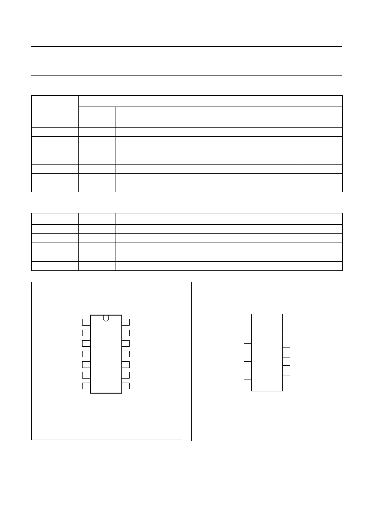
Fig.6 Test circuit for measuring ON-resistance (RON).
book, full pagewidth
MGR259
V
nY
nZ
I
is
V
is
= 0 to VCC − GND
HIGH
(from enable inputs)
GND
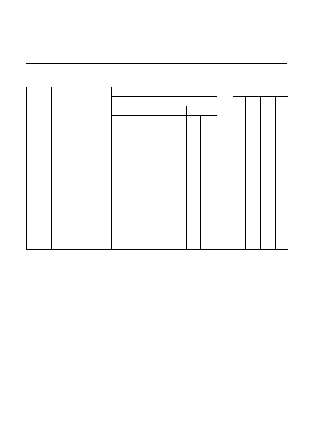
Fig.7 Test circuit for measuring OFF-state current.
handbook, full pagewidth
MGR260
AA
nY
nZ
VI = VCC or GND
VO = GND or V
CC
LOW
(from enable inputs)
GND
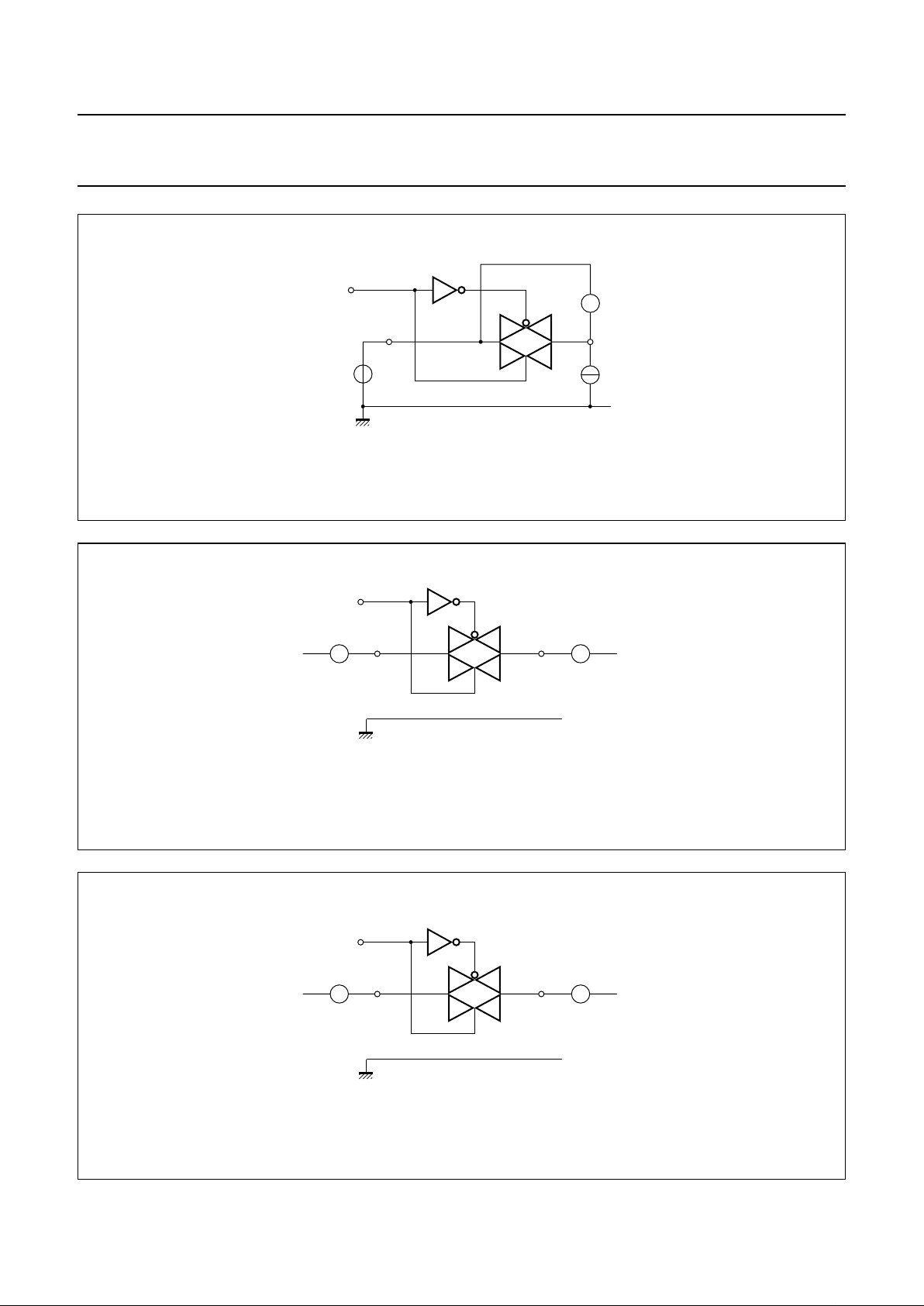
Fig.8 Test circuit for measuring ON-state current.
handbook, full pagewidth
MGR261
AA
nY
nZ
VI = VCC or GND
VO (open circuit)
HIGH
(from enable inputs)
GND

1998 Nov 10 8
Philips Semiconductors Product specification
Quad bilateral switches 74HC/HCT4066
Fig.9 Typical ON-resistance (RON) as a function of input voltage (Vis) for Vis= 0 to VCC.
handbook, halfpage
09
60
10
20
MGR262
30
40
50
1.8 3.6 5.4 7.2
Vis (V)
R
ON
(Ω)
6 V
9 V
VCC = 4.5 V
 Loading...