


MC78BC50NTR
T
30° to +80°C
SOT–23
Order this document by MC78BC00/D
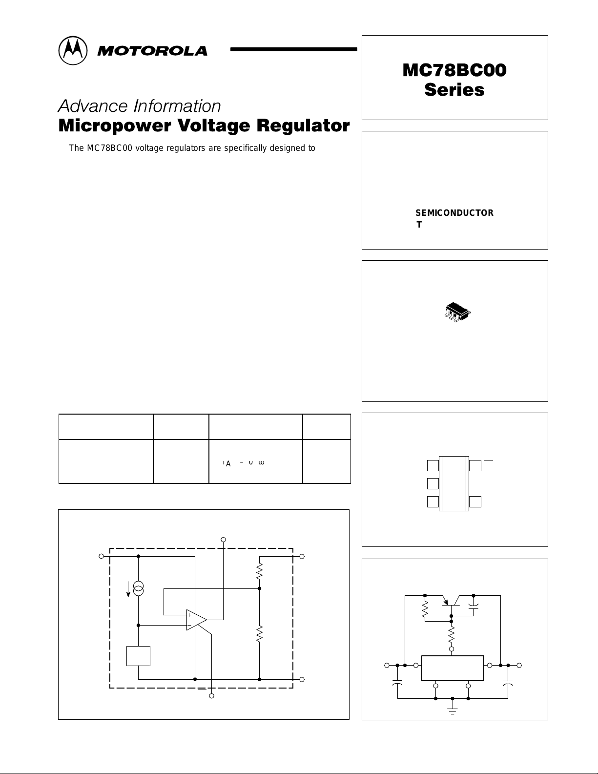
The MC78BC00 voltage regulators are specifically designed to be used
with an external power transistor to deliver high current with high voltage
accuracy and low quiescent current.
The MC78BC00 series are devices suitable for constructing regulators
with ultra–low dropout voltage and output current in the range of several tens
of mA to hundreds of mA. These devices have a chip enable function, which
minimizes the standby mode current drain. Each of these devices contains a
voltage reference unit, an error amplifier, a driver transistor and feedback
resistors. These devices are available in the SOT–23, 5 pin surface mount
packages.
These devices are ideally suited for battery powered equipment, and
power sources for hand–held audio instruments, communication equipment
and domestic appliances.
MC78BC00 Series Features:
• Ultra–Low Supply Current (50 µA)
• Standby Mode (0.2 µA)
• Ultra–Low Dropout Voltage (0.1 V with External Transistor and
IO = 100 mA)
• Excellent Line Regulation (Typically 0.1%/V)
• High Accuracy Output Voltage (±2.5%)
ORDERING INFORMATION
Output
Device
MC78BC30NTR 3.0
MC78BC33NTR 3.3
MC78BC40NTR 4.0
MC78BC50NTR 5.0
Other voltages from 2.0 to 6.0 V , in 0.1 V increments, are available. Consult factory for
information.
Voltage
Operating
Temperature Range
–
°
A
= –
°
Package
–
VOLTAGE REGULATOR
WITH EXTERNAL POWER
TRANSISTOR
SEMICONDUCTOR
TECHNICAL DATA
5
1
N SUFFIX
PLASTIC PACKAGE
CASE 1212
(SOT–23)
PIN CONNECTIONS
15
Ground
Input
Output
2
3
CE
Ext
4
Representative Block Diagram
2
V
in
V
ref
This device contains 13 active transistors.
This document contains information on a new product. Specifications and information herein
are subject to change without notice.
MOTOROLA ANALOG IC DEVICE DATA
4Ext
5CE
(Top View)
3
V
O
Standard Application
Q
C
C
Input Output
1
Gnd
Motorola, Inc. 1996 Rev 0
2
C
in
4
MC78BCXX
1
3
C
5
O
1
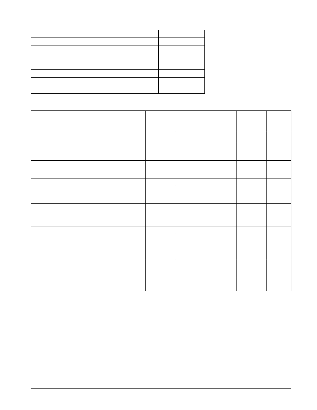
MC78BC00 Series
MAXIMUM RATINGS (T
Input Voltage V
Power Dissipation and Thermal Characteristics
Maximum Power Dissipation mW
Case 1212 (SOT–23) H Suffix P
Thermal Resistance, Junction–to–Ambient R
Operating Junction Temperature T
Operating Ambient Temperature T
Storage Temperature Range T
NOTE: ESD data available upon request.
ELECTRICAL CHARACTERISTICS (V
Output Voltage V
MC78BC30NTR 2.925 3.0 3.075
MC78BC33NTR 3.218 3.3 3.382
MC78BC40NTR 3.900 4.0 4.100
MC78BC50NTR 4.875 5.0 5.125
Line Regulation Reg
VO + 0.5 V ≤ Vin ≤ 8.0 V
Load Regulation Reg
Vin – VO = 1.0 V
1.0 mA ≤ lO ≤ 100 mA
Output Current (Note 2) l
Vin – VO = 1.0 V
Dropout Voltage Vin – V
IO = 100 mA
Supply Current l
Vin = 8.0 V
Vin – VO = 1.0 V
IO = 0 (at no load)
Supply Current (Standby) l
Vin = 8.0 V
Ext Leakage Current l
Chip Enable Input Logic Voltage V
Logic “0” (Regulator “On”) 0 – 0.25
Logic “1” (Regulator “Off”) 1.5 – 8.0
Chip Enable Input Current l
VCE = 0.25 V –5.0 –3.0 –0.1
VCE = 1.5 V – – 0.1
Output Voltage Temperature Coefficient T
NOTES: 1. Low duty pulse techniques are used during test to maintain junction temperature as close to ambient as possible.
2. The output current depends upon the performance of External PNP Transistor. Use External PNP Transistor of a low saturation type,
with an HFE of 100 or more.
= 25°C, unless otherwise noted.)
C
Rating
in
Characteristic
Symbol Value Unit
CC
D
θJA
J
A
stg
= VO + 1.0 V, IO = 50 mA, TJ = 25°C [Note 1], unless otherwise noted.)
Symbol Min Typ Max Unit
standby
10 Vdc
150
333 °C/W
125 °C
–30 to +80 °C
–40 to +125 °C
O
line
load
O
O
ss
LK
CE
CEL
C
0 0.1 0.3 mV
– 40 60 mV
– 1000 – mA
– 100 200 mV
– 50 80 µA
0.1 0.2 1.0 µA
– – 0.5 µA
– ±100 – ppm/°C
V
V
µA
2
MOTOROLA ANALOG IC DEVICE DATA

MC78BC00 Series
DEFINITIONS
Dropout Voltage – The input/output voltage differential at
which the regulator output no longer maintains regulation
against further reductions in input voltage. Measured when
the output drops 100 mV below its nominal value (which is
measured at 1.0 V differential), dropout voltage is affected by
junction temperature, load current and minimum input supply
requirements.
Line Regulation – The change in output voltage for a
change in input voltage. The measurement is made under
conditions of low dissipation or by using pulse techniques
Figure 1. Output V oltage versus Input Voltage
3.2
IO = 0 mA
3.0
IO = 100 mA
IO = 500 mA
4.0
5.0
Vin, INPUT VOLTAGE (V)
6.0
MC78BC30NTR
°
C
TA = 25
8.0 9.0 400 600
7.0
, OUTPUT VOL TAGE (V)
V
2.8
2.6
O
2.4
2.2
2.0
such that average chip temperature is not significantly
affected.
Load Regulation – The change in output voltage for a
change in load current at constant chip temperature.
Maximum Power Dissipation – The maximum total device
dissipation for which the regulator will operate within
specifications.
Supply Current – Current which is used to operate the
regulator chip and is not delivered to the load.
Figure 2. Output Voltage versus Output Current
4.962
Vin = 6.0 V
Vin = 5.1 V
500
, OUTPUT VOL TAGE (V)
V
O
4.958
4.954
4.950
4.946
4.942
0
MC78BC50NTR
& MJD32C
°
C
TA = 25
1003.0
IO, OUTPUT CURRENT (mA)
200
300
Figure 3. Dropout Voltage versus Output Current
0.50
0.40
0.30
0.20
, DROPOUT VOLTAGE (mV)
O
–V
0.10
in
V
0
0
TA = 25°C
MC78BC50NTR & MJD32C
200
400
IO, OUTPUT CURRENT (mA)
600
TA = 80°C
TA = –30°C
800
1000
Figure 4. Ripple Rejection as a
Function of Frequency
60
50
40
30
20
CL = 10 µF
RR, RIPPLE REJECTION (dB)
IO = 200 mA
10
0
1.0 k
°
C
TA = 25
MC78BC50NTR & MJD32C
10 k
100 k
f, FREQUENCY (Hz)
1.0 M
10 M1200
100 M
MOTOROLA ANALOG IC DEVICE DATA
3
 Loading...