


MC78L24ACPRP
MOTOROLA MC78L24ACPRP, MC78L24ABPRP, MC78L24ABP, MC78L18ACPRA, MC78L18ACPRM Datasheet
...
Semiconductor Components Industries, LLC, 1999
October, 1999 – Rev. 0
1 Publication Order Number:
MC78L00A/D
MC78L00A Series
Three-Terminal Low Current
Positive Voltage Regulators
The MC78L00A Series of positive voltage regulators are
inexpensive, easy–to–use devices suitable for a multitude of
applications that require a regulated supply of up to 100 mA. Like
their higher powered MC7800 and MC78M00 Series cousins, these
regulators feature internal current limiting and thermal shutdown
making them remarkably rugged. No external components are
required with the MC78L00 devices in many applications.
These devices offer a substantial performance advantage over the
traditional zener diode–resistor combination, as output impedance
and quiescent current are substantially reduced.
• Wide Range of Available, Fixed Output Voltages
• Low Cost
• Internal Short Circuit Current Limiting
• Internal Thermal Overload Protection
• No External Components Required
• Complementary Negative Regulators Offered (MC79L00A Series)
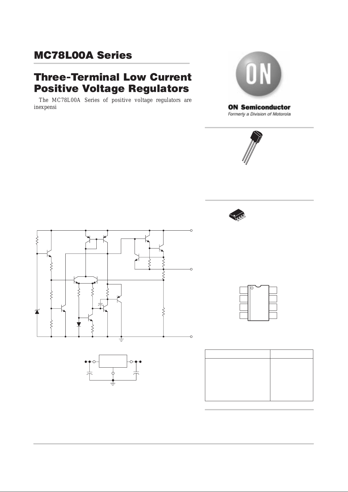
Representative Schematic Diagram
15k
Q1
Q3 Q5
Input
Output
Ground
Q11
Q12
3.0
0–25k
2.85k
5.0k
Q10
3.8k
Q4 Q6
1.2k
1.9k 19k 2.2k
Q9
Q8
C
Q7
1.0k
420
Z1
Q2
Standard Application
A common ground is required between the input and the output voltages. The
input voltage must remain typically 2.0 V above the output voltage even during
the low point on the input ripple voltage.
*C
in
is required if regulator is located an *appreciable distance from power
supply filter.
**C
O
is not needed for stability; however, it does *improve transient response.
MC78LXXA
Input
C
in
*
0.33µF
C
O
**
Output
TO–92
P SUFFIX
CASE 29
http://onsemi.com
See detailed ordering and shipping information in the package
dimensions section on page 7 of this data sheet.
ORDERING INFORMATION
2
3
1
Pin: 1. Output
2. Ground
3. Input
8
1
PIN CONNECTIONS
18
7
6
5
2
3
4
(Top View)
V
OUT
GND
GND
V
IN
GND
NC
GND
NC
SOP–8*
D SUFFIX
CASE 751
*SOP–8 is an internally modified SO–8 package. Pins
2, 3, 6, and 7 are electrically common to the die attach
flag. This internal lead frame modification decreases
package thermal resistance and increases power
dissipation capability when appropriately mounted on
a printed circuit board. SOP–8 conforms to all exter-
nal dimensions of the standard SO–8 package.
DEVICE TYPE/NOMINAL VOLTAGE
5% Output Voltage Accuracy Voltage
MC78L05AC
MC78L08AC
MC78L09AC
MC78L12AC
MC78L15AC
MC78L18AC
MC78L24AC
5.0
8.0
9.0
12
15
18
24
MC78L00A Series
http://onsemi.com
2
MAXIMUM RATINGS (T
A
= +125°C, unless otherwise noted.)
Rating
Symbol Value Unit
Input Voltage (2.6 V–8.0 V)
Input Voltage (12 V–18 V)
Input Voltage (24 V)
V
I
30
35
40
Vdc
Storage Temperature Range T
stg
–65 to +150 °C
Operating Junction Temperature Range T
J
0 to +150 °C
ELECTRICAL CHARACTERISTICS (V
I
= 10 V, I
O
= 40 mA, C
I
= 0.33 µF, C
O
= 0.1 µF, – 40°C < T
J
< +125°C (for MC78LXXAB),
0°C < T
J
< +125°C (for MC78LXXAC), unless otherwise noted.)
MC78L05AC, AB
Characteristics Symbol Min Typ Max Unit
Output Voltage (T
J
= +25°C) V
O
4.8 5.0 5.2 Vdc
Line Regulation
(T
J
= +25°C, I
O
= 40 mA)
7.0 Vdc ≤ V
I
≤ 20 Vdc
8.0 Vdc ≤ V
I
≤ 20 Vdc
Reg
line
–
–
55
45
150
100
mV
Load Regulation
(T
J
= +25°C, 1.0 mA ≤ I
O
≤ 100 mA)
(T
J
= +25°C, 1.0 mA ≤ I
O
≤ 40 mA)
Reg
load
–
–
11
5.0
60
30
mV
Output Voltage
(7.0 Vdc ≤ V
I
≤ 20 Vdc, 1.0 mA ≤ I
O
≤ 40 mA)
(V
I
= 10 V, 1.0 mA ≤ I
O
≤ 70 mA)
V
O
4.75
4.75
–
–
5.25
5.25
Vdc
Input Bias Current
(T
J
= +25°C)
(T
J
= +125°C)
I
IB
–
–
3.8
–
6.0
5.5
mA
Input Bias Current Change
(8.0 Vdc ≤ V
I
≤ 20 Vdc)
(1.0 mA ≤ I
O
≤ 40 mA)
∆I
IB
–
–
–
–
1.5
0.1
mA
Output Noise Voltage
(T
A
= +25°C, 10 Hz ≤ f ≤ 100 kHz)
V
n
– 40 – µV
Ripple Rejection (I
O
= 40 mA,
f = 120 Hz, 8.0 Vdc ≤ V
I
≤ 18 V, T
J
= +25°C)
RR 41 49 – dB
Dropout Voltage (T
J
= +25°C) V
I
– V
O
– 1.7 – Vdc
MC78L00A Series
http://onsemi.com
3
ELECTRICAL CHARACTERISTICS (V
I
= 14 V, I
O
= 40 mA, C
I
= 0.33 µF, C
O
= 0.1 µF, – 40°C < T
J
< +125°C (for MC78LXXAB),
0°C < T
J
< +125°C (for MC78LXXAC), unless otherwise noted.)
MC78L08AC, AB
Characteristics Symbol Min Typ Max Unit
Output Voltage (T
J
= +25°C) V
O
7.7 8.0 8.3 Vdc
Line Regulation
(T
J
= +25°C, I
O
= 40 mA)
10.5 Vdc ≤ V
I
≤ 23 Vdc
11 Vdc ≤ V
I
≤ 23 Vdc
Reg
line
–
–
20
12
175
125
mV
Load Regulation
(T
J
= +25°C, 1.0 mA ≤ I
O
≤ 100 mA)
(T
J
= +25°C, 1.0 mA ≤ I
O
≤ 40 mA)
Reg
load
–
–
15
8.0
80
40
mV
Output Voltage
(10.5 Vdc ≤ V
I
≤ 23 Vdc, 1.0 mA ≤ I
O
≤ 40 mA)
(V
I
= 14 V, 1.0 mA ≤ I
O
≤ 70 mA)
V
O
7.6
7.6
–
–
8.4
8.4
Vdc
Input Bias Current
(T
J
= +25°C)
(T
J
= +125°C)
I
IB
–
–
3.0
–
6.0
5.5
mA
Input Bias Current Change
(11 Vdc ≤ V
I
≤ 23 Vdc)
(1.0 mA ≤ I
O
≤ 40 mA)
∆I
IB
–
–
–
–
1.5
0.1
mA
Output Noise Voltage
(T
A
= +25°C, 10 Hz ≤ f ≤ 100 kHz)
V
n
– 60 – µV
Ripple Rejection (I
O
= 40 mA,
f = 120 Hz, 12 V ≤ V
I
≤ 23 V, T
J
= +25°C)
RR 37 57 – dB
Dropout Voltage (T
J
= +25°C) V
I
– V
O
– 1.7 – Vdc
ELECTRICAL CHARACTERISTICS (V
I
= 15 V, I
O
= 40 mA, C
I
= 0.33 µF, C
O
= 0.1 µF, – 40°C < T
J
< +125°C (for MC78LXXAB),
0°C < T
J
< +125°C (for MC78LXXAC), unless otherwise noted.)
MC78L09AC, AB
Characteristics Symbol Min Typ Max Unit
Output Voltage (T
J
= +25°C) V
O
8.6 9.0 9.4 Vdc
Line Regulation
(T
J
= +25°C, I
O
= 40 mA)
11.5 Vdc ≤ V
I
≤ 24 Vdc
12 Vdc ≤ V
I
≤ 24 Vdc
Reg
line
–
–
20
12
175
125
mV
Load Regulation
(T
J
= +25°C, 1.0 mA ≤ I
O
≤ 100 mA)
(T
J
= +25°C, 1.0 mA ≤ I
O
≤ 40 mA)
Reg
load
–
–
15
8.0
90
40
mV
Output Voltage
(11.5 Vdc ≤ V
I
≤ 24 Vdc, 1.0 mA ≤ I
O
≤ 40 mA)
(V
I
= 15 V, 1.0 mA ≤ I
O
≤ 70 mA)
V
O
8.5
8.5
–
–
9.5
9.5
Vdc
Input Bias Current
(T
J
= +25°C)
(T
J
= +125°C)
I
IB
–
–
3.0
–
6.0
5.5
mA
Input Bias Current Change
(11 Vdc ≤ V
I
≤ 23 Vdc)
(1.0 mA ≤ I
O
≤ 40 mA)
∆I
IB
–
–
–
–
1.5
0.1
mA
Output Noise Voltage
(T
A
= +25°C, 10 Hz ≤ f ≤ 100 kHz)
V
n
– 60 – µV
Ripple Rejection (I
O
= 40 mA,
f = 120 Hz, 13 V ≤ V
I
≤ 24 V, T
J
= +25°C)
RR 37 57 – dB
Dropout Voltage
(T
J
= +25°C)
V
I
– V
O
– 1.7 – Vdc
 Loading...