


October 1986
Revised March 2000
DM74AS646 • DM74AS648
Octal Bus Transceiver and Register
General Description
This device incorporates an octal bus transceiver and an octal D-type register configured to enable multiplexed transmission of data from bus to bus or internal register to bus.
This bus transceiver features totem-pole 3-STATE outputs designed specifically for driving highly-capacitive or relatively low-impedance loads. The high-impedance third state and increased high-logic-level drive provide this device with the capability of being connected directly to and driving the bus lines in a bus-organized system without need for interface or pull-up components. It is particularly attractive for implementing buffer registers, I/O ports, bidirectional bus drivers, and working registers.
The registers in the DM74AS646, DM74AS648 are edgetriggered D-type flip-flops. On the positive transition of the clock (CAB or CBA), the input bus data is stored.
The SAB and SBA control pins are provided to select whether real-time data or stored data is transferred. A LOW input level selects real-time data, and a HIGH level selects stored data. The select controls have a “make before break” configuration to eliminate a glitch which would normally occur in a typical multiplexer during the transition between stored and real-time data.
The enable G and direction control pins provide four modes of operation; real-time data transfer from bus A to B, realtime data transfer from bus B to A, real-time bus A and/or B data transfer to internal storage, or internal store data transfer to bus A or B.
When the enable G pin is LOW, the direction pin selects which bus receives data. When the enable G pin is HIGH, both buses become disabled yet their input function is still enabled.
Features
■Switching specifications at 50 pF
■Switching specifications guaranteed over full temperature and VCC range
■Advanced oxide-isolated, ion-implanted Schottky TTL process
■Functionally and pin-for-pin compatible with LS TTL counterpart
■3-STATE buffer-type outputs drive bus lines directly
Ordering Code:
Order Number |
Package Number |
Package Description |
|
|
|
DM74AS646WM |
M24B |
24-Lead Small Outline Integrated Circuit (SOIC), JEDEC MS-013, 0.300 Wide |
|
|
|
DM74AS646NT |
N24C |
24-Lead Plastic Dual-In-Line Package (PDIP), JEDEC MS-100, 0.300 Wide |
|
|
|
DM74AS648WM |
M24B |
24-Lead Small Outline Integrated Circuit (SOIC), JEDEC MS-013, 0.300 Wide |
|
|
|
DM74AS648NT |
N24C |
24-Lead Plastic Dual-In-Line Package (PDIP), JEDEC MS-100, 0.300 Wide |
|
|
|
Devices also available in Tape and Reel. Specify by appending the suffix letter “X” to the ordering code.
Register and Transceiver Bus Octal DM74AS648 • DM74AS646
© 2000 Fairchild Semiconductor Corporation |
DS006324 |
www.fairchildsemi.com |
DM74AS646 • DM74AS648
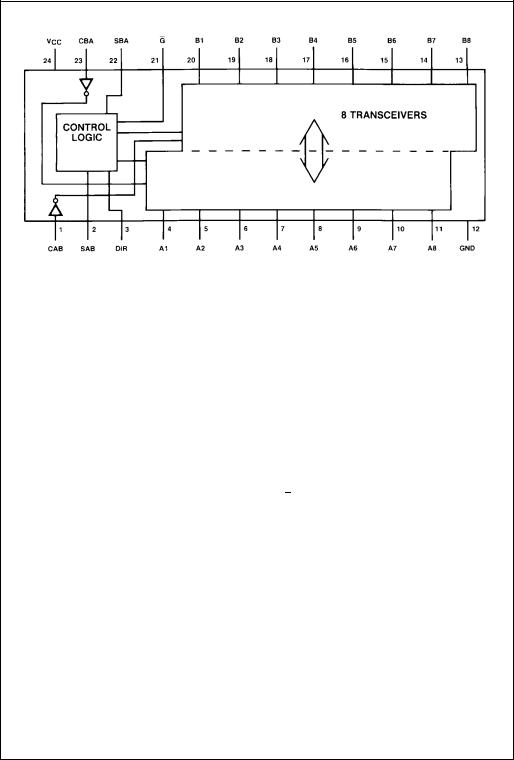
Connection Diagram
Function Table
|
|
|
|
Inputs |
|
|
Data I/O (Note 1) |
Operation or Function |
||||||||
|
|
|
|
|
|
|
|
|
|
|
|
|
|
|
||
G |
DIR |
CAB |
CBA |
SAB |
SBA |
A1 thru A8 |
B1 thru B8 |
DM74AS646 |
|
DM74AS648 |
||||||
|
|
|
|
|
|
|
|
|
|
|
||||||
|
H |
X |
H or L |
H or L |
X |
X |
Input |
Input |
Isolation, Hold Storage |
Isolation, Hold Storage |
||||||
|
|
|
X |
− |
− |
X |
X |
|
|
Store A and B Data |
Store A and B Data |
|||||
|
|
|
|
|
|
|
|
|
|
|
|
|
|
|||
|
L |
L |
X |
X |
X |
L |
Output |
Input |
Real Time B Data to A Bus |
Real Time |
|
|
Data to A Bus |
|||
|
B |
|||||||||||||||
|
|
|
|
|
|
|
|
|
|
|
|
|
||||
|
|
|
L |
X |
H or L |
X |
H |
|
|
Stored B Data to A Bus |
Stored |
B |
Data to A Bus |
|||
|
|
|
|
|
|
|
|
|
|
|
||||||
|
L |
H |
X |
X |
L |
X |
Input |
Output |
Real Time A Data to B Bus |
Real Time |
|
Data to B Bus |
||||
|
A |
|||||||||||||||
|
|
|
|
|
|
|
|
|
|
|
|
|||||
|
|
|
H |
H or L |
X |
H |
X |
|
|
Stored A Data to B Bus |
Stored |
A |
Data to B Bus |
|||
|
|
|
|
|
|
|
|
|
|
|
|
|||||
|
X |
X |
− |
X |
X |
X |
Input |
Unspecified |
Store A, B Unspecified |
Store A, B Unspecified |
||||||
|
(Note 1) |
(Note 1) |
(Note 1) |
|||||||||||||
|
|
|
|
|
|
|
|
|
||||||||
|
X |
X |
X |
− |
X |
X |
Unspecified |
Input |
Store B, A Unspecified |
Store B, A Unspecified |
||||||
|
(Note 1) |
(Note 1) |
(Note 1) |
|||||||||||||
|
|
|
|
|
|
|
|
|
||||||||
|
|
|
|
|
|
|
|
|
|
|
|
|
|
|||
H—HIGH level; L—LOW level; X—irrelevant; |
−—LOW-to-HIGH level transition |
|
|
|
|
|
|
|
||||||||
Note 1: The data output functions may be enabled or disabled by various signals at the G and DIR inputs. Data input functions are always enabled, i.e., data at the bus pins will be stored on every LOW-to-HIGH transition on the clock inputs.
www.fairchildsemi.com |
2 |

Logic Diagrams
(positive logic)
DM74AS646 |
DM74AS648 |
Different Modes of Control for DM74AS646, DM74AS648
Storage From A, B or A and B |
Transfer Stored Data to A or B |
|
(Note 2) |
Real-Time Transfer Bus A to Bus B |
Real-Time Transfer Bus B to Bus A |
(Note 2) |
(Note 2) |
Note 2: The complement of A and B data are stored and transferred for DM74AS648
DM74AS648 • DM74AS646
3 |
www.fairchildsemi.com |
 Loading...