


MOTOROLA MC33269ST-3.3T3, MC33269T, MC33269DTRK-3.3, MC33269DTRK-5.0, MC33269DT-3.3 Datasheet
...MC33269
Low Dropout Positive Fixed
and Adjustable Voltage
Regulators
The MC33269 series are low dropout, medium current, fixed and adjustable, positive voltage regulators specifically designed for use in low input voltage applications. These devices offer the circuit designer an economical solution for precision voltage regulation, while keeping power losses to a minimum.
The regulator consists of a 1.0 V dropout composite PNP±NPN pass transistor, current limiting, and thermal shutdown.
•3.3 V, 5.0 V, 12 V and Adjustable Versions.
2.85 V version available as MC34268.
•Space Saving DPAK, SOP±8 and SOT±223 Power Packages
•1.0 V Dropout
•Output Current in Excess of 800 mA
•Thermal Protection
•Short Circuit Protection
•Output Trimmed to 1.0% Tolerance
DEVICE TYPE / NOMINAL OUTPUT VOLTAGE
MC33269D |
Adj |
MC33269D±5.0 |
5.0 V |
MC33269DT |
Adj |
MC33269DT±5.0 |
5.0 V |
MC33269T |
Adj |
MC33269T±5.0 |
5.0 V |
MC33269D±3.3 |
3.3 V |
MC33269D±12 |
12 V |
MC33269DT±3.3 |
3.3 V |
MC33269DT±12 |
12 V |
MC33269T±3.3 |
3.3 V |
MC33269T±12 |
12 V |
MC33269ST±3.3 |
3.3 V |
|
|
|
|
|
|
http://onsemi.com
|
|
SOP±8 |
||
8 |
|
D SUFFIX |
||
1 |
|
CASE 751 |
||
|
|
|
||
Gnd/Adj |
1 |
8 |
NC |
|
Vout |
2 |
7 |
Vout |
|
3 |
6 |
|||
|
|
|||
Vin |
4 |
5 |
NC |
|
|
|
(Top View) |
|
|
|
|
DPAK |
|
|
DT SUFFIX |
|
1 |
CASE 369A |
|
3 |
|
|
1. |
Gnd/Adj |
|
2. |
Vout |
1 2 3 |
3. |
Vin |
SOT±223
(Top View) ST SUFFIX
CASE 318E
1
3
Heatsink surface (shown as terminal 4 in case outline drawing) is connected to Pin 2.
TO±220AB
T SUFFIX
CASE 221A
1 |
2 |
Pin: |
1. |
Gnd/Adj |
|
||||
|
3 |
2. |
Vout |
|
|
|
|||
|
|
|
3. |
Vin |
|
|
1 2 3 |
|
|
|
|
(Top View) |
|
|
|
|
Heatsink surface (shown as terminal 4 in |
|
|
case outline drawing) is connected to Pin 2. |
|
|
|
|
|
ORDERING INFORMATION |
|
|
See detailed ordering and shipping information in the package |
|
|
dimensions section on page 7 of this data sheet. |
|
|
|
Semiconductor Components Industries, LLC, 2000 |
1 |
Publication Order Number: |
April, 2000 ± Rev. 8 |
|
MC33269/D |

MC33269
MAXIMUM RATINGS
Rating |
Symbol |
Value |
Unit |
|
|
|
|
Power Supply Input Voltage |
Vin |
20 |
V |
Power Dissipation |
|
|
|
Case 369A (DPAK) |
|
|
|
TA = 25°C |
PD |
Internally Limited |
W |
Thermal Resistance, Junction±to±Ambient |
θJA |
92 |
°C/W |
Thermal Resistance, Junction±to±Case |
θJC |
6.0 |
°C/W |
Case 751 (SOP±8) |
|
|
|
TA = 25°C |
PD |
Internally Limited |
W |
Thermal Resistance, Junction±to±Ambient |
θJA |
160 |
°C/W |
Thermal Resistance, Junction±to±Case |
θJC |
25 |
°C/W |
Case 221A |
|
|
|
TA = 25°C |
PD |
Internally Limited |
W |
Thermal Resistance, Junction±to±Ambient |
θJA |
65 |
°C/W |
Thermal Resistance, Junction±to±Case |
θJC |
5.0 |
°C/W |
Case 318E |
|
|
|
TA = 25°C |
PD |
Internally Limited |
W |
Thermal Resistance, Junction±to±Ambient |
θJA |
245 |
°C/W |
Thermal Resistance, Junction±to±Case |
θJC |
15 |
°C/W |
Operating Junction Temperature Range |
TJ |
±40 to +150 |
°C |
Storage Temperature |
Tstg |
±55 to +150 |
°C |
NOTE: ESD data available upon request.
ELECTRICAL CHARACTERISTICS (CO = 10 μF, TA = 25°C, for min/max values TJ = ±40°C to +125°C, unless otherwise noted.)
|
Characteristic |
Symbol |
Min |
Typ |
Max |
Unit |
|
|
|
|
|
|
|
Output Voltage (Iout = 10 mA, TJ = 25°C) |
VO |
|
|
|
V |
|
3.3 Suffix |
(VCC = 5.3 V) |
|
3.27 |
3.3 |
3.33 |
|
5.0 Suffix |
(VCC = 7.0 V) |
|
4.95 |
5.0 |
5.05 |
|
12 Suffix (VCC = 14 V) |
|
11.88 |
12 |
12.12 |
|
|
Output Voltage (Line, Load and Temperature) (Note 1.) |
VO |
|
|
|
V |
|
(1.25 V ≤ Vin ± Vout ≤ 15 V, Iout = 500 mA) |
|
|
|
|
|
|
(1.35 V ≤ Vin ± Vout ≤ 10 V, Iout = 800 mA) |
|
|
|
|
|
|
3.3 Suffix |
|
|
3.23 |
3.3 |
3.37 |
|
5.0 Suffix |
|
|
4.9 |
5.0 |
5.1 |
|
12 Suffix |
|
|
11.76 |
12 |
12.24 |
|
|
|
|
|
|
|
|
Reference Voltage (Iout = 10 mA, Vin ± Vout = 2.0 V, TJ = 25°C) |
Vref |
1.235 |
1.25 |
1.265 |
V |
|
for Adjustable Voltage |
|
|
|
|
|
|
|
|
|
|
|
|
|
Reference Voltage (Line, Load and Temperature) (Note 1.) |
Vref |
1.225 |
1.25 |
1.275 |
V |
|
(1.25 V ≤ Vin ± Vout ≤ 15 V, Iout = 500 mA) |
|
|
|
|
|
|
(1.35 V ≤ Vin ± Vout ≤ 10 V, Iout = 800 mA) |
|
|
|
|
|
|
for Adjustable Voltage |
|
|
|
|
|
|
|
|
|
|
|
|
|
Line Regulation |
Regline |
± |
± |
0.3 |
% |
|
(Iout = 10 mA, Vin = [Vout + 1.5 V] to Vin = 20 V, TJ = 25°C) |
|
|
|
|
|
|
Load Regulation (Vin = Vout + 3.0 V, Iout = 10 mA to 800 mA, TJ = 25°C) |
Regload |
± |
± |
0.5 |
% |
|
Dropout Voltage |
Vin ± Vout |
|
|
|
V |
|
(Iout = 500 mA) |
|
± |
1.0 |
1.25 |
|
|
(Iout = 800 mA) |
|
± |
1.1 |
1.35 |
|
|
Ripple Rejection |
RR |
55 |
± |
± |
dB |
|
(10 Vpp, 120 Hz Sinewave; Iout = 500 mA) |
|
|
|
|
|
|
Current Limit (Vin ± Vout = 10 V) |
ILimit |
800 |
± |
± |
mA |
|
Quiescent Current (Fixed Output) |
IQ |
|
|
|
mA |
|
(1.5 V ≤ Vout ≤ 3.3 V) |
|
± |
5.5 |
8.0 |
|
|
(5 V ≤ Vout ≤ 12 V) |
|
± |
± |
20 |
|
|
1. The MC33269±12, Vin ± Vout is limited to 8.0 V maximum, because of the 20 V maximum rating applied to Vin.
http://onsemi.com
2
MC33269
ELECTRICAL CHARACTERISTICS (CO = 10 μF, TA = 25°C, for min/max values TJ = ±40°C to +125°C, unless otherwise noted.)
Characteristic |
Symbol |
Min |
Typ |
Max |
Unit |
|
|
|
|
|
|
Minimum Required Load Current |
ILoad |
|
|
|
mA |
Fixed Output Voltage |
|
± |
± |
0 |
|
Adjustable Voltage |
|
8.0 |
± |
± |
|
|
|
|
|
|
|
Adjustment Pin Current |
IAdj |
± |
± |
120 |
μA |
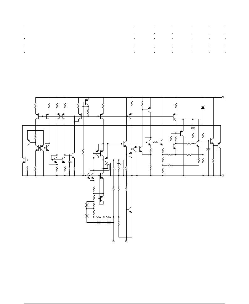
Internal Schematic |
Vin |
|
Vout
Trim Links
VAdj Gnd
This device contains 38 active transistors.
http://onsemi.com
3

MC33269
Vin±Vout , DROPOUT VOLTAGE (V)
1.5 |
|
|
1.3 |
|
|
1.1 |
TA = 25°C |
TA = ±40°C |
0.9 |
|
TA = 125°C |
0.7
0.5
0 |
200 |
400 |
600 |
800 |
1000 |
|
|
IO, OUTPUT LOAD CURRENT (mA) |
|
|
|
Figure 1. Dropout Voltage versus
Output Load Current
OUTPUT |
DEVIATION |
V |
VOLTAGE |
, |
|
O |
|
, OUTPUT |
CURRENT |
O |
|
I |
|
100
mV/Div
Cin = 10 μF
CO = 10 μF Tantalum
Vin = VO + 3.0 V
Preload = 0.1 A
0.5 A
0 A
20 ms/DIV
Figure 2. Transient Load Regulation
) |
|
|
|
|
|
|
|
|
|
FB |
|
|
|
|
|
|
|
|
|
(%V |
1100 |
|
|
|
|
|
|
|
1.6 |
OVERVOLTAGE INPUT THRESHOLD |
|
|
|
|
|
|
IO = 800 mA |
|
1.4 |
1060 |
|
|
|
|
|
|
OUTPUT CURRENT (A) |
1.2 |
|
|
|
|
|
|
|
|
|||
1020 |
|
|
|
|
|
|
1.0 |
||
|
|
|
|
|
|
|
|||
|
|
|
|
|
|
|
0.8 |
||
980 |
|
|
|
|
|
|
0.6 |
||
|
|
|
|
|
|
|
|||
940 |
|
|
|
|
|
|
0.4 |
||
|
|
|
|
|
|
|
|||
|
|
|
|
|
|
|
0.2 |
||
, |
|
|
|
|
|
|
|
|
|
FB(OV) |
900 |
|
|
|
|
|
|
|
0 |
±55 |
±25 |
0 |
25 |
50 |
75 |
100 |
125 |
|
|
V |
|
|
TA, AMBIENT TEMPERATURE (°C) |
|
|
||||
|
|
|
|
|
|||||
|
|
|
|
TA = 25°C |
|
|
|
|
|
|
|
|
MC33269D±XX |
|
|
|
|
|
|
|
|
L = 25 mm Copper |
|
|
|
|
0 |
2.0 |
4.0 |
6.0 |
8.0 |
10 |
12 |
14 |
16 |
INPUT±OUTPUT VOLTAGE DIFFERENTIAL (V)
Figure 3. Dropout Voltage |
Figure 4. MC33269±XX Output DC Current versus |
versus Temperature |
Input±Output Differential Voltage |
|
70 |
|
|
|
|
70 |
|
|
|
(dB) |
|
|
VO = 3.3 V or 5.0 V |
|
(dB) |
|
|
|
|
60 |
|
|
|
60 |
|
|
|
||
RATIO |
VO = 12 V |
|
RATIO |
|
|
|
|||
|
|
|
|
|
|
||||
REJECTION |
|
|
REJECTION |
|
|
|
|
||
40 |
Vin = VO + 3.0 V |
|
|
40 |
IL = 800 mA |
|
|
||
|
50 |
|
|
|
|
50 |
Vin = 8.0 V |
|
|
|
|
|
|
|
|
|
Vout = 5.0 V |
|
|
RIPPLE |
|
IL = 800 mA |
|
|
RIPPLE |
|
CAdj = 22 μF |
|
|
30 |
TA = 25°C |
|
|
|
TA = 25°C |
|
|
||
|
|
|
|
|
|
|
|||
RR, |
|
|
|
RR, |
30 |
|
|
|
|
|
|
|
|
|
|
|
|
||
|
20 |
1.0 |
10 |
100 |
|
20 |
1.0 |
10 |
100 |
|
0.1 |
|
0.1 |
||||||
|
|
|
f, FREQUENCY (kHz) |
|
|
|
|
f, FREQUENCY (kHz) |
|
Figure 5. MC33269 Ripple Rejection |
Figure 6. MC33269±ADJ Ripple Rejection |
versus Frequency |
versus Frequency |
http://onsemi.com
4
 Loading...