


MSP430F247TPM
Texas Instruments MSP430F247TPM, MSP430F233TRGC, MSP430F247TRGC, MSP430F2471TRGC, MSP430F2471TPM Manual
...
MSP430F23x
MSP430F24x(1)
MSP430F2410
www.ti.com
SLAS547I –JUNE 2007–REVISED DECEMBER 2012
MIXED SIGNAL MICROCONTROLLER
1
FEATURES
23
• Low Supply-Voltage Range, 1.8 V to 3.6 V
• Ultra-Low Power Consumption • Supply Voltage Supervisor/Monitor With
– Active Mode: 270 µA at 1 MHz, 2.2 V
– Standby Mode (VLO): 0.3 µA
– Off Mode (RAM Retention): 0.1 µA
• Ultra-Fast Wake-Up From Standby Mode in
Less Than 1 µs
• 16-Bit RISC Architecture, 62.5-ns Instruction
Cycle Time
• Basic Clock Module Configurations:
– Internal Frequencies up to 16 MHz
– Internal Very Low-Power LF Oscillator
– 32-kHz Crystal
– Internal Frequencies up to 16 MHz With
Four Calibrated Frequencies to ±1% – 2KB RAM
– Resonator – MSP430F247, MSP430F2471
– External Digital Clock Source – 32KB+256B Flash Memory
– External Resistor – 4KB RAM
• 12-Bit Analog-to-Digital (A/D) Converter With – MSP430F248, MSP430F2481
Internal Reference, Sample-and-Hold, and
Autoscan Feature
• 16-Bit Timer_A With Three Capture/Compare
Registers
• 16-Bit Timer_B With Seven Capture/Compare
With Shadow Registers
• Four Universal Serial Communication
Interfaces (USCI)
– USCI_A0 and USCI_A1
– Enhanced UART Supporting Auto-Baudrate
Detection
– IrDA Encoder and Decoder
– Synchronous SPI
– USCI_B0 and USCI_B1
– I2C™
– Synchronous SPI implemented on the MSP430F24x1.
• On-Chip Comparator
Programmable Level Detection
• Brownout Detector
• Bootstrap Loader
• Serial Onboard Programming, No External
Programming Voltage Needed, Programmable
Code Protection by Security Fuse
• Family Members Include:
– MSP430F233
– 8KB+256B Flash Memory,
– 1KB RAM
– MSP430F235
– 16KB+256B Flash Memory
(1)
– 48KB+256B Flash Memory
– 4KB RAM
– MSP430F249, MSP430F2491
– 60KB+256B Flash Memory
– 2KB RAM
– MSP430F2410
– 56KB+256B Flash Memory
– 4KB RAM
• Available in 64-Pin QFP and 64-Pin QFN
Packages (See Available Options)
• For Complete Module Descriptions, See
MSP430x2xx Family User’s Guide (SLAU144)
(1) The MSP430F24x1 devices are identical to the MSP430F24x
devices, with the exception that the ADC12 module is not
1
Please be aware that an important notice concerning availability, standard warranty, and use in critical applications of
Texas Instruments semiconductor products and disclaimers thereto appears at the end of this data sheet.
2MSP430 is a trademark of Texas Instruments.
3All other trademarks are the property of their respective owners.
PRODUCTION DATA information is current as of publication date.
Products conform to specifications per the terms of the Texas
Instruments standard warranty. Production processing does not
necessarily include testing of all parameters.
Copyright © 2007–2012, Texas Instruments Incorporated

MSP430F23x
MSP430F24x(1)
MSP430F2410
SLAS547I –JUNE 2007–REVISED DECEMBER 2012
This integrated circuit can be damaged by ESD. Texas Instruments recommends that all integrated circuits be handled with
appropriate precautions. Failure to observe proper handling and installation procedures can cause damage.
ESD damage can range from subtle performance degradation to complete device failure. Precision integrated circuits may be more
susceptible to damage because very small parametric changes could cause the device not to meet its published specifications.
DESCRIPTION
The Texas Instruments MSP430™ family of ultra-low power microcontrollers consists of several devices featuring
different sets of peripherals targeted for various applications. The architecture, combined with five low-power
modes, is optimized to achieve extended battery life in portable measurement applications. The device features a
powerful 16-bit RISC CPU, 16-bit registers, and constant generators that contribute to maximum code efficiency.
The calibrated digitally controlled oscillator (DCO) allows wake-up from low-power modes to active mode in less
than 1 µs.
The MSP430F23x, MSP430F24x(1), and MSP430F2410 series are microcontroller configurations with two builtin 16-bit timers, a fast 12-bit A/D converter (not MSP430F24x1), a comparator, four (two in MSP430F23x)
universal serial communication interface (USCI) modules, and up to 48 I/O pins. The MSP430F24x1 devices are
identical to the MSP430F24x devices, with the exception that the ADC12 module is not implemented. The
MSP430F23x devices are identical to the MSP430F24x devices, with the exception that a reduced Timer_B, one
USCI module, and less RAM are integrated.
Typical applications include sensor systems, industrial control applications, and hand-held meters.
www.ti.com
Table 1. Available Options
T
A
-40°C to 105°C MSP430F248TPM MSP430F248TRGC
(1) For the most current package and ordering information, see the Package Option Addendum at the end
of this document, or see the TI web site at www.ti.com.
(2) Package drawings, thermal data, and symbolization are available at www.ti.com/packaging.
PLASTIC 64-PIN QFP (PM) PLASTIC 64-PIN QFN (RGC)
MSP430F233TPM MSP430F233TRGC
MSP430F235TPM MSP430F235TRGC
MSP430F247TPM MSP430F247TRGC
MSP430F2471TPM MSP430F2471TRGC
MSP430F2481TPM MSP430F2481TRGC
MSP430F249TPM MSP430F249TRGC
MSP430F2491TPM MSP430F2491TRGC
MSP430F2410TPM MSP430F2410TRGC
PACKAGED DEVICES
(1)(2)
Development Tool Support
All MSP430 microcontrollers include an Embedded Emulation Module (EEM) allowing advanced debugging and
programming through easy to use development tools. Recommended hardware options include the following:
• Debugging and Programming Interface
– MSP-FET430UIF (USB)
– MSP-FET430PIF (Parallel Port)
• Debugging and Programming Interface with Target Board
– MSP-FET430U64 (PM package)
• Standalone Target Board
– MSP-TS430PM64 (PM package)
• Production Programmer
– MSP-GANG430
2 Submit Documentation Feedback Copyright © 2007–2012, Texas Instruments Incorporated
P1.7/TA2
AV
SS
P6.2/A2
P2.0/ACLK/CA2
P6.1/A1
P2.1/TAINCLK/CA3
P6.0/A0
P2.2/CAOUT/TA0/CA4
RST/NMI
P2.3/CA0/TA1
TCK
P2.4/CA1/TA2
TDO/TDI
P2.7/TA0/CA7
TDI/TCLK
P2.6/ADC12CLK/CA6
XT2IN
P3.0/UCB0STE/UCA0CLK
XT2OUT
P5.7/TBOUTH/SVSOUT
P3.2/UCB0SOMI/UCB0SCL
P5.6/ACLK
P3.3/UCB0CLK/UCA0STE
P5.5/SMCLK
P3.4/UCA0TXD/UCA0SIMO
P4.4
XOUT
P5.3
P6.3/A3
P5.4/MCLK
DV
CC
P5.2
P6.4/A4
P4.7/TBCLK
P6.7/A7/SVSIN
P5.1
P6.5/A5
P5.0
P6.6/A6
P4.6
V
REF+
P4.5XIN
P4.1/TB1P1.0/TACLK/CAOUT
P4.3Ve
REF+
P4.2/TB2V /Ve
REF- REF-
P4.0/TB0P1.1/TA0
P3.7P1.2/TA1
P3.5/UCA0RXD/UCA0SOMIP1.4/SMCLK
P3.6P1.3/TA2
TMS
P2.5/R /CA5
OSC
P1.6/TA1
DV
SS
P1.5/TA0
AV
CC
1962206121602259235824
57
27
54
2655285329523051315032
49
409
472
48
1
463
436
45
4
44
5
42
7
41
8
37
12
3910
38
11
3613
35
14
3316
3415
25
56
18
63
17
64
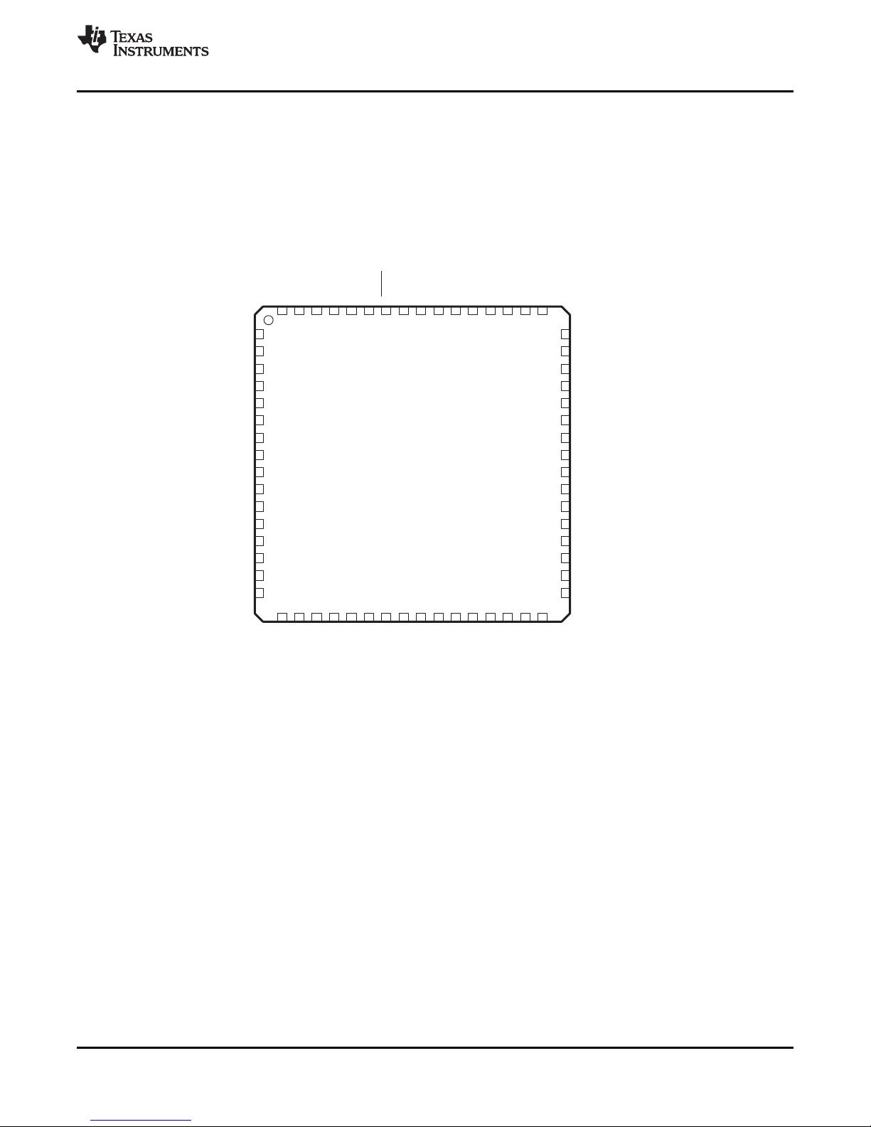
PM OR RGC PACKAGE
(TOP VIEW)
MSP430F23x
www.ti.com
Device Pinout, MSP430F23x
MSP430F23x
MSP430F24x(1)
MSP430F2410
SLAS547I –JUNE 2007–REVISED DECEMBER 2012
Copyright © 2007–2012, Texas Instruments Incorporated Submit Documentation Feedback 3

P1.7/TA2
AV
SS
P6.2/A2
P2.0/ACLK/CA2
P6.1/A1
P2.1/TAINCLK/CA3
P6.0/A0
P2.2/CAOUT/TA0/CA4
RST/NMI
P2.3/CA0/TA1
TCK
P2.4/CA1/TA2
TDO/TDI
P2.7/TA0/CA7
TDI/TCLK
P2.6/ADC12CLK/CA6
XT2IN
P3.0/UCB0STE/UCA0CLK
XT2OUT
P5.7/TBOUTH/SVSOUT
P3.2/UCB0SOMI/UCB0SCL
P5.6/ACLK
P3.3/UCB0CLK/UCA0STE
P5.5/SMCLK
P3.4/UCA0TXD/UCA0SIMO
P4.4/TB4
XOUT
P5.3/UCB1CLK/UCA1STE
P6.3/A3
P5.4/MCLK
DV
CC
P5.2/UCB1SOMI/UCB1SCL
P6.4/A4
P4.7/TBCLK
P6.7/A7/SVSIN
P5.1/UCB1SIMO/UCB1SDA
P6.5/A5
P5.0/UCB1STE/UCA1CLK
P6.6/A6
P4.6/TB6
V
REF+
P4.5/TB5XIN
P4.1/TB1P1.0/TACLK/CAOUT
P4.3/TB3Ve
REF+
P4.2/TB2V /Ve
REF- REF-
P4.0/TB0P1.1/TA0
P3.7/UCA1RXD/UCA1SOMIP1.2/TA1
P3.5/UCA0RXD/UCA0SOMIP1.4/SMCLK
P3.6/UCA1TXD/UCA1SIMO
P1.3/TA2
TMS
P2.5/R /CA5
OSC
P1.6/TA1
DV
SS
P1.5/TA0
AV
CC
1962206121602259235824
57
27
54
2655285329523051315032
49
409
472
48
1
463
436
45
4
44
5
42
7
41
8
37
12
3910
38
11
3613
35
14
3316
3415
25
56
18
63
17
64
PM OR RGC PACKAGE
(TOP VIEW)
MSP430F2410,
MSP430F24x
MSP430F23x
MSP430F24x(1)
MSP430F2410
SLAS547I –JUNE 2007–REVISED DECEMBER 2012
Device Pinout, MSP430F24x, MSP430F2410
www.ti.com
4 Submit Documentation Feedback Copyright © 2007–2012, Texas Instruments Incorporated

P1.7/TA2
AV
SS
P6.2
P2.0/ACLK/CA2
P6.1
P2.1/TAINCLK/CA3
P6.0
P2.2/CAOUT/TA0/CA4
RST/NMI
P2.3/CA0/TA1
TCK
P2.4/CA1/TA2
TDO/TDI
P2.7/TA0/CA7
TDI/TCLK
P2.6/ADC12CLK/CA6
XT2IN
P3.0/UCB0STE/UCA0CLK
XT2OUT
P5.7/TBOUTH/SVSOUT
P3.2/UCB0SOMI/UCB0SCL
P5.6/ACLK
P3.3/UCB0CLK/UCA0STE
P5.5/SMCLK
P3.4/UCA0TXD/UCA0SIMO
P4.4/TB4
XOUT
P5.3/UCB1CLK/UCA1STE
P6.3
P5.4/MCLK
DV
CC
P5.2/UCB1SOMI/UCB1SCL
P6.4
P4.7/TBCLK
P6.7/A7/SVSIN
P5.1/UCB1SIMO/UCB1SDA
P6.5
P5.0/UCB1STE/UCA1CLK
P6.6
P4.6/TB6
V
REF+
P4.5/TB5XIN
P4.1/TB1P1.0/TACLK/CAOUT
P4.3/TB3DV
SS
P4.2/TB2DV
SS
P4.0/TB0P1.1/TA0
P3.7/UCA1RXD/UCA1SOMIP1.2/TA1
P3.5/UCA0RXD/UCA0SOMIP1.4/SMCLK
P3.6/UCA1TXD/UCA1SIMO
P1.3/TA2
TMS
P2.5/R /CA5
OSC
P1.6/TA1
DV
SS
P1.5/TA0
AV
CC
1962206121602259235824
57
27
54
2655285329523051315032
49
409
472
48
1
463
436
45
4
44
5
42
7
41
8
37
12
3910
38
11
3613
35
14
3316
3415
25
56
18
63
17
64
PM OR RGC PACKAGE
(TOP VIEW)
MSP430F24x1
www.ti.com
Device Pinout, MSP430F24x1
MSP430F23x
MSP430F24x(1)
MSP430F2410
SLAS547I –JUNE 2007–REVISED DECEMBER 2012
Copyright © 2007–2012, Texas Instruments Incorporated Submit Documentation Feedback 5

Oscillators
Basic Clock
System+
RAM
2kB
1kB
BOR
SVS/SVM
RST/NMI
DVCC
DVSS
MCLK
Watchdog
WDT+
15/16-Bit
Timer_A3
3 CC
Registers
16MHz
CPU
incl. 16
Registers
Emulation
XOUT/
XT2OUT
JTAG
Interface
Ports
P1/P2
2x8 I/O
Interrupt
capability
USCI A0
UART/LIN,
IrDA, SPI
USCI B0
SPI, I2C
Comp_A+
Flash
16kB
8kB
Timer_B3
3 CC
Registers,
Shadow
Reg
ADC12
12-Bit
8
Channels
Ports
P3/P4
P5/P6
4x8 I/O
AVCC
AVSS
P1.x/P2.x
2x8
P3.x/P4.x
P5.x/P6.x
4x8
XIN/
XT2IN
22
SMCLK
ACLK
MDB
MAB
Hardware
Multiplier
MPY,
MPYS,
MAC,
MACS
MSP430F23x
MSP430F24x(1)
MSP430F2410
SLAS547I –JUNE 2007–REVISED DECEMBER 2012
Functional Block Diagram, MSP430F23x
www.ti.com
6 Submit Documentation Feedback Copyright © 2007–2012, Texas Instruments Incorporated

Oscillators
Basic Clock
System+
RAM
2kB
4kB
4kB
4kB
BOR
SVS/SVM
RST/NMI
DVCC
DVSS
MCLK
Watchdog
WDT+
15/16-Bit
Timer_A3
3 CC
Registers
16MHz
CPU
incl. 16
Registers
Emulation
XOUT/
XT2OUT
JTAG
Interface
Ports
P1/P2
2x8 I/O
Interrupt
capability
USCI A0
UART/LIN,
IrDA, SPI
USCI B0
SPI, I2C
Comp_A+
Flash
60kB
56kB
48kB
32kB
Timer_B7
7 CC
Registers,
Shadow
Reg
ADC12
12-Bit
8
Channels
Ports
P3/P4
P5/P6
4x8 I/O
AVCC
AVSS
P1.x/P2.x
2x8
P3.x/P4.x
P5.x/P6.x
4x8
XIN/
XT2IN
22
SMCLK
ACLK
MDB
MAB
Hardware
Multiplier
MPY,
MPYS,
MAC,
MACS
USCI A1
UART/LIN,
IrDA, SPI
USCI B1
SPI, I2C
www.ti.com
Functional Block Diagram, MSP430F24x, MSP430F2410
MSP430F23x
MSP430F24x(1)
MSP430F2410
SLAS547I –JUNE 2007–REVISED DECEMBER 2012
Copyright © 2007–2012, Texas Instruments Incorporated Submit Documentation Feedback 7

Oscillators
Basic Clock
System+
RAM
2kB
4kB
4kB
BOR
SVS/SVM
RST/NMI
DVCC
DVSS
MCLK
Watchdog
WDT+
15/16-Bit
Timer_A3
3 CC
Registers
16MHz
CPU
incl. 16
Registers
Emulation
XOUT/
XT2OUT
JTAG
Interface
Ports
P1/P2
2x8 I/O
Interrupt
capability
USCI A0
UART/LIN,
IrDA, SPI
USCI B0
SPI, I2C
Comp_A+
Flash
60kB
48kB
32kB
Timer_B7
7 CC
Registers,
Shadow
Reg
Ports
P3/P4
P5/P6
4x8 I/O
AVCC
AVSS
P1.x/P2.x
2x8
P3.x/P4.x
P5.x/P6.x
4x8
XIN/
XT2IN
22
SMCLK
ACLK
MDB
MAB
Hardware
Multiplier
MPY,
MPYS,
MAC,
MACS
USCI A1
UART/LIN,
IrDA, SPI
USCI B1
SPI, I2C
MSP430F23x
MSP430F24x(1)
MSP430F2410
SLAS547I –JUNE 2007–REVISED DECEMBER 2012
Functional Block Diagram, MSP430F24x1
www.ti.com
8 Submit Documentation Feedback Copyright © 2007–2012, Texas Instruments Incorporated

MSP430F23x
MSP430F24x(1)
MSP430F2410
www.ti.com
Table 2. Terminal Functions, MSP430F23x
TERMINAL
NAME NO.
AV
CC
AV
SS
DV
CC
DV
SS
P1.0/TACLK/CAOUT 12 I/O General-purpose digital I/O / Timer_A, clock signal TACLK input/Comparator_A output
P1.1/TA0 13 I/O General-purpose digital I/O / Timer_A, capture: CCI0A input, compare: Out0 output/BSL transmit
P1.2/TA1 14 I/O General-purpose digital I/O / Timer_A, capture: CCI1A input, compare: Out1 output
P1.3/TA2 15 I/O General-purpose digital I/O / Timer_A, capture: CCI2A input, compare: Out2 output
P1.4/SMCLK 16 I/O General-purpose digital I/O / SMCLK signal output
P1.5/TA0 17 I/O General-purpose digital I/O / Timer_A, compare: Out0 output
P1.6/TA1 18 I/O General-purpose digital I/O / Timer_A, compare: Out1 output
P1.7/TA2 19 I/O General-purpose digital I/O / Timer_A, compare: Out2 output
P2.0/ACLK/CA2 20 I/O General-purpose digital I/O / ACLK output/Comparator_A input
P2.1/TAINCLK/CA3 21 I/O General-purpose digital I/O / Timer_A, clock signal at INCLK
P2.2/CAOUT/TA0/CA4 22 I/O
P2.3/CA0/TA1 23 I/O General-purpose digital I/O / Timer_A, compare: Out1 output/Comparator_A input
P2.4/CA1/TA2 24 I/O General-purpose digital I/O / Timer_A, compare: Out2 output/Comparator_A input
P2.5/R
P2.6/ADC12CLK/CA6 26 I/O General-purpose digital I/O / conversion clock - 12-bit ADC/Comparator_A input
P2.7/TA0/CA7 27 I/O General-purpose digital I/O / Timer_A, compare: Out0 output/Comparator_A input
P3.0/UCB0STE/ UCA0CLK 28 I/O General-purpose digital I/O / USCI_B0 slave transmit enable/USCI A0 clock input/output
P3.1/UCB0SIMO/UCB0SDA 29 I/O
P3.2/UCB0SOMI/ UCB0SCL 30 I/O
P3.3/UCB0CLK/UCA0STE 31 I/O General-purpose digital I/O / USCI_B0 clock input/output, USCI A0 slave transmit enable
P3.4/UCA0TXD/ UCA0SIMO 32 I/O
P3.5/UCA0RXD/ General-purpose digital I/O / USCI_A0 receive data input in UART mode, slave data out/master in in SPI
UCA0SOMI mode
P3.6 34 I/O General-purpose digital I/O
P3.7 35 I/O General-purpose digital I/O
P4.0/TB0 36 I/O General-purpose digital I/O / Timer_B, capture: CCI0A/B input, compare: Out0 output
P4.1/TB1 37 I/O General-purpose digital I/O / Timer_B, capture: CCI1A/B input, compare: Out1 output
P4.2/TB2 38 I/O General-purpose digital I/O / Timer_B, capture: CCI2A/B input, compare: Out2 output
P4.3 39 I/O General-purpose digital I/O
P4.4 40 I/O General-purpose digital I/O
P4.5 41 I/O General-purpose digital I/O
P4.6 42 I/O General-purpose digital I/O
P4.7/TBCLK 43 I/O General-purpose digital I/O / Timer_B, clock signal TBCLK input
P5.0 44 I/O General-purpose digital I/O
P5.1 45 I/O General-purpose digital I/O
P5.2 46 I/O General-purpose digital I/O
P5.3 47 I/O General-purpose digital I/O
P5.4/MCLK 48 I/O General-purpose digital I/O / main system clock MCLK output
P5.5/SMCLK 49 I/O General-purpose digital I/O / submain system clock SMCLK output
P5.6/ACLK 50 I/O General-purpose digital I/O / auxiliary clock ACLK output
P5.7/TBOUTH/SVSOUT 51 I/O
P6.0/A0 59 I/O General-purpose digital I/O / analog input A0 - 12-bit ADC
P6.1/A1 60 I/O General-purpose digital I/O / analog input A1 - 12-bit ADC
P6.2/A2 61 I/O General-purpose digital I/O / analog input A2 - 12-bit ADC
/CA5 25 I/O
OSC
64 Analog supply voltage, positive. Supplies only the analog portion of ADC12.
62 Analog supply voltage, negative. Supplies only the analog portion of ADC12.
63 Digital supply voltage, negative. Supplies all digital parts.
33 I/O
I/O DESCRIPTION
1 Digital supply voltage, positive. Supplies all digital parts.
General-purpose digital I/O / Timer_A, capture: CCI0B input/Comparator_A output/BSL
receive/Comparator_A input
General-purpose digital I/O / input for external resistor defining the DCO nominal frequency/Comparator_A
input
General-purpose digital I/O / USCI_B0 slave in/master out in SPI mode, SDA I2C data in I2C mode
General-purpose digital I/O / USCI_B0 slave out/master in in SPI mode, SCL I2C clock in I2C mode
General-purpose digital I/O / USCI_A0 transmit data output in UART mode, slave data in/master out in SPI
mode
General-purpose digital I/O / switch all PWM digital output ports to high impedance - Timer_B TB0 to
TB6/SVS comparator output
SLAS547I –JUNE 2007–REVISED DECEMBER 2012
Copyright © 2007–2012, Texas Instruments Incorporated Submit Documentation Feedback 9

MSP430F23x
MSP430F24x(1)
MSP430F2410
SLAS547I –JUNE 2007–REVISED DECEMBER 2012
Table 2. Terminal Functions, MSP430F23x (continued)
TERMINAL
NAME NO.
P6.3/A3 2 I/O General-purpose digital I/O / analog input A3 - 12-bit ADC
P6.4/A4 3 I/O General-purpose digital I/O / analog input A4 - 12-bit ADC
P6.5/A5 4 I/O General-purpose digital I/O / analog input A5 - 12-bit ADC
P6.6/A6 5 I/O General-purpose digital I/O / analog input A6 - 12-bit ADC
P6.7/A7/SVSIN 6 I/O General-purpose digital I/O / analog input A7 - 12-bit ADC/SVS input
XT2OUT 52 O Output terminal of crystal oscillator XT2
XT2IN 53 I Input port for crystal oscillator XT2
RST/NMI 58 I Reset input, nonmaskable interrupt input, or bootstrap loader start (in flash devices)
TCK 57 I Test clock (JTAG). TCK is the clock input port for device programming test and bootstrap loader start.
TDI/TCLK 55 I Test data input or test clock input. The device protection fuse is connected to TDI/TCLK.
TDO/TDI 54 I/O Test data output. TDO/TDI data output or programming data input terminal.
TMS 56 I Test mode select. TMS is used as an input port for device programming and test.
V
eREF+
V
REF+
V
REF-/VeREF-
XIN 8 I Input for crystal oscillator XT1. Standard or watch crystals can be connected.
XOUT 9 O Output for crystal oscillator XT1. Standard or watch crystals can be connected.
QFN Pad NA NA QFN package pad connection to DVSSrecommended
10 I Input for an external reference voltage
11 I
I/O DESCRIPTION
7 O Output of positive terminal of the reference voltage in the ADC12
Negative terminal for the reference voltage for both sources, the internal reference voltage, or an external
applied reference voltage
www.ti.com
10 Submit Documentation Feedback Copyright © 2007–2012, Texas Instruments Incorporated

MSP430F23x
MSP430F24x(1)
MSP430F2410
www.ti.com
Table 3. Terminal Functions, MSP430F24x, MSP430F2410
TERMINAL
NAME NO.
AV
CC
AV
SS
DV
CC
DV
SS
P1.0/TACLK/CAOUT 12 I/O General-purpose digital I/O / Timer_A, clock signal TACLK input/Comparator_A output
P1.1/TA0 13 I/O General-purpose digital I/O / Timer_A, capture: CCI0A input, compare: Out0 output/BSL transmit
P1.2/TA1 14 I/O General-purpose digital I/O / Timer_A, capture: CCI1A input, compare: Out1 output
P1.3/TA2 15 I/O General-purpose digital I/O / Timer_A, capture: CCI2A input, compare: Out2 output
P1.4/SMCLK 16 I/O General-purpose digital I/O / SMCLK signal output
P1.5/TA0 17 I/O General-purpose digital I/O / Timer_A, compare: Out0 output
P1.6/TA1 18 I/O General-purpose digital I/O / Timer_A, compare: Out1 output
P1.7/TA2 19 I/O General-purpose digital I/O / Timer_A, compare: Out2 output
P2.0/ACLK/CA2 20 I/O General-purpose digital I/O / ACLK output/Comparator_A input
P2.1/TAINCLK/CA3 21 I/O General-purpose digital I/O / Timer_A, clock signal at INCLK
P2.2/CAOUT/TA0/CA4 22 I/O
P2.3/CA0/TA1 23 I/O General-purpose digital I/O / Timer_A, compare: Out1 output / Comparator_A input
P2.4/CA1/TA2 24 I/O General-purpose digital I/O / Timer_A, compare: Out2 output / Comparator_A input
P2.5/R
P2.6/ADC12CLK/CA6 26 I/O General-purpose digital I/O / Conversion clock - 12-bit ADC / Comparator_A input
P2.7/TA0/CA7 27 I/O General-purpose digital I/O / Timer_A, compare: Out0 output / Comparator_A input
P3.0/UCB0STE/ UCA0CLK 28 I/O General-purpose digital I/O / USCI_B0 slave transmit enable / USCI A0 clock input/output
P3.1/UCB0SIMO/UCB0SDA 29 I/O
P3.2/UCB0SOMI/ UCB0SCL 30 I/O
P3.3/UCB0CLK/UCA0STE 31 I/O General-purpose digital I/O / USCI_B0 clock input/output, USCI A0 slave transmit enable
P3.4/UCA0TXD/UCA0SIMO 32 I/O
P3.5/UCA0RXD/ General-purpose digital I/O / USCI_A0 receive data input in UART mode, slave data out/master in in SPI
UCA0SOMI mode
P3.6/UCA1TXD/UCA1SIMO 34 I/O
P3.7/UCA1RXD/ General-purpose digital I/O / USCI_A1 receive data input in UART mode, slave data out/master in in SPI
UCA1SOMI mode
P4.0/TB0 36 I/O General-purpose digital I/O / Timer_B, capture: CCI0A/B input, compare: Out0 output
P4.1/TB1 37 I/O General-purpose digital I/O / Timer_B, capture: CCI1A/B input, compare: Out1 output
P4.2/TB2 38 I/O General-purpose digital I/O / Timer_B, capture: CCI2A/B input, compare: Out2 output
P4.3/TB3 39 I/O General-purpose digital I/O / Timer_B, capture: CCI3A/B input, compare: Out3 output
P4.4/TB4 40 I/O General-purpose digital I/O / Timer_B, capture: CCI4A/B input, compare: Out4 output
P4.5/TB5 41 I/O General-purpose digital I/O / Timer_B, capture: CCI5A/B input, compare: Out5 output
P4.6/TB6 42 I/O General-purpose digital I/O / Timer_B, capture: CCI6A input, compare: Out6 output
P4.7/TBCLK 43 I/O General-purpose digital I/O / Timer_B, clock signal TBCLK input
P5.0/UCB1STE/UCA1CLK 44 I/O General-purpose digital I/O / USCI_B1 slave transmit enable / USCI_A1 clock input/output
P5.1/UCB1SIMO/UCB1SDA 45 I/O
P5.2/UCB1SOMI/UCB1SCL 46 I/O
P5.3/UCB1CLK/UCA1STE 47 I/O General-purpose digital I/O / USCI_B1 clock input/output, USCI_A1 slave transmit enable
P5.4/MCLK 48 I/O General-purpose digital I/O / main system clock MCLK output
P5.5/SMCLK 49 I/O General-purpose digital I/O / submain system clock SMCLK output
P5.6/ACLK 50 I/O General-purpose digital I/O / auxiliary clock ACLK output
P5.7/TBOUTH/SVSOUT 51 I/O
P6.0/A0 59 I/O General-purpose digital I/O / analog input A0 - 12-bit ADC
/CA5 25 I/O
OSC
64 Analog supply voltage, positive terminal. Supplies only the analog portion of ADC12.
62 Analog supply voltage, negative terminal. Supplies only the analog portion of ADC12.
63 Digital supply voltage, negative terminal. Supplies all digital parts.
33 I/O
35 I/O
I/O DESCRIPTION
1 Digital supply voltage, positive terminal. Supplies all digital parts.
General-purpose digital I/O / Timer_A, capture: CCI0B input / Comparator_A output/BSL
receive/Comparator_A input
General-purpose digital I/O / Input for external resistor defining the DCO nominal frequency / Comparator_A
input
General-purpose digital I/O / USCI_B0 slave in/master out in SPI mode, SDA I2C data in I2C mode
General-purpose digital I/O / USCI_B0 slave out/master in in SPI mode, SCL I2C clock in I2C mode
General-purpose digital I/O / USCI_A- transmit data output in UART mode, slave data in/master out in SPI
mode
General-purpose digital I/O / USCI_A1 transmit data output in UART mode, slave data in/master out in SPI
mode
General-purpose digital I/O / USCI_B1 slave in/master out in SPI mode, SDA I2C data in I2C mode
General-purpose digital I/O / USCI_B1 slave out/master in in SPI mode, SCL I2C clock in I2C mode
General-purpose digital I/O / switch all PWM digital output ports to high impedance - Timer_B TB0 to
TB6/SVS comparator output
SLAS547I –JUNE 2007–REVISED DECEMBER 2012
Copyright © 2007–2012, Texas Instruments Incorporated Submit Documentation Feedback 11

MSP430F23x
MSP430F24x(1)
MSP430F2410
SLAS547I –JUNE 2007–REVISED DECEMBER 2012
Table 3. Terminal Functions, MSP430F24x, MSP430F2410 (continued)
TERMINAL
NAME NO.
P6.1/A1 60 I/O General-purpose digital I/O / analog input A1 - 12-bit ADC
P6.2/A2 61 I/O General-purpose digital I/O / analog input A2 - 12-bit ADC
P6.3/A3 2 I/O General-purpose digital I/O / analog input A3 - 12-bit ADC
P6.4/A4 3 I/O General-purpose digital I/O / analog input A4 - 12-bit ADC
P6.5/A5 4 I/O General-purpose digital I/O / analog input A5 - 12-bit ADC
P6.6/A6 5 I/O General-purpose digital I/O / analog input A6 - 12-bit ADC
P6.7/A7/SVSIN 6 I/O General-purpose digital I/O / analog input A7 - 12-bit ADC/SVS input
XT2OUT 52 O Output of crystal oscillator XT2
XT2IN 53 I Input for crystal oscillator XT2
RST/NMI 58 I Reset input, nonmaskable interrupt input, or bootstrap loader start (in flash devices)
TCK 57 I Test clock (JTAG). TCK is the clock input port for device programming test and bootstrap loader start.
TDI/TCLK 55 I Test data input or test clock input. The device protection fuse is connected to TDI/TCLK.
TDO/TDI 54 I/O Test data output. TDO/TDI data output or programming data input terminal.
TMS 56 I Test mode select. TMS is used as an input port for device programming and test.
V
eREF+
V
REF+
V
REF-/VeREF-
XIN 8 I Input for crystal oscillator XT1. Standard or watch crystals can be connected.
XOUT 9 O Output for crystal oscillator XT1. Standard or watch crystals can be connected.
QFN Pad NA NA QFN package pad connection to DVSSrecommended (RGC package only)
10 I Input for an external reference voltage
11 I
I/O DESCRIPTION
7 O Positive output of the reference voltage in the ADC12
Negative input for the reference voltage for both sources, the internal reference voltage, or an external
applied reference voltage
www.ti.com
12 Submit Documentation Feedback Copyright © 2007–2012, Texas Instruments Incorporated

MSP430F23x
MSP430F24x(1)
MSP430F2410
www.ti.com
Table 4. Terminal Functions, MSP430F24x1
TERMINAL
NAME NO.
AV
CC
AV
SS
DV
CC
DV
SS
P1.0/TACLK/CAOUT 12 I/O General-purpose digital I/O / Timer_A, clock signal TACLK input / Comparator_A output
P1.1/TA0 13 I/O General-purpose digital I/O / Timer_A, capture: CCI0A input, compare: Out0 output / BSL transmit
P1.2/TA1 14 I/O General-purpose digital I/O / Timer_A, capture: CCI1A input, compare: Out1 output
P1.3/TA2 15 I/O General-purpose digital I/O / Timer_A, capture: CCI2A input, compare: Out2 output
P1.4/SMCLK 16 I/O General-purpose digital I/O / SMCLK signal output
P1.5/TA0 17 I/O General-purpose digital I/O / Timer_A, compare: Out0 output
P1.6/TA1 18 I/O General-purpose digital I/O / Timer_A, compare: Out1 output
P1.7/TA2 19 I/O General-purpose digital I/O / Timer_A, compare: Out2 output
P2.0/ACLK/CA2 20 I/O General-purpose digital I/O / ACLK output/Comparator_A input
P2.1/TAINCLK/CA3 21 I/O General-purpose digital I/O / Timer_A, clock signal at INCLK
P2.2/CAOUT/TA0/CA4 22 I/O
P2.3/CA0/TA1 23 I/O General-purpose digital I/O / Timer_A, compare: Out1 output / Comparator_A input
P2.4/CA1/TA2 24 I/O General-purpose digital I/O / Timer_A, compare: Out2 output / Comparator_A input
P2.5/R
P2.6/ADC12CLK/CA6 26 I/O General-purpose digital I/O / conversion clock - 12-bit ADC / Comparator_A input
P2.7/TA0/CA7 27 I/O General-purpose digital I/O / Timer_A, compare: Out0 output/Comparator_A input
P3.0/UCB0STE/ UCA0CLK 28 I/O General-purpose digital I/O / USCI_B0 slave transmit enable/USCI A0 clock input/output
P3.1/UCB0SIMO/UCB0SDA 29 I/O
P3.2/UCB0SOMI/ UCB0SCL 30 I/O
P3.3/UCB0CLK/UCA0STE 31 I/O General-purpose digital I/O / USCI_B0 clock input/output, USCI A0 slave transmit enable
P3.4/UCA0TXD/UCA0SIMO 32 I/O
P3.5/UCA0RXD/ General-purpose digital I/O / USCI_A0 receive data input in UART mode, slave data out/master in in SPI
UCA0SOMI mode
P3.6/UCA1TXD/UCA1SIMO 34 I/O
P3.7/UCA1RXD/ General-purpose digital I/O / USCI_A1 receive data input in UART mode, slave data out/master in in SPI
UCA1SOMI mode
P4.0/TB0 36 I/O General-purpose digital I/O / Timer_B, capture: CCI0A/B input, compare: Out0 output
P4.1/TB1 37 I/O General-purpose digital I/O / Timer_B, capture: CCI1A/B input, compare: Out1 output
P4.2/TB2 38 I/O General-purpose digital I/O / Timer_B, capture: CCI2A/B input, compare: Out2 output
P4.3/TB3 39 I/O General-purpose digital I/O / Timer_B, capture: CCI3A/B input, compare: Out3 output
P4.4/TB4 40 I/O General-purpose digital I/O / Timer_B, capture: CCI4A/B input, compare: Out4 output
P4.5/TB5 41 I/O General-purpose digital I/O / Timer_B, capture: CCI5A/B input, compare: Out5 output
P4.6/TB6 42 I/O General-purpose digital I/O / Timer_B, capture: CCI6A input, compare: Out6 output
P4.7/TBCLK 43 I/O General-purpose digital I/O / Timer_B, clock signal TBCLK input
P5.0/UCB1STE/UCA1CLK 44 I/O General-purpose digital I/O / USCI_B1 slave transmit enable/USCI_A1 clock input/output
P5.1/UCB1SIMO/UCB1SDA 45 I/O
P5.2/UCB1SOMI/UCB1SCL 46 I/O
P5.3/UCB1CLK/UCA1STE 47 I/O General-purpose digital I/O / USCI_B1 clock input/output, USCI_A1 slave transmit enable
P5.4/MCLK 48 I/O General-purpose digital I/O / main system clock MCLK output
P5.5/SMCLK 49 I/O General-purpose digital I/O / submain system clock SMCLK output
P5.6/ACLK 50 I/O General-purpose digital I/O / auxiliary clock ACLK output
P5.7/TBOUTH/SVSOUT 51 I/O
P6.0 59 I/O General-purpose digital I/O
/CA5 25 I/O
OSC
64 Analog supply voltage, positive. Supplies only the analog portion of ADC12.
62 Analog supply voltage, negative. Supplies only the analog portion of ADC12.
63 Digital supply voltage, negative. Supplies all digital parts.
33 I/O
35 I/O
I/O DESCRIPTION
1 Digital supply voltage, positive. Supplies all digital parts.
General-purpose digital I/O / Timer_A, capture: CCI0B input / Comparator_A output/BSL
receive/Comparator_A input
General-purpose digital I/O / input for external resistor defining the DCO nominal frequency / Comparator_A
input
General-purpose digital I/O / USCI_B0 slave in/master out in SPI mode, SDA I2C data in I2C mode
General-purpose digital I/O / USCI_B0 slave out/master in in SPI mode, SCL I2C clock in I2C mode
General-purpose digital I/O / USCI_A0 transmit data output in UART mode, slave data in/master out in SPI
mode
General-purpose digital I/O / USCI_A1 transmit data output in UART mode, slave data in/master out in SPI
mode
General-purpose digital I/O / USCI_B1 slave in/master out in SPI mode, SDA I2C data in I2C mode
General-purpose digital I/O / USCI_B1 slave out/master in in SPI mode, SCL I2C clock in I2C mode
General-purpose digital I/O / switch all PWM digital output ports to high impedance - Timer_B TB0 to
TB6/SVS comparator output
SLAS547I –JUNE 2007–REVISED DECEMBER 2012
Copyright © 2007–2012, Texas Instruments Incorporated Submit Documentation Feedback 13

MSP430F23x
MSP430F24x(1)
MSP430F2410
SLAS547I –JUNE 2007–REVISED DECEMBER 2012
Table 4. Terminal Functions, MSP430F24x1 (continued)
TERMINAL
NAME NO.
P6.1 60 I/O General-purpose digital I/O
P6.2 61 I/O General-purpose digital I/O
P6.3 2 I/O General-purpose digital I/O
P6.4 3 I/O General-purpose digital I/O
P6.5 4 I/O General-purpose digital I/O
P6.6 5 I/O General-purpose digital I/O
P6.7/SVSIN 6 I/O General-purpose digital I/O / SVS input
XT2OUT 52 O Output terminal of crystal oscillator XT2
XT2IN 53 I Input port for crystal oscillator XT2
RST/NMI 58 I Reset input, nonmaskable interrupt input, or bootstrap loader start (in flash devices).
TCK 57 I Test clock (JTAG). TCK is the clock input for device programming test and bootstrap loader start.
TDI/TCLK 55 I Test data input or test clock input. The device protection fuse is connected to TDI/TCLK.
TDO/TDI 54 I/O Test data output. TDO/TDI data output or programming data input terminal.
TMS 56 I Test mode select. TMS is used as an input port for device programming and test.
DV
SS
Reserved 7 O Reserved, do not connect externally
DV
SS
XIN 8 I Input for crystal oscillator XT1. Standard or watch crystals can be connected.
XOUT 9 O Output for crystal oscillator XT1. Standard or watch crystals can be connected.
QFN Pad NA NA QFN package pad connection to DVSSrecommended (RGC package only)
10 I Connected to DV
11 I Connected to DV
I/O DESCRIPTION
SS
SS
www.ti.com
14 Submit Documentation Feedback Copyright © 2007–2012, Texas Instruments Incorporated

General-Purpose Register
Program Counter
Stack Pointer
Status Register
Constant Generator
General-Purpose Register
General-Purpose Register
General-Purpose Register
PC/R0
SP/R1
SR/CG1/R2
CG2/R3
R4
R5
R12
R13
General-Purpose Register
General-Purpose Register
R6
R7
General-Purpose Register
General-Purpose Register
R8
R9
General-Purpose Register
General-Purpose Register
R10
R11
General-Purpose Register
General-Purpose Register
R14
R15
www.ti.com
SHORT-FORM DESCRIPTION
CPU
The MSP430 CPU has a 16-bit RISC architecture
that is highly transparent to the application. All
operations, other than program-flow instructions, are
performed as register operations in conjunction with
seven addressing modes for source operand and four
addressing modes for destination operand.
The CPU is integrated with 16 registers that provide
reduced instruction execution time. The register-toregister operation execution time is one cycle of the
CPU clock.
Four of the registers, R0 to R3, are dedicated as
program counter, stack pointer, status register, and
constant generator, respectively. The remaining
registers are general-purpose registers.
Peripherals are connected to the CPU using data,
address, and control buses, and can be handled with
all instructions.
MSP430F23x
MSP430F24x(1)
MSP430F2410
SLAS547I –JUNE 2007–REVISED DECEMBER 2012
Instruction Set
The instruction set consists of 51 instructions with
three formats and seven address modes. Each
instruction can operate on word and byte data.
Table 5 shows examples of the three types of
instruction formats; Table 6 shows the address
modes.
Dual operands, source-destination ADD R4,R5 R4 + R5 → R5
Single operands, destination only CALL R8 PC → (TOS), R8 → PC
Relative jump, unconditional/conditional JNE Jump-on-equal bit = 0
ADDRESS MODE S
Register ✓ ✓ MOV Rs,Rd MOV R10,R11 R10 → R11
Indexed ✓ ✓ MOV X(Rn),Y(Rm) MOV 2(R5),6(R6) M(2+R5) → M(6+R6)
Symbolic (PC relative) ✓ ✓ MOV EDE,TONI M(EDE) → M(TONI)
Absolute ✓ ✓ MOV &MEM,&TCDAT M(MEM) → M(TCDAT)
Indirect ✓ MOV @Rn,Y(Rm) MOV @R10,Tab(R6) M(R10) → M(Tab+R6)
Indirect autoincrement ✓ MOV @Rn+,Rm MOV @R10+,R11
Immediate ✓ MOV #X,TONI MOV #45,TONI #45 → M(TONI)
(1) S = source
(2) D = destination
Table 5. Instruction Word Formats
INSTRUCTION FORMAT EXAMPLE OPERATION
(1)
Table 6. Address Mode Descriptions
(2)
D
SYNTAX EXAMPLE OPERATION
M(R10) → R11
R10 + 2 → R10
Copyright © 2007–2012, Texas Instruments Incorporated Submit Documentation Feedback 15

MSP430F23x
MSP430F24x(1)
MSP430F2410
SLAS547I –JUNE 2007–REVISED DECEMBER 2012
Operating Modes
The MSP430 has one active mode and five software-selectable low-power modes of operation. An interrupt
event can wake up the device from any of the five low-power modes, service the request, and restore back to the
low-power mode on return from the interrupt program.
The following six operating modes can be configured by software:
• Active mode (AM)
– All clocks are active.
• Low-power mode 0 (LPM0)
– CPU is disabled.
– ACLK and SMCLK remain active. MCLK is disabled.
• Low-power mode 1 (LPM1)
– CPU is disabled ACLK and SMCLK remain active. MCLK is disabled.
– DCO dc-generator is disabled if DCO not used in active mode.
• Low-power mode 2 (LPM2)
– CPU is disabled.
– MCLK and SMCLK are disabled.
– DCO dc-generator remains enabled.
– ACLK remains active.
• Low-power mode 3 (LPM3)
– CPU is disabled.
– MCLK and SMCLK are disabled.
– DCO dc-generator is disabled.
– ACLK remains active.
• Low-power mode 4 (LPM4)
– CPU is disabled.
– ACLK is disabled.
– MCLK and SMCLK are disabled.
– DCO dc-generator is disabled.
– Crystal oscillator is stopped.
www.ti.com
16 Submit Documentation Feedback Copyright © 2007–2012, Texas Instruments Incorporated

MSP430F23x
MSP430F24x(1)
MSP430F2410
www.ti.com
Interrupt Vector Addresses
The interrupt vectors and the power-up starting address are located in the address range 0xFFFF to 0xFFC0.
The vector contains the 16-bit address of the appropriate interrupt-handler instruction sequence. If the reset
vector (0xFFFE) contains 0xFFFF (for example, if flash is not programmed) the CPU enters LPM4 after powerup.
Table 7. Interrupt Vector Addresses
INTERRUPT SOURCE INTERRUPT FLAG SYSTEM INTERRUPT WORD ADDRESS PRIORITY
Power-up PORIFG
External reset WDTIFG
Watchdog RSTIFG Reset 0xFFFE 31, highest
Flash key violation KEYV
PC out of range
NMI NMIIFG (Non)maskable
Oscillator fault OFIFG (Non)maskable 0xFFFC 30
Flash memory access violation ACCVIFG
Timer_B7
Timer_B7
Comparator_A+ CAIFG Maskable 0xFFF6 27
Watchdog timer+ WDTIFG Maskable 0xFFF4 26
Timer_A3 TACCR0 CCIFG
Timer_A3 Maskable 0xFFF0 24
USCI_A0/USCI_B0 receive
USCI_B0 I2C status
USCI_A0/USCI_B0 transmit
USCI_B0 I2C receive / transmit
ADC12
I/O port P2 (eight flags) P2IFG.0 to P2IFG.7
I/O port P1 (eight flags) P1IFG.0 to P1IFG.7
USCI_A1/USCI_B1 receive
USCI_B1 I2C status
USCI_A1/USCI_B1 transmit
USCI_B1 I2C receive / transmit
Reserved
(1) A reset is generated if the CPU tries to fetch instructions from within the module register memory address range (0x0000 to 0x01FF) or
from within unused address range.
(2) Multiple source flags
(3) (Non)maskable: The individual interrupt-enable bit can disable an interrupt event, but the general-interrupt enable cannot.
(4) Timer_B7 in MSP430F24x(1)/MSP430F2410 family has seven CCRs, Timer_B3 in MSP430F23x family has three CCRs. In Timer_B3,
there are only interrupt flags TBCCR0 CCIFG, TBCCR1 CCIFG, and TBCCR2 CCIFG, and the interrupt enable bits TBCCTL0 CCIE,
TBCCTL1 CCIE, and TBCCTL2 CCIE.
(5) Interrupt flags are located in the module.
(6) In SPI mode: UCB0RXIFG. In I2C mode: UCALIFG, UCNACKIFG, ICSTTIFG, UCSTPIFG.
(7) In UART/SPI mode: UCB0TXIFG. In I2C mode: UCB0RXIFG, UCB0TXIFG.
(8) ADC12 is not implemented in the MSP430F24x1 family.
(9) The address 0xFFDE is used as bootstrap loader security key (BSLSKEY). A 0xAA55 at this location disables the BSL completely. A
zero disables the erasure of the flash if an invalid password is supplied.
(10) The interrupt vectors at addresses 0xFFDE to 0xFFC0 are not used in this device and can be used for regular program code if
necessary.
(4)
(4)
(8)
(9)(10)
(1)
TBCCR0 CCIFG
TBCCR1 to TBCCR6 CCIFGs,
TACCR1 CCIFG
TACCR2 CCIFG TAIFG
UCA0RXIFG, UCB0RXIFG
UCA0TXIFG, UCB0TXIFG
ADC12IFG
UCA1RXIFG, UCB1RXIFG
UCA1TXIFG, UCB1TXIFG
(see
TBIFG
(2)
)
(2)(3)
(2)(5)
(2)(5)
(5)
(5)
(2)(5)
(2)(5)
(2)(5)
(2)(6)
(2)(7)
(2)(6)
(2)(7)
(Non)maskable
Maskable 0xFFFA 29
Maskable 0xFFF8 28
Maskable 0xFFF2 25
Maskable 0xFFEE 23
Maskable 0xFFEC 22
Maskable 0xFFEA 21
Maskable 0xFFE6 19
Maskable 0xFFE4 18
Maskable 0xFFE2 17
Maskable 0xFFE0 16
Reserved 0xFFDE to 0xFFC0 15 to 0, lowest
SLAS547I –JUNE 2007–REVISED DECEMBER 2012
0xFFE8 20
Copyright © 2007–2012, Texas Instruments Incorporated Submit Documentation Feedback 17

MSP430F23x
MSP430F24x(1)
MSP430F2410
SLAS547I –JUNE 2007–REVISED DECEMBER 2012
Special Function Registers
Most interrupt enable bits are collected in the lowest address space. Special-function register bits not allocated to
a functional purpose are not physically present in the device. This arrangement provides simple software access.
Legend
rw Bit can be read and written.
rw-0, 1 Bit can be read and written. It is Reset or Set by PUC.
rw-(0), (1) Bit can be read and written. It is Reset or Set by POR.
SFR bit is not present in device.
Table 8. Interrupt Enable 1
Address 7 6 5 4 3 2 1 0
00h ACCVIE NMIIE OFIE WDTIE
rw-0 rw-0 rw-0 rw-0
www.ti.com
WDTIE Watchdog timer interrupt enable. Inactive if watchdog mode is selected. Active if watchdog timer is configured in interval
OFIE Oscillator fault interrupt enable
NMIIE (Non)maskable interrupt enable
ACCVIE Flash access violation interrupt enable
timer mode.
Table 9. Interrupt Enable 2
Address 7 6 5 4 3 2 1 0
01h UCB0TXIE UCB0RXIE UCA0TXIE UCA0RXIE
rw-0 rw-0 rw-0 rw-0
UCA0RXIE USCI_A0 receive-interrupt enable
UCA0TXIE USCI_A0 transmit-interrupt enable
UCB0RXIE USCI_B0 receive-interrupt enable
UCB0TXIE USCI_B0 transmit-interrupt enable
Table 10. Interrupt Flag Register 1
Address 7 6 5 4 3 2 1 0
02h NMIIFG RSTIFG PORIFG OFIFG WDTIFG
rw-0 rw-(0) rw-(1) rw-1 rw-(0)
WDTIFG Set on watchdog timer overflow (in watchdog mode) or security key violation.
Reset on VCCpower-up or a reset condition at RST/NMI pin in reset mode.
OFIFG Flag set on oscillator fault
RSTIFG External reset interrupt flag. Set on a reset condition at RST/NMI pin in reset mode. Reset on VCCpower up.
PORIFG Power-on reset interrupt flag. Set on VCCpower up.
NMIIFG Set via RST/NMI pin
Address 7 6 5 4 3 2 1 0
03h UCB0TXIFG UCB0RXIFG UCA0TXIFG UCA0RXIFG
UCA0RXIFG USCI_A0 receive-interrupt flag
UCA0TXIFG USCI_A0 transmit-interrupt flag
UCB0RXIFG USCI_B0 receive-interrupt flag
UCB0TXIFG USCI_B0 transmit-interrupt flag
18 Submit Documentation Feedback Copyright © 2007–2012, Texas Instruments Incorporated
Table 11. Interrupt Flag Register 2
rw-1 rw-0 rw-1 rw-0

MSP430F23x
MSP430F24x(1)
MSP430F2410
www.ti.com
Memory Organization
Table 12. Memory Organization
MSP430F233 MSP430F235
Memory Size 8KB 16KB 60KB
Main: interrupt vector Flash 0xFFFF to 0xFFC0 0xFFFF to 0xFFC0 0xFFFF to 0xFFC0
Main: code memory Flash 0xFFFF to 0xE000 0xFFFF to 0xC000 0xFFFF to 0x1100
RAM (Total) Size 1KB 2KB 2KB
0x05FF to 0x0200 0x09FF to 0x0200 0x09FF to 0x0200
Information memory Size 256 Byte 256 Byte 256 Byte
Flash 0x10FF to 0x1000 0x10FF to 0x1000 0x10FF to 0x1000
Boot memory Size 1KB 1KB 1KB
ROM 0x0FFF to 0x0C00 0x0FFF to 0x0C00 0x0FFF to 0x0C00
RAM Size 1KB 2KB 2KB
0x05FF to 0x0200 0x09FF to 0x0200 0x09FF to 0x0200
Peripherals 16 bit 0x01FF to 0x0100 0x01FF to 0x0100 0x01FF to 0x0100
8 bit 0x00FF to 0x0010 0x00FF to 0x0010 0x00FF to 0x0010
SFR 0x000F to 0x0000 0x000F to 0x0000 0x000F to 0x0000
SLAS547I –JUNE 2007–REVISED DECEMBER 2012
MSP430F249
MSP430F2491
MSP430F247 MSP430F248
MSP430F2471 MSP430F2481
Memory Size 32KB 48KB 56KB
Main: interrupt vector Flash 0xFFFF to 0xFFC0 0xFFFF to 0xFFC0 0xFFFF to 0xFFC0
Main: code memory Flash 0xFFFF to 0x8000 0xFFFF to 0x4000 0xFFFF to 0x2100
RAM (total) Size 4KB 4KB 4KB
0x20FF to 0x1100 0x20FF to 0x1100 0x20FF to 0x1100
Extended Size 2KB 2KB 2KB
0x20FF to 0x1900 0x20FF to 0x1900 0x20FF to 0x1900
Mirrored Size 2KB 2KB 2KB
0x18FF to 0x1100 0x18FF to 0x1100 0x18FF to 0x1100
Information memory Size 256 Byte 256 Byte 256 Byte
Flash 0x10FF to 0x1000 0x10FF to 0x1000 0x10FF to 0x1000
Boot memory Size 1KB 1KB 1KB
ROM 0x0FFF to 0x0C00 0x0FFF to 0x0C00 0x0FFF to 0x0C00
RAM (mirrored at Size 2KB 2KB 2KB
0x18FF to 0x1100) 0x09FF to 0x0200 0x09FF to 0x0200 0x09FF to 0x0200
Peripherals 16 bit 0x01FF to 0x0100 0x01FF to 0x0100 0x01FF to 0x0100
8 bit 0x00FF to 0x0010 0x00FF to 0x0010 0x00FF to 0x0010
SFR 0x000F to 0x0000 0x000F to 0x0000 0x000F to 0x0000
MSP430F2410
Bootstrap Loader (BSL)
The MSP430 bootstrap loader (BSL) enables users to program the flash memory or RAM using a UART serial
interface. Access to the MSP430 memory via the BSL is protected by user-defined password. For complete
description of the features of the BSL and its implementation, see the MSP430 Programming Via the Bootstrap
Loader User’s Guide (SLAU319).
Flash Memory
The flash memory can be programmed via the JTAG port, the bootstrap loader, or in-system by the CPU. The
CPU can perform single-byte and single-word writes to the flash memory. Features of the flash memory include:
• Flash memory has n segments of main memory and four segments of information memory (A to D) of
Copyright © 2007–2012, Texas Instruments Incorporated Submit Documentation Feedback 19
Table 13. BSL Function Pins
BSL FUNCTION PM, RGC PACKAGE PINS
Data transmit 13 - P1.1
Data receive 22 - P2.2

MSP430F23x
MSP430F24x(1)
MSP430F2410
SLAS547I –JUNE 2007–REVISED DECEMBER 2012
64 bytes each. Each segment in main memory is 512 bytes in size.
• Segments 0 to n may be erased in one step, or each segment may be individually erased.
• Segments A to D can be erased individually, or as a group with segments 0 to n.
Segments A to D are also called information memory.
• Segment A contains calibration data. After reset, segment A is protected against programming and erasing. It
can be unlocked, but care should be taken not to erase this segment if the device-specific calibration data is
required.
www.ti.com
20 Submit Documentation Feedback Copyright © 2007–2012, Texas Instruments Incorporated

MSP430F23x
MSP430F24x(1)
MSP430F2410
www.ti.com
Peripherals
Peripherals are connected to the CPU through data, address, and control buses and can be handled using all
instructions. For complete module descriptions, see the MSP430x2xx Family User's Guide (SLAU144).
Oscillator and System Clock
The clock system is supported by the basic clock module that includes support for a 32768-Hz watch crystal
oscillator, an internal very-low-power low-frequency oscillator, an internal digitally-controlled oscillator (DCO), and
a high-frequency crystal oscillator. The basic clock module is designed to meet the requirements of both low
system cost and low power consumption. The internal DCO provides a fast turn-on clock source and stabilizes in
less than 1 µs. The basic clock module provides the following clock signals:
• Auxiliary clock (ACLK), sourced from a 32768-Hz watch crystal, a high-frequency crystal, or the internal verylow-power LF oscillator.
• Main clock (MCLK), the system clock used by the CPU.
• Sub-Main clock (SMCLK), the sub-system clock used by the peripheral modules.
Calibration Data Stored in Information Memory Segment A
Calibration data is stored for the DCO and for the ADC12. It is organized in a tag-length-value (TLV) structure.
Table 14. Tags Used by the ADC Calibration Tags
NAME ADDRESS VALUE DESCRIPTION
TAG_DCO_30 0x10F6 0x01 DCO frequency calibration at VCC= 3 V andTA= 25°C at calibration
TAG_ADC12_1 0x10DA 0x10 ADC12_1 calibration tag
TAG_EMPTY - 0xFE Identifier for empty memory areas
SLAS547I –JUNE 2007–REVISED DECEMBER 2012
Table 15. Labels Used by the ADC Calibration Tags
LABEL CONDITION AT CALIBRATION / DESCRIPTION SIZE ADDRESS OFFSET
CAL_ADC_25T85 INCHx = 0x1010, REF2_5 = 1, TA= 85°C word 0x000E
CAL_ADC_25T30 INCHx = 0x1010, REF2_5 = 1, TA= 30°C word 0x000C
CAL_ADC_25VREF_FACTOR REF2_5 = 1, TA= 30°C, I
CAL_ADC_15T85 INCHx = 0x1010, REF2_5 = 0, TA= 85°C word 0x0008
CAL_ADC_15T30 INCHx = 0x1010, REF2_5 = 0, TA= 30°C word 0x0006
CAL_ADC_15VREF_FACTOR REF2_5 = 0, TA= 30°C, I
CAL_ADC_OFFSET External Vref = 1.5 V, f
CAL_ADC_GAIN_FACTOR External Vref = 1.5 V, f
CAL_BC1_1MHZ - byte 0x0007
CAL_DCO_1MHZ - byte 0x0006
CAL_BC1_8MHZ - byte 0x0005
CAL_DCO_8MHZ - byte 0x0004
CAL_BC1_12MHZ - byte 0x0003
CAL_DCO_12MHZ - byte 0x0002
CAL_BC1_16MHZ - byte 0x0001
CAL_DCO_16MHZ - byte 0x0000
ADC12CLK
ADC12CLK
= 1.0 mA word 0x000A
VREF+
= 0.5 mA word 0x0004
VREF+
= 5 MHz word 0x0002
= 5 MHz word 0x0000
Brownout, Supply Voltage Supervisor (SVS)
The brownout circuit is implemented to provide the proper internal reset signal to the device during power on and
power off. The SVS circuitry detects if the supply voltage drops below a user-selectable level and supports both
supply voltage supervision (the device is automatically reset) and supply voltage monitoring (SVM, the device is
not automatically reset).
The CPU begins code execution after the brownout circuit releases the device reset. However, VCCmay not have
ramped to V
reaches V
Copyright © 2007–2012, Texas Instruments Incorporated Submit Documentation Feedback 21
CC(min)
at that time. The user must ensure that the default DCO settings are not changed until V
CC(min)
. If desired, the SVS circuit can be used to determine when VCCreaches V
CC(min)
.
CC

MSP430F23x
MSP430F24x(1)
MSP430F2410
SLAS547I –JUNE 2007–REVISED DECEMBER 2012
Digital I/O
There are up to six 8-bit I/O ports implemented—ports P1 through P6:
• All individual I/O bits are independently programmable.
• Any combination of input, output, and interrupt condition is possible.
• Edge-selectable interrupt input capability for all eight bits of port P1 and P2.
• Read/write access to port-control registers is supported by all instructions.
• Each I/O has an individually programmable pullup/pulldown resistor.
Watchdog Timer (WDT+)
The primary function of the WDT+ module is to perform a controlled system restart after a software problem
occurs. If the selected time interval expires, a system reset is generated. If the watchdog function is not needed
in an application, the module can be disabled or configured as an interval timer and can generate interrupts at
selected time intervals.
Hardware Multiplier
The multiplication operation is supported by a dedicated peripheral module. The module performs 16x16, 16x8,
8x16, and 8x8 bit operations. The module is capable of supporting signed and unsigned multiplication as well as
signed and unsigned multiply and accumulate operations. The result of an operation can be accessed
immediately after the operands have been loaded into the peripheral registers. No additional clock cycles are
required.
www.ti.com
Timer_A3
Timer_A3 is a 16-bit timer/counter with three capture/compare registers. Timer_A3 can support multiple
capture/compares, PWM outputs, and interval timing. Timer_A3 also has extensive interrupt capabilities.
Interrupts may be generated from the counter on overflow conditions and from each of the capture/compare
registers.
Table 16. Timer_A3 Signal Connections
INPUT PIN NUMBER MODULE BLOCK
12 - P1.0 TACLK TACLK
21 - P2.1 TAINCLK INCLK
13 - P1.1 TA0 CCI0A 13 - P1.1
22 - P2.2 TA0 CCI0B 17 - P1.5
14 - P1.2 TA1 CCI1A 14 - P1.2
15 - P1.3 TA2 CCI2A 15 - P1.3
(1) Not available in the MSP430F24x1 devices.
DEVICE INPUT MODULE INPUT MODULE OUTPUT OUTPUT PIN
SIGNAL NAME SIGNAL NUMBER
ACLK ACLK
SMCLK SMCLK
DV
SS
DV
CC
CAOUT (internal) CCI1B 18 - P1.6
DV
SS
DV
CC
ACLK (internal) CCI2B 19 - P1.7
DV
SS
DV
CC
GND 27 - P2.7
V
CC
GND 23 - P2.3
V
CC
GND 24 - P2.4
V
CC
Timer NA
CCR0 TA0
CCR1 TA1
CCR2 TA2
ADC12
(1)
(internal)
22 Submit Documentation Feedback Copyright © 2007–2012, Texas Instruments Incorporated

MSP430F23x
MSP430F24x(1)
MSP430F2410
www.ti.com
Timer_B7 (MSP430F24x(1) and MSP430F2410 Devices)
Timer_B7 is a 16-bit timer/counter with seven capture/compare registers. Timer_B7 can support multiple
capture/compares, PWM outputs, and interval timing. Timer_B7 also has extensive interrupt capabilities.
Interrupts may be generated from the counter on overflow conditions and from each of the capture/compare
registers.
Table 17. Timer_B7 Signal Connections
INPUT PIN NUMBER MODULE BLOCK
43 - P4.7 TBCLK TBCLK
43 - P4.7 TBCLK INCLK
36 - P4.0 TB0 CCI0A 36 - P4.0
36 - P4.0 TB0 CCI0B ADC12
37 - P4.1 TB1 CCI1A 37 - P4.1
37 - P4.1 TB1 CCI1B ADC12
38 - P4.2 TB2 CCI2A 38 - P4.2
38 - P4.2 TB2 CCI2B
39 - P4.3 TB3 CCI3A 39 - P4.3
39 - P4.3 TB3 CCI3B
40 - P4.4 TB4 CCI4A 40 - P4.4
40 - P4.4 TB4 CCI4B
41 - P4.5 TB5 CCI5A 41 - P4.5
41 - P4.5 TB5 CCI5B
42 - P4.6 TB6 CCI6A 42 - P4.6
(1) Not available in the MSP430F24x1 devices.
(2) Not available in the MSP430F24x1 devices.
DEVICE INPUT MODULE INPUT MODULE OUTPUT OUTPUT PIN
SIGNAL NAME SIGNAL NUMBER
ACLK ACLK
SMCLK SMCLK
DV
DV
DV
DV
DV
DV
DV
DV
DV
DV
DV
DV
SS
CC
SS
CC
SS
CC
SS
CC
SS
CC
SS
CC
GND
V
CC
GND
V
CC
GND
V
CC
GND
V
CC
GND
V
CC
GND
V
CC
ACLK (internal) CCI6B
DV
DV
SS
CC
GND
V
CC
Timer NA
CCR0 TB0
CCR1 TB1
CCR2 TB2
CCR3 TB3
CCR4 TB4
CCR5 TB5
CCR6 TB6
SLAS547I –JUNE 2007–REVISED DECEMBER 2012
(1)
(internal)
(2)
(internal)
Copyright © 2007–2012, Texas Instruments Incorporated Submit Documentation Feedback 23

MSP430F23x
MSP430F24x(1)
MSP430F2410
SLAS547I –JUNE 2007–REVISED DECEMBER 2012
Timer_B3 (MSP430F23x Devices)
Timer_B3 is a 16-bit timer/counter with three capture/compare registers. Timer_B3 can support multiple
capture/compares, PWM outputs, and interval timing. Timer_B3 also has extensive interrupt capabilities.
Interrupts may be generated from the counter on overflow conditions and from each of the capture/compare
registers.
Table 18. Timer_B3 Signal Connections
INPUT PIN NUMBER MODULE BLOCK
43 - P4.7 TBCLK TBCLK
43 - P4.7 TBCLK INCLK
36 - P4.0 TB0 CCI0A 36 - P4.0
36 - P4.0 TB0 CCI0B ADC12 (internal)
37 - P4.1 TB1 CCI1A 37 - P4.1
37 - P4.1 TB1 CCI1B ADC12 (internal)
38 - P4.2 TB2 CCI2A 38 - P4.2
38 - P4.2 TB2 CCI2B
DEVICE INPUT MODULE INPUT MODULE OUTPUT OUTPUT PIN
SIGNAL NAME SIGNAL NUMBER
ACLK ACLK
SMCLK SMCLK
DV
DV
DV
DV
DV
DV
SS
CC
SS
CC
SS
CC
GND
V
CC
GND
V
CC
GND
V
CC
Timer NA
CCR0 TB0
CCR1 TB1
CCR2 TB2
www.ti.com
Universal Serial Communications Interface (USCI)
The USCI modules are used for serial data communication. The USCI module supports synchronous
communication protocols, such as SPI (3 or 4 pin) or I2C, and asynchronous combination protocols, such as
UART, enhanced UART with automatic baudrate detection (LIN), and IrDA.
The USCI A module provides support for SPI (3 or 4 pin), UART, enhanced UART, and IrDA.
The USCI B module provides support for SPI (3 or 4 pin) and I2C.
Comparator_A+
The primary function of the comparator_A+ module is to support precision slope analog-to-digital conversions,
battery-voltage supervision, and monitoring of external analog signals.
ADC12 (MSP430F23x, MSP430F24x, and MSP430F2410 Devices)
The ADC12 module supports fast, 12-bit analog-to-digital conversions. The module implements a 12-bit SAR
core, sample select control, reference generator, and a 16-word conversion-and-control buffer. The conversionand-control buffer allows up to 16 independent ADC samples to be converted and stored without any CPU
intervention.
24 Submit Documentation Feedback Copyright © 2007–2012, Texas Instruments Incorporated

MSP430F23x
MSP430F24x(1)
MSP430F2410
www.ti.com
Peripheral File Map
Table 19. Peripheral File Map
MODULE REGISTER NAME SHORT FORM ADDRESS
ADC12 Interrupt-vector-word register ADC12IV 0x01A8
(MSP430F24x,
MSP430F2410, and
MSP430F23x)
Interrupt-enable register ADC12IE 0x01A6
Interrupt-flag register ADC12IFG 0x01A4
Control register 1 ADC12CTL1 0x01A2
Control register 0 ADC12CTL0 0x01A0
Conversion memory 15 ADC12MEM15 0x015E
Conversion memory 14 ADC12MEM14 0x015C
Conversion memory 13 ADC12MEM13 0x015A
Conversion memory 12 ADC12MEM12 0x0158
Conversion memory 11 ADC12MEM11 0x0156
Conversion memory 10 ADC12MEM10 0x0154
Conversion memory 9 ADC12MEM9 0x0152
Conversion memory 8 ADC12MEM8 0x0150
Conversion memory 7 ADC12MEM7 0x014E
Conversion memory 6 ADC12MEM6 0x014C
Conversion memory 5 ADC12MEM5 0x014A
Conversion memory 4 ADC12MEM4 0x0148
Conversion memory 3 ADC12MEM3 0x0146
Conversion memory 2 ADC12MEM2 0x0144
Conversion memory 1 ADC12MEM1 0x0142
Conversion memory 0 ADC12MEM0 0x0140
ADC memory-control register15 ADC12MCTL15 0x008F
ADC memory-control register14 ADC12MCTL14 0x008E
ADC memory-control register13 ADC12MCTL13 0x008D
ADC memory-control register12 ADC12MCTL12 0x008C
ADC memory-control register11 ADC12MCTL11 0x008B
ADC memory-control register10 ADC12MCTL10 0x008A
ADC memory-control register9 ADC12MCTL9 0x0089
ADC memory-control register8 ADC12MCTL8 0x0088
ADC memory-control register7 ADC12MCTL7 0x0087
ADC memory-control register6 ADC12MCTL6 0x0086
ADC memory-control register5 ADC12MCTL5 0x0085
ADC memory-control register4 ADC12MCTL4 0x0084
ADC memory-control register3 ADC12MCTL3 0x0083
ADC memory-control register2 ADC12MCTL2 0x0082
ADC memory-control register1 ADC12MCTL1 0x0081
ADC memory-control register0 ADC12MCTL0 0x0080
SLAS547I –JUNE 2007–REVISED DECEMBER 2012
Copyright © 2007–2012, Texas Instruments Incorporated Submit Documentation Feedback 25

MSP430F23x
MSP430F24x(1)
MSP430F2410
SLAS547I –JUNE 2007–REVISED DECEMBER 2012
Table 19. Peripheral File Map (continued)
MODULE REGISTER NAME SHORT FORM ADDRESS
Timer_B7 Capture/compare register 6 TBCCR6 0x019E
(MSP430F24x(1) and
MSP430F2410)
Timer_B3 Capture/compare register 2 TBCCR2 0x0196
(MSP430F23x)
Timer_A3 Capture/compare register 2 TACCR2 0x0176
Hardware Multiplier Sum extend SUMEXT 0x013E
Capture/compare register 5 TBCCR5 0x019C
Capture/compare register 4 TBCCR4 0x019A
Capture/compare register 3 TBCCR3 0x0198
Capture/compare register 2 TBCCR2 0x0196
Capture/compare register 1 TBCCR1 0x0194
Capture/compare register 0 TBCCR0 0x0192
Timer_B register TBR 0x0190
Capture/compare control 6 TBCCTL6 0x018E
Capture/compare control 5 TBCCTL5 0x018C
Capture/compare control 4 TBCCTL4 0x018A
Capture/compare control 3 TBCCTL3 0x0188
Capture/compare control 2 TBCCTL2 0x0186
Capture/compare control 1 TBCCTL1 0x0184
Capture/compare control 0 TBCCTL0 0x0182
Timer_B control TBCTL 0x0180
Timer_B interrupt vector TBIV 0x011E
Capture/compare register 1 TBCCR1 0x0194
Capture/compare register 0 TBCCR0 0x0192
Timer_B register TBR 0x0190
Capture/compare control 2 TBCCTL2 0x0186
Capture/compare control 1 TBCCTL1 0x0184
Capture/compare control 0 TBCCTL0 0x0182
Timer_B control TBCTL 0x0180
Timer_B interrupt vector TBIV 0x011E
Capture/compare register 1 TACCR1 0x0174
Capture/compare register 0 TACCR0 0x0172
Timer_A register TAR 0x0170
Reserved 0x016E
Reserved 0x016C
Reserved 0x016A
Reserved 0x0168
Capture/compare control 2 TACCTL2 0x0166
Capture/compare control 1 TACCTL1 0x0164
Capture/compare control 0 TACCTL0 0x0162
Timer_A control TACTL 0x0160
Timer_A interrupt vector TAIV 0x012E
Result high word RESHI 0x013C
Result low word RESLO 0x013A
Second operand OP2 0x0138
Multiply signed + accumulate/operand1 MACS 0x0136
Multiply + accumulate/operand1 MAC 0x0134
Multiply signed/operand1 MPYS 0x0132
Multiply unsigned/operand1 MPY 0x0130
www.ti.com
26 Submit Documentation Feedback Copyright © 2007–2012, Texas Instruments Incorporated
MSP430F23x
MSP430F24x(1)
MSP430F2410
www.ti.com
Table 19. Peripheral File Map (continued)
MODULE REGISTER NAME SHORT FORM ADDRESS
Flash Flash control 4 FCTL4 0x01BE
Flash control 3 FCTL3 0x012C
Flash control 2 FCTL2 0x012A
Flash control 1 FCTL1 0x0128
Watchdog Watchdog Timer control WDTCTL 0x0120
USCI A0/B0 USCI A0 auto baud rate control UCA0ABCTL 0x005D
USCI A0 transmit buffer UCA0TXBUF 0x0067
USCI A0 receive buffer UCA0RXBUF 0x0066
USCI A0 status UCA0STAT 0x0065
USCI A0 modulation control UCA0MCTL 0x0064
USCI A0 baud rate control 1 UCA0BR1 0x0063
USCI A0 baud rate control 0 UCA0BR0 0x0062
USCI A0 control 1 UCA0CTL1 0x0061
USCI A0 control 0 UCA0CTL0 0x0060
USCI A0 IrDA receive control UCA0IRRCTL 0x005F
USCI A0 IrDA transmit control UCA0IRTCLT 0x005E
USCI B0 transmit buffer UCB0TXBUF 0x006F
USCI B0 receive buffer UCB0RXBUF 0x006E
USCI B0 status UCB0STAT 0x006D
USCI B0 I2C Interrupt enable UCB0CIE 0x006C
USCI B0 baud rate control 1 UCB0BR1 0x006B
USCI B0 baud rate control 0 UCB0BR0 0x006A
USCI B0 control 1 UCB0CTL1 0x0069
USCI B0 control 0 UCB0CTL0 0x0068
USCI B0 I2C slave address UCB0SA 0x011A
USCI B0 I2C own address UCB0OA 0x0118
SLAS547I –JUNE 2007–REVISED DECEMBER 2012
Copyright © 2007–2012, Texas Instruments Incorporated Submit Documentation Feedback 27

MSP430F23x
MSP430F24x(1)
MSP430F2410
SLAS547I –JUNE 2007–REVISED DECEMBER 2012
Table 19. Peripheral File Map (continued)
MODULE REGISTER NAME SHORT FORM ADDRESS
USCI A1/B1 USCI A1 auto baud rate control UCA1ABCTL 0x00CD
(MSP430F24x(1) and
MSP430F2410)
Comparator_A+ Comparator_A port disable CAPD 0x005B
Basic Clock Basic clock system control3 BCSCTL3 0x0053
Brownout, SVS SVS control register (reset by brownout signal) SVSCTL 0x0055
Port P6 Port P6 resistor enable P6REN 0x0013
Port P5 Port P5 resistor enable P5REN 0x0012
Port P4 Port P4 resistor enable P4REN 0x0011
USCI A1 transmit buffer UCA1TXBUF 0x00D7
USCI A1 receive buffer UCA1RXBUF 0x00D6
USCI A1 status UCA1STAT 0x00D5
USCI A1 modulation control UCA1MCTL 0x00D4
USCI A1 baud rate control 1 UCA1BR1 0x00D3
USCI A1 baud rate control 0 UCA1BR0 0x00D2
USCI A1 control 1 UCA1CTL1 0x00D1
USCI A1 control 0 UCA1CTL0 0x00D0
USCI A1 IrDA receive control UCA1IRRCTL 0x00CF
USCI A1 IrDA transmit control UCA1IRTCLT 0x00CE
USCI B1 transmit buffer UCB1TXBUF 0x00DF
USCI B1 receive buffer UCB1RXBUF 0x00DE
USCI B1 status UCB1STAT 0x00DD
USCI B1 I2C Interrupt enable UCB1CIE 0x00DC
USCI B1 baud rate control 1 UCB1BR1 0x00DB
USCI B1 baud rate control 0 UCB1BR0 0x00DA
USCI B1 control 1 UCB1CTL1 0x00D9
USCI B1 control 0 UCB1CTL0 0x00D8
USCI B1 I2C slave address UCB1SA 0x017E
USCI B1 I2C own address UCB1OA 0x017C
USCI A1/B1 interrupt enable UC1IE 0x0006
USCI A1/B1 interrupt flag UC1IFG 0x0007
Comparator_A control2 CACTL2 0x005A
Comparator_A control1 CACTL1 0x0059
Basic clock system control2 BCSCTL2 0x0058
Basic clock system control1 BCSCTL1 0x0057
DCO clock frequency control DCOCTL 0x0056
Port P6 selection P6SEL 0x0037
Port P6 direction P6DIR 0x0036
Port P6 output P6OUT 0x0035
Port P6 input P6IN 0x0034
Port P5 selection P5SEL 0x0033
Port P5 direction P5DIR 0x0032
Port P5 output P5OUT 0x0031
Port P5 input P5IN 0x0030
Port P4 selection P4SEL 0x001F
Port P4 direction P4DIR 0x001E
Port P4 output P4OUT 0x001D
Port P4 input P4IN 0x001C
www.ti.com
28 Submit Documentation Feedback Copyright © 2007–2012, Texas Instruments Incorporated
 Loading...