


Texas Instruments JM38510-31402B2A, JM38510-31402BFA, JM38510-31402BEA, SN54221J, SN54LS221J Datasheet
...SN54221, SN54LS221, SN74221, SN74LS221 DUAL MONOSTABLE MULTIVIBRATORS WITH SCHMITT-TRIGGER INPUTS
SDLS213A ± DECEMBER 1983 ± REVISED FEBRUARY 1998
DDual Versions of Highly Stable SN54121 and SN74121 One Shots
DSN54221 and SN74221 Demonstrate Electrical and Switching Characteristics That Are Virtually Identical to the SN54121 and SN74121 One Shots
DPinout Is Identical to the SN54123, SN74123, SN54LS123, and SN74LS123
DOverriding Clear Terminates Output Pulse
DPackage Options Include Plastic Small-Outline (D), Shrink Small-Outline (DB) Packages, Ceramic Chip Carriers (FK) and Flat Packs (W), and Standard Plastic
(N) and Ceramic (J) 300-mil DIPs
SN54221, SN54LS221 . . . J OR W PACKAGE
SN74221 . . . N PACKAGE
SN74LS221 . . . D, DB, OR N PACKAGE
|
|
|
|
(TOP VIEW) |
|
|
|
|
|||
|
1A |
|
|
|
|
VCC |
|||||
|
|
1 |
16 |
|
|||||||
|
|
|
|||||||||
|
|
|
|
|
|||||||
|
1B |
|
2 |
15 |
|
1Rext/Cext |
|||||
|
|
|
|
|
|
|
|
||||
|
1CLR |
|
|
3 |
14 |
|
1Cext |
||||
|
1Q |
|
|
4 |
13 |
|
1Q |
||||
|
2Q |
|
|
|
|
|
|
|
|
||
|
|
5 |
12 |
|
2Q |
|
|
||||
2Cext |
|
|
|
|
|
|
|
|
|||
|
6 |
11 |
|
|
2CLR |
|
|||||
|
|
|
|
|
|
||||||
2Rext/Cext |
|
7 |
10 |
|
2B |
||||||
|
|
|
|
||||||||
GND |
|
8 |
9 |
|
2A |
||||||
|
|
|
|
|
|
|
|
|
|
|
|
SN54LS221 . . . FK PACKAGE
(TOP VIEW)
|
MAXIMUM |
|
|
|
|
|
|
ext |
|
|
OUTPUT |
|
|
|
|
|
|
|
|
|
PULSE |
|
|
|
|
|
|
/C |
|
|
|
|
|
|
|
CC |
ext |
|
|
TYPE |
LENGTH(S) |
|
|
|
|
NC |
|
||
|
|
1B |
1A |
|
1R |
|
|||
SN54221 |
21 |
|
|
V |
|
||||
|
|
|
|
|
|
|
|
||
SN74221 |
28 |
|
|
3 |
2 |
1 |
20 19 |
1Cext |
|
|
|
1CLR |
|
||||||
SN54LS221 |
49 |
4 |
|
|
|
|
18 |
||
SN74LS221 |
70 |
1Q |
5 |
|
|
|
|
17 |
1Q |
NC |
6 |
|
|
|
|
16 |
NC |
||
|
|
|
|
|
|
||||
description |
|
2Q |
7 |
|
|
|
|
15 |
2Q |
|
2Cext |
8 |
|
|
|
|
14 |
2CLR |
|
|
|
9 |
|
|
|
||||
The '221 and 'LS221 devices are monolithic dual |
|
|
10 11 12 13 |
|
|||||
|
|
|
|
|
|
|
|
||
multivibrators with |
performance characteristics |
|
|
ext |
GND |
NC |
2A |
2B |
|
virtually identical to those of the '121 devices. |
|
|
|
||||||
|
|
/C |
|
||||||
Each multivibrator features a negative-transition- |
|
|
ext |
|
|
|
|
|
|
triggered input and a positive-transition-triggered |
|
|
2R |
|
|
|
|
|
|
input, either of which can be used as an inhibit |
NC ± No internal connection |
|
|||||||
input. |
|
|
|
|
|
|
|
|
|
Pulse triggering occurs at a particular voltage level and is not directly related to the transition time of the input pulse. Schmitt-trigger input circuitry (TTL hysteresis) for B input allows jitter-free triggering from inputs with transition rates as slow as 1 V/s, providing the circuit with excellent noise immunity, typically of 1.2 V. A high immunity to VCC noise, typically of 1.5 V, is also provided by internal latching circuitry.
Once fired, the outputs are independent of further transitions of the A and B inputs and are a function of the timing components, or the output pulses can be terminated by the overriding clear. Input pulses can be of any duration relative to the output pulse. Output pulse length can be varied from 35 ns to the maximums shown in the above table by choosing appropriate timing components. With Rext = 2 kΩ and Cext = 0, an output pulse typically of 30 ns is achieved, which can be used as a dc-triggered reset signal. Output rise and fall times are TTL compatible and independent of pulse length. Typical triggering and clearing sequences are shown as a part of the switching characteristics waveforms.
Pulse-width stability is achieved through internal compensation and is virtually independent of VCC and temperature. In most applications, pulse stability is limited only by the accuracy of external timing components.
Please be aware that an important notice concerning availability, standard warranty, and use in critical applications of Texas Instruments semiconductor products and disclaimers thereto appears at the end of this data sheet.
PRODUCTION DATA information is current as of publication date. Products conform to specifications per the terms of Texas Instruments standard warranty. Production processing does not necessarily include testing of all parameters.
Copyright 1998, Texas Instruments Incorporated
On products compliant to MIL-PRF-38535, all parameters are tested unless otherwise noted. On all other products, production processing does not necessarily include testing of all parameters.
POST OFFICE BOX 655303 •DALLAS, TEXAS 75265 |
1 |

SN54221, SN54LS221, SN74221, SN74LS221
DUAL MONOSTABLE MULTIVIBRATORS
WITH SCHMITT-TRIGGER INPUTS
SDLS213A ± DECEMBER 1983 ± REVISED FEBRUARY 1998
description (continued)
Jitter-free operation is maintained over the full temperature and VCC ranges for more than six decades of timing capacitance (10 pF to 10 µF) and more than one decade of timing resistance (2 kΩ to 30 kΩ for the SN54221, 2 kΩ to 40 kΩ for the SN74221, 2 kΩ to 70 kΩ for the SN54LS221, and 2 kΩ to 100 kΩ for the SN74LS221). Throughout these ranges, pulse width is defined by the relationship: tw(out) = CextRext In2 ≈ 0.7 CextRext. In circuits where pulse cutoff is not critical, timing capacitance up to 1000 µF and timing resistance as low as 1.4 kΩ can be used. Also, the range of jitter-free output pulse widths is extended if VCC is held to 5 V and free-air temperature is 25°C. Duty cycles as high as 90% are achieved when using maximum recommended RT. Higher duty cycles are available if a certain amount of pulse-width jitter is allowed.
The variance in output pulse width from device to device typically is less than ±0.5% for given external timing components. An example of this distribution for the '221 is shown in Figure 3. Variations in output pulse width versus supply voltage and temperature for the '221 are shown in Figures 4 and 5, respectively.
Pin assignments for these devices are identical to those of the SN54123/SN74123 or SN54LS123/SN74LS123 so that the '221 or 'LS221 devices can be substituted for those products in systems not using the retrigger by merely changing the value of Rext and/or Cext; however, the polarity of the capacitor must be changed.
The SN54221 and SN54LS221 are characterized for operation over the full military temperature range of ±55°C to 125°C. The SN74221 and SN74LS221 are characterized for operation from 0°C to 70°C.
FUNCTION TABLE
(each monostable multivibrator)
|
|
INPUTS |
|
OUTPUTS |
||||||||
|
|
|
|
|
|
|
|
|
|
|
|
|
|
|
A |
B |
Q |
|
|
|
|
|
|
||
|
CLR |
Q |
|
|||||||||
|
L |
X |
X |
|
L |
H |
||||||
|
X |
H |
X |
|
L |
H |
||||||
|
X |
X |
L |
|
L |
H |
||||||
|
H |
L |
↑ |
|
|
² |
|
|
|
|
² |
|
|
|
|
|
|
||||||||
|
H |
↓ |
H |
|
|
² |
|
|
|
|
² |
|
|
|
|
|
|
||||||||
|
↑³ |
L |
H |
|
|
² |
|
|
|
|
² |
|
|
|
|
|
|
||||||||
|
|
|
|
|
|
|
|
|
|
|
|
|
²Pulsed-output patterns are tested during AC switching at 25°C with Rext = 2 kΩ, and
Cext = 80 pF.
³This condition is true only if the output of the latch formed by the two NAND gates has been conditioned to the logic 1 state prior to CLR going high. This latch is conditioned by taking either A high or B low while CLR is inactive (high).
2 |
POST OFFICE BOX 655303 •DALLAS, TEXAS 75265 |
SN54221, SN54LS221, SN74221, SN74LS221
DUAL MONOSTABLE MULTIVIBRATORS
WITH SCHMITT-TRIGGER INPUTS
SDLS213A ± DECEMBER 1983 ± REVISED FEBRUARY 1998
logic symbol²
1 |
|
|
|
& |
1 |
|
|
|
|
|
|
|||
|
1A |
|
|
|
|
|
|
|
|
|
|
|
||
|
|
|
|
|
|
|
|
|
||||||
2 |
|
|
|
|
|
|
|
|
|
13 |
|
|||
|
1B |
|
|
|
|
|
|
|
||||||
|
|
|
|
|
|
|
|
|
|
|
|
|
1Q |
|
|
|
3 |
|
|
|
|
|
|
|
|
|
|
|
|
R |
|
|
|
|
|
|
|
|||||||
1CLR |
|
|
|
|
|
|
|
|
|
4 |
|
|||
|
|
|
|
|
|
|
|
|
|
|||||
14 |
|
|
|
CX |
|
|
|
|
|
1Q |
||||
1Cext |
|
|
|
|
|
|
|
|
||||||
|
|
|
|
|
|
|
|
|||||||
15 |
|
|
|
RX/CX |
|
|
|
|
|
|
|
|||
1Rext/Cext |
|
|
|
|
|
|
|
|
||||||
|
|
|
|
|
|
|
|
|||||||
9 |
|
|
|
|
|
|
|
|
|
|
|
|||
|
2A |
& |
1 |
|
|
|
|
|
|
|||||
10 |
|
|
|
|
|
|
|
|
|
|
||||
|
|
|
|
|
|
|
|
|
|
|
||||
|
2B |
|
|
|
|
|
|
5 |
|
|||||
|
|
|
|
|
|
|
|
|
|
|
|
|
2Q |
|
|
|
11 |
|
|
|
|
|
|
|
|
|
|
|
|
R |
|
|
|
|
|
|
|
|||||||
|
2CLR |
|
|
|
|
|
|
|
|
|
|
12 |
|
|
|
|
|
|
|
|
|
|
|
|
|||||
6 |
|
|
|
|
|
|
|
|
|
|
||||
|
|
|
CX |
|
|
|
|
|
2Q |
|||||
2Cext |
|
|
|
|
|
|
|
|
|
|||||
|
|
|
|
|
|
|
|
|||||||
7 |
|
|
|
RX/CX |
|
|
|
|
|
|
|
|||
2Rext/Cext |
|
|
|
|
|
|
|
|
||||||
|
|
|
|
|
|
|
|
|||||||
² This symbol is in accordance with ANSI/IEEE Std 91-1984 and IEC Publication 617-12. Pin numbers shown are for the D, DB, J, N, and W packages.
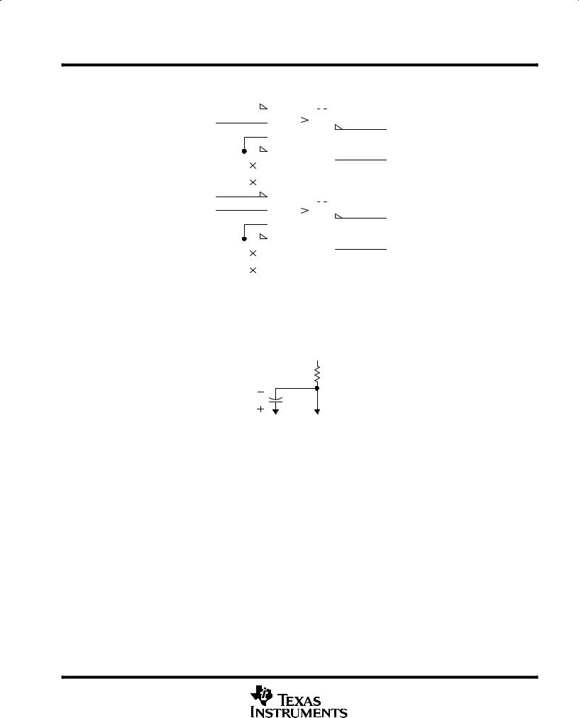
timing component connections
VCC
Rext
To Cext |
To Rext/Cext |
Terminal |
Terminal |
NOTE: Due to the internal circuit, the Rext/Cext terminal is never more positive than the Cext terminal.
POST OFFICE BOX 655303 •DALLAS, TEXAS 75265 |
3 |

SN54221, SN54LS221, SN74221, SN74LS221
DUAL MONOSTABLE MULTIVIBRATORS
WITH SCHMITT-TRIGGER INPUTS
SDLS213A ± DECEMBER 1983 ± REVISED FEBRUARY 1998
schematics of inputs and outputs
|
SN54/74221 |
EQUIVALENT OF EACH INPUT |
TYPICAL OF ALL OUTPUTS |
VCC |
VCC |
Req |
100 Ω NOM |
Input |
|
|
Output |
A Input: Req = 4 kΩ NOM |
|
B, CLR Input: Req = 2 kΩ NOM |
|
|
SN54/74LS221 |
EQUIVALENT OF EACH INPUT |
TYPICAL OF ALL OUTPUTS |
VCC |
VCC |
Req |
120 Ω NOM |
Input |
|
Output
A Input: Req = 25 kΩ NOM
B Input: Req = 15.4 kΩ NOM
CLR: Req = 12.5 kΩ NOM
4 |
POST OFFICE BOX 655303 •DALLAS, TEXAS 75265 |
SN54221, SN54LS221, SN74221, SN74LS221
DUAL MONOSTABLE MULTIVIBRATORS
WITH SCHMITT-TRIGGER INPUTS
SDLS213A ± DECEMBER 1983 ± REVISED FEBRUARY 1998
absolute maximum ratings over operating free-air temperature range (unless otherwise noted)²
Supply voltage range, VCC . . . . . . . . . . . . . . . . . . . . . . . . . . . . . . . . . . . . . . . . . . . . . . . . . . . . . . . . . |
. . . . . . . . . . 7 |
V |
Input voltage range, VI (see Note 1): 'LS221 . . . . . . . . . . . . . . . . . . . . . . . . . . . . . . . . . . . . . . . . . |
. . . . . . . . . . 7 |
V |
'221 . . . . . . . . . . . . . . . . . . . . . . . . . . . . . . . . . . . . . . . . . . . . |
. . . . . . . . 5.5 |
V |
Package thermal impedance, θJA (see Note 2): D package . . . . . . . . . . . . . . . . . . . . . . . . . . . . . |
. . . . . 113°C/W |
|
DB package . . . . . . . . . . . . . . . . . . . . . . . . . . . |
. . . . . 131°C/W |
|
N package . . . . . . . . . . . . . . . . . . . . . . . . . . . . . |
. . . . . . 78°C/W |
|
Storage temperature range, Tstg . . . . . . . . . . . . . . . . . . . . . . . . . . . . . . . . . . . . . . . . . . . . . . . . . . . |
±65°C to 150°C |
|
²Stresses beyond those listed under ªabsolute maximum ratingsº may cause permanent damage to the device. These are stress ratings only, and functional operation of the device at these or any other conditions beyond those indicated under ªrecommended operating conditionsº is not
implied. Exposure to absolute-maximum-rated conditions for extended periods may affect device reliability.
NOTES: 1. The input and output negative-voltage ratings may be exceeded if the input and output clamp-current ratings are observed.
2.The package thermal impedance is calculated in accordance with JESD 51, except for through-hole packages, which use a trace length of zero
recommended operating conditions
|
|
|
|
SN54221 |
|
|
SN74221 |
|
UNIT |
|
|
|
|
|
|
|
|
|
|
|
|
|
MIN |
NOM |
MAX |
MIN |
NOM |
MAX |
|
|
|
|
|
||||||
|
|
|
|
|
|
|
|
|
|
VCC |
Supply voltage |
|
4.5 |
5 |
5.5 |
4.75 |
5 |
5.25 |
V |
VIH |
High-level input voltage |
A input |
2 |
|
|
2 |
|
|
V |
VIL |
Low-level input voltage |
A input |
|
|
0.8 |
|
|
0.8 |
V |
IOH |
High-level output current |
|
|
|
±800 |
|
|
±800 |
A |
IOL |
Low-level output current |
|
|
|
16 |
|
|
16 |
mA |
v/ t |
Rise or fall of input pulse rate |
B input |
1* |
|
|
1 |
|
|
V/s |
|
|
|
|
|
|
|
|
||
A input |
1* |
|
|
1 |
|
|
V/ s |
||
|
|
|
|
|
|
||||
|
|
|
|
|
|
|
|
|
|
TA |
Operating free-air temperature |
|
±55 |
|
125 |
0 |
|
70 |
°C |
On products compliant to MIL-PRF-38535, this parameter is not production tested.
POST OFFICE BOX 655303 •DALLAS, TEXAS 75265 |
5 |
 Loading...