


 Loading...
ST STM32F051K4, STM32F051C4, STM32F051R4, STM32F051K6, STM32F051C6 User Manual
...STM32F051x4 STM32F051x6
STM32F051x8
Lowand medium-density advanced ARM™-based 32-bit MCU with 16 to 64 Kbytes Flash, timers, ADC, DAC and comm. interfaces
Features
■Operating conditions:
–Voltage range: 2.0 V to 3.6 V
■ARM 32-bit Cortex®-M0 CPU (48 MHz max)
■Memories
–16 to 64 Kbytes of Flash memory
–8 Kbytes of SRAM with HW parity checking
■CRC calculation unit
■Clock management
–4 to 32 MHz crystal oscillator
–32 kHz oscillator for RTC with calibration
–Internal 8 MHz RC with x6 PLL option
–Internal 40 kHz RC oscillator
■Calendar RTC with alarm and periodic wakeup from Stop/Standby
■Reset and supply management
–Power-on/Power down reset (POR/PDR)
–Programmable voltage detector (PVD)
■Low power Sleep, Stop, and Standby modes
■VBAT supply for RTC and backup registers
■5-channel DMA controller
■1 × 12-bit, 1.0 µs ADC (up to 16 channels)
–Conversion range: 0 to 3.6V
–Separate analog supply from 2.4 up to 3.6
■Two fast low-power analog comparators with programmable input and output
■One 12-bit D/A converter
■Up to 55 fast I/Os
–All mappable on external interrupt vectors
–Up to 36 I/Os with 5 V tolerant capability
■Up to 18 capacitive sensing channels supporting touchkey, linear and rotary touch sensors
■96-bit unique ID
■Serial wire debug (SWD)
LQFP64 10x10 |
LQFP48 7x7 |
UFQFPN32 5x5 |
|
|
|
■Up to 11 timers
–One 16-bit 7-channel advanced-control timer for 6 channels PWM output, with deadtime generation and emergency stop
–One 32-bit and one 16-bit timer, with up to 4 IC/OC, usable for IR control decoding
–One 16-bit timer, with 2 IC/OC, 1 OCN, deadtime generation and emergency stop
–Two 16-bit timers, each with IC/OC and OCN, deadtime generation, emergency stop and modulator gate for IR control
–One 16-bit timer with 1 IC/OC
–Independent and system watchdog timers
–SysTick timer: 24-bit downcounter
–One 16-bit basic timer to drive the DAC
■Communication interfaces
–Up to two I2C interfaces; one supporting Fast Mode Plus (1 Mbit/s) with 20 mA current sink, SMBus/PMBus, and wakeup from STOP
–Up to two USARTs supporting master synchronous SPI and modem control; one with ISO7816 interface, LIN, IrDA capability, auto baud rate detection and wakeup feature
–Up to two SPIs (18 Mbit/s) with 4 to 16 programmable bit frame, 1 with I2S interface multiplexed
–HDMI CEC interface, wakeup on header reception
Table 1. |
Device summary |
Reference |
Part number |
|
|
STM32F051x4 |
STM32F051K4, STM32F051C4, STM32F051R4 |
|
|
STM32F051x6 |
STM32F051K6, STM32F051C6, STM32F051R6 |
|
|
STM32F051x8 |
STM32F051C8, STM32F051R8, STM32F051K8 |
|
|
February 2012 |
Doc ID 018746 Rev 2 |
1/1 |
www.st.com

Contents |
STM32F051x |
|
|
Contents
1 |
Description . . . . . . . . . . . . . . . . . . . . . . . . . . . . . . . . . . . . . . . . . . . . . . . . |
. 6 |
|
2 |
Device overview . . . . . . . . . . . . . . . . . . . . . . . . . . . . . . . . . . . . . . . . . . . . |
8 |
|
3 |
Functional overview . . . . . . . . . . . . . . . . . . . . . . . . . . . . . . . . . . . . . . . . |
10 |
|
|
3.1 |
ARM® CortexTM-M0 core with embedded Flash and SRAM . . . . . . . . . |
10 |
|
3.2 |
Memories . . . . . . . . . . . . . . . . . . . . . . . . . . . . . . . . . . . . . . . . . . . . . . . . . |
10 |
|
3.3 |
Cyclic redundancy check calculation unit (CRC) . . . . . . . . . . . . . . . . . . . |
10 |
|
3.4 |
Direct memory access controller (DMA) . . . . . . . . . . . . . . . . . . . . . . . . . |
11 |
|
3.5 |
Nested vectored interrupt controller (NVIC) . . . . . . . . . . . . . . . . . . . . . . . |
11 |
|
3.6 |
Extended interrupt/event controller (EXTI) . . . . . . . . . . . . . . . . . . . . . . . . |
11 |
|
3.7 |
Clocks and startup . . . . . . . . . . . . . . . . . . . . . . . . . . . . . . . . . . . . . . . . . . |
12 |
|
3.8 |
Boot modes . . . . . . . . . . . . . . . . . . . . . . . . . . . . . . . . . . . . . . . . . . . . . . . |
12 |
|
3.9 |
Power management . . . . . . . . . . . . . . . . . . . . . . . . . . . . . . . . . . . . . . . . . |
12 |
3.9.1 Power supply schemes . . . . . . . . . . . . . . . . . . . . . . . . . . . . . . . . . . . . . 12 3.9.2 Power supply supervisors . . . . . . . . . . . . . . . . . . . . . . . . . . . . . . . . . . . 12 3.9.3 Voltage regulator . . . . . . . . . . . . . . . . . . . . . . . . . . . . . . . . . . . . . . . . . . 13
3.10 Low-power modes . . . . . . . . . . . . . . . . . . . . . . . . . . . . . . . . . . . . . . . . . . 13 3.11 Real-time clock (RTC) and backup registers . . . . . . . . . . . . . . . . . . . . . . 14 3.12 Timers and watchdogs . . . . . . . . . . . . . . . . . . . . . . . . . . . . . . . . . . . . . . . 15
3.12.1 Advanced-control timer (TIM1) . . . . . . . . . . . . . . . . . . . . . . . . . . . . . . . 15 3.12.2 General-purpose timers (TIM2..3, TIM14..17) . . . . . . . . . . . . . . . . . . . . 16 3.12.3 Basic timer TIM6 . . . . . . . . . . . . . . . . . . . . . . . . . . . . . . . . . . . . . . . . . . 16 3.12.4 Independent window watchdog (IWWDG) . . . . . . . . . . . . . . . . . . . . . . . 17 3.12.5 System window watchdog (WWDG) . . . . . . . . . . . . . . . . . . . . . . . . . . . 17 3.12.6 SysTick timer . . . . . . . . . . . . . . . . . . . . . . . . . . . . . . . . . . . . . . . . . . . . . 17
3.13 Inter-integrated circuit interfaces (I2C) . . . . . . . . . . . . . . . . . . . . . . . . . . . 17 3.14 Universal synchronous/asynchronous receiver transmitters (USART) . . . 18
3.15Serial peripheral interface (SPI)/Inter-integrated sound interfaces (I2S) . 19
3.16High-definition multimedia interface (HDMI) - consumer electronics control (CEC) 20
3.17 General-purpose inputs/outputs (GPIOs) . . . . . . . . . . . . . . . . . . . . . . . . . 20 3.18 Touch sensing controller (TSC) . . . . . . . . . . . . . . . . . . . . . . . . . . . . . . . . 20
2/3 |
Doc ID 018746 Rev 2 |

STM32F051x |
Contents |
|
|
3.19 Analog to digital converter (ADC) . . . . . . . . . . . . . . . . . . . . . . . . . . . . . . . 21
3.19.1 Temperature sensor . . . . . . . . . . . . . . . . . . . . . . . . . . . . . . . . . . . . . . . . 21
3.19.2 VBAT battery voltage monitoring . . . . . . . . . . . . . . . . . . . . . . . . . . . . . . . 21
|
3.20 |
Digital-to-analog converter (DAC) . . . . . . . . . . . . . . . . . . . . . . . . . . . . . . |
22 |
|
3.21 |
Fast low power comparators and reference voltage . . . . . . . . . . . . . . . . . |
22 |
|
|
3.21.1 Serial wire debug port (SW-DP) . . . . . . . . . . . . . . . . . . . . . . . . . . . . . . |
22 |
4 |
Pinouts and pin description . . . . . . . . . . . . . . . . . . . . . . . . . . . . . . . . . . |
23 |
|
5 |
Memory mapping . . . . . . . . . . . . . . . . . . . . . . . . . . . . . . . . . . . . . . . . . . |
31 |
|
6 |
Package characteristics . . . . . . . . . . . . . . . . . . . . . . . . . . . . . . . . . . . . . |
34 |
|
|
6.1 |
Package mechanical data . . . . . . . . . . . . . . . . . . . . . . . . . . . . . . . . . . . . |
34 |
7 |
Ordering information scheme . . . . . . . . . . . . . . . . . . . . . . . . . . . . . . . . |
38 |
|
8 |
Revision history . . . . . . . . . . . . . . . . . . . . . . . . . . . . . . . . . . . . . . . . . . . |
39 |
|
Doc ID 018746 Rev 2 |
3/3 |

List of tables |
STM32F051x |
|
|
List of tables
Table 1. Device summary . . . . . . . . . . . . . . . . . . . . . . . . . . . . . . . . . . . . . . . . . . . . . . . . . . . . . . . . . . 1 Table 2. STM32F051xx family device features and peripheral counts . . . . . . . . . . . . . . . . . . . . . . . . 7 Table 3. Timer feature comparison . . . . . . . . . . . . . . . . . . . . . . . . . . . . . . . . . . . . . . . . . . . . . . . . . . 15
Table 4. Comparison of I2C analog and digital filters . . . . . . . . . . . . . . . . . . . . . . . . . . . . . . . . . . . . 17 Table 5. STM32F051xx I2C implementation . . . . . . . . . . . . . . . . . . . . . . . . . . . . . . . . . . . . . . . . . . . 18
Table 6. STM32F051xx USART implementation . . . . . . . . . . . . . . . . . . . . . . . . . . . . . . . . . . . . . . . 19 Table 7. STM32F051x SPI/I2S implementation . . . . . . . . . . . . . . . . . . . . . . . . . . . . . . . . . . . . . . . . 19 Table 8. Capacitive sensing GPIOs available on STM32F051x devices . . . . . . . . . . . . . . . . . . . . . 20 Table 9. No. of capacitive sensing channels available on STM32F051xx devices. . . . . . . . . . . . . . 21 Table 10. Legend/abbreviations used in the pinout table . . . . . . . . . . . . . . . . . . . . . . . . . . . . . . . . . . 25 Table 11. Pin definitions . . . . . . . . . . . . . . . . . . . . . . . . . . . . . . . . . . . . . . . . . . . . . . . . . . . . . . . . . . . 25 Table 12. Alternate functions selected through GPIOA_AFR registers for port A . . . . . . . . . . . . . . . 29 Table 13. Alternate functions selected through GPIOB_AFR registers for port B . . . . . . . . . . . . . . . 30 Table 14. STM32F051x peripheral register boundary addresses. . . . . . . . . . . . . . . . . . . . . . . . . . . . 32 Table 15. LQFP64 – 10 x 10 mm 64 pin low-profile quad flat package mechanical data . . . . . . . . . . 35 Table 16. LQFP48 – 7 x 7mm, 48-pin low-profile quad flat package mechanical data. . . . . . . . . . . . 36 Table 17. UFQFPN32 - 32-lead ultra thin fine pitch quad flat no-lead package (5 x 5),
package mechanical data . . . . . . . . . . . . . . . . . . . . . . . . . . . . . . . . . . . . . . . . . . . . . . . . . 37 Table 18. Document revision history . . . . . . . . . . . . . . . . . . . . . . . . . . . . . . . . . . . . . . . . . . . . . . . . . 39
4/4 |
Doc ID 018746 Rev 2 |

STM32F051x |
List of figures |
|
|
List of figures
Figure 1. Block diagram . . . . . . . . . . . . . . . . . . . . . . . . . . . . . . . . . . . . . . . . . . . . . . . . . . . . . . . . . . . . 8 Figure 2. Clock tree . . . . . . . . . . . . . . . . . . . . . . . . . . . . . . . . . . . . . . . . . . . . . . . . . . . . . . . . . . . . . . . 9 Figure 3. LQFP64 64-pin package pinout . . . . . . . . . . . . . . . . . . . . . . . . . . . . . . . . . . . . . . . . . . . . . 23 Figure 4. LQFP48 48-pin package pinout . . . . . . . . . . . . . . . . . . . . . . . . . . . . . . . . . . . . . . . . . . . . . 24 Figure 5. UFQFPN32 32-pin package pinout. . . . . . . . . . . . . . . . . . . . . . . . . . . . . . . . . . . . . . . . . . . 24 Figure 6. STM32F051x memory map . . . . . . . . . . . . . . . . . . . . . . . . . . . . . . . . . . . . . . . . . . . . . . . . 31
Figure 7. LQFP64 – 10 x 10 mm 64 pin low-profile quad flat package outline . . . . . . . . . . . . . . . . . 35 Figure 8. Recommended footprint(1) . . . . . . . . . . . . . . . . . . . . . . . . . . . . . . . . . . . . . . . . . . . . . . . . . 35
Figure 9. LQFP48 – 7 x 7mm, 48-pin low-profile quad flat
package outline. . . . . . . . . . . . . . . . . . . . . . . . . . . . . . . . . . . . . . . . . . . . . . . . . . . . . . . . . . 36 Figure 10. Recommended footprint(1) . . . . . . . . . . . . . . . . . . . . . . . . . . . . . . . . . . . . . . . . . . . . . . . . . 36
Figure 11. UFQFPN32 - 32-lead ultra thin fine pitch quad flat no-lead package outline (5 x 5). . . . . . 37 Figure 12. UFQFPN32 recommended footprint(1) . . . . . . . . . . . . . . . . . . . . . . . . . . . . . . . . . . . . . . . . 37
Doc ID 018746 Rev 2 |
5/5 |

Description |
STM32F051x |
|
|
1 Description
The STM32F051xx family incorporates the high-performance ARM Cortex™-M0 32-bit RISC core operating at a 48 MHz frequency, high-speed embedded memories (Flash memory up to 64 Kbytes and SRAM up to 8 Kbytes), and an extensive range of enhanced peripherals and I/Os. All devices offer standard communication interfaces (up to two I2Cs, two SPIs, one I2S, one HDMI CEC, and up to two USARTs), one 12-bit ADC, one 12-bit DAC, up to five general-purpose 16-bit timers, a 32-bit timer and an advanced-control PWM timer.
The STM32F051xx family operates in the -40 to +85 °C and -40 to +105 °C temperature ranges, from a 2.0 to 3.6 V power supply. A comprehensive set of power-saving modes allows the design of low-power applications.
The STM32F051xx family includes devices in three different packages ranging from 32 pins to 64 pins. Depending on the device chosen, different sets of peripherals are included. The description below provides an overview of the complete range of peripherals proposed in this family.
These features make the STM32F051xx microcontroller family suitable for a wide range of applications such as application control and user interfaces, handheld equipment, A/V receivers and digital TV, PC peripherals, gaming and GPS platforms, industrial applications, PLCs, inverters, printers, scanners, alarm systems, video intercoms, and HVACs.
6/9 |
Doc ID 018746 Rev 2 |

STM32F051x |
|
|
|
|
|
|
|
|
|
|
|
|
|
|
Description |
|||
|
|
|
|
|
|
|
|
|
|
|
|
|
||||||
Table 2. |
STM32F051xx family device features and peripheral counts |
|
|
|
|
|
||||||||||||
|
|
|
|
|
|
|
|
|
|
|
|
|
|
|
|
|||
Peripheral |
|
|
STM32F051Kx |
|
|
STM32F051Cx |
|
STM32F051Rx |
||||||||||
|
|
|
|
|
|
|
|
|
|
|
|
|
|
|
|
|||
Flash (Kbytes) |
16 |
|
32 |
|
64 |
|
16 |
|
32 |
|
64 |
16 |
|
32 |
|
64 |
||
|
|
|
|
|
|
|
|
|
|
|
|
|
|
|
|
|
|
|
SRAM (Kbytes) |
|
|
4 |
|
8 |
|
|
4 |
|
8 |
|
4 |
|
8 |
||||
|
|
|
|
|
|
|
|
|
|
|
|
|
|
|
|
|
|
|
|
Advanced |
|
|
|
|
|
|
|
|
|
1 (16-bit) |
|
|
|
|
|
||
|
control |
|
|
|
|
|
|
|
|
|
|
|
|
|
|
|||
|
|
|
|
|
|
|
|
|
|
|
|
|
|
|
|
|
|
|
|
|
|
|
|
|
|
|
|
|
|
|
|
|
|
|
|
||
Timers |
General |
|
|
|
|
|
|
|
|
|
5 (16-bit) |
|
|
|
|
|
||
|
purpose |
|
|
|
|
|
|
|
|
|
1 (32-bit) |
|
|
|
|
|
||
|
|
|
|
|
|
|
|
|
|
|
|
|
|
|
|
|
||
|
Basic |
|
|
|
|
|
|
|
|
|
1 (16-bit) |
|
|
|
|
|
||
|
|
|
|
|
|
|
|
|
|
|
|
|
|
|
|
|
||
|
SPI (I2S)(1) |
|
|
1(1) (2) |
|
2(1) |
|
|
1(1) (2) |
|
2(1) |
|
1(1) (2) |
|
2(1) |
|||
Comm. |
I2C |
|
|
1(3) |
|
2 |
|
|
1(3) |
|
2 |
|
1(3) |
|
2 |
|||
|
|
|
|
|
|
|
|
|
|
|
|
|
|
|
|
|
|
|
interfaces |
USART |
1 |
(4) |
|
2 |
|
(4) |
|
2 |
(4) |
|
2 |
||||||
|
|
|
|
|
1 |
|
|
1 |
|
|
||||||||
|
CEC |
|
|
|
|
|
|
|
|
1 |
|
|
|
|
|
|
|
|
|
|
|
|
|
|
|
|
|
|
|
|
|
|
|
|
|
|
|
12-bit synchronized |
|
|
|
|
1 |
|
|
|
|
|
|
1 |
|
|
||||
ADC |
|
|
|
|
|
|
|
|
|
|
|
|
|
|||||
|
|
|
|
|
|
(10 ext. + 3 int.) |
|
|
|
(16 ext. + 3 int.) |
||||||||
(number of channels) |
|
|
|
|
|
|
|
|
||||||||||
|
|
|
|
|
|
|
|
|
|
|
|
|
|
|
|
|
||
|
|
|
|
|
|
|
|
|
|
|
|
|
|
|
|
|
|
|
GPIOs |
|
|
|
27 |
|
|
|
|
39 |
|
|
|
55 |
|
|
|||
|
|
|
|
|
|
|
|
|
|
|
|
|
|
|
|
|
|
|
Capacitive sensing |
|
|
14 |
|
|
|
|
17 |
|
|
|
18 |
|
|
||||
channels |
|
|
|
|
|
|
|
|
|
|
|
|
||||||
|
|
|
|
|
|
|
|
|
|
|
|
|
|
|
|
|
|
|
|
|
|
|
|
|
|
|
|
|
|
|
|
|
|
|
|
|
|
12-bit DAC |
|
|
|
|
|
|
|
|
|
1 |
|
|
|
|
|
|
|
|
(number of channels) |
|
|
|
|
|
|
|
|
(1) |
|
|
|
|
|
|
|
||
|
|
|
|
|
|
|
|
|
|
|
|
|
|
|
|
|
||
Analog comparator |
|
|
|
|
|
|
|
|
2 |
|
|
|
|
|
|
|
||
|
|
|
|
|
|
|
|
|
|
|
|
|
|
|
|
|
|
|
Max. CPU frequency |
|
|
|
|
|
|
|
|
|
48 MHz |
|
|
|
|
|
|
|
|
|
|
|
|
|
|
|
|
|
|
|
|
|
|
|
||||
Operating voltage |
|
|
|
|
|
|
|
|
2.0 to 3.6 V |
|
|
|
|
|
||||
|
|
|
|
|
|
|
|
|||||||||||
Operating temperature |
|
|
|
Ambient operating temperature: -40 °C to 85 °C / -40 °C to 105 °C |
|
|
||||||||||||
|
|
|
|
|
Junction temperature: -40 °C to 125 °C |
|
|
|
|
|||||||||
|
|
|
|
|
|
|
|
|
|
|
||||||||
|
|
|
|
|
|
|
|
|
|
|
|
|
|
|
||||
Packages |
|
|
|
UFQFPN32 |
|
|
|
LQFP48 |
|
|
|
|
LQFP64 |
|
|
|||
|
|
|
|
|
|
|
|
|
|
|
|
|
|
|
|
|
|
|
1.The SPI1 interface can be used either in SPI mode or in I2S audio mode.
2.SPI2 is not present
3.I2C2 is not present
4.USART2 is not present
Doc ID 018746 Rev 2 |
7/9 |

Device overview |
STM32F051x |
|
|
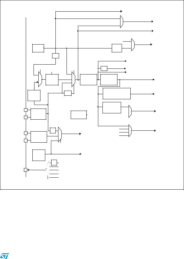
2 Device overview
Figure 1. Block diagram
37#,+ |
3ERIALA7IRE |
|
|
|
|
6$$ |
|
0/7%2 |
6$$ TO 6 6 |
|
37$!4 |
$EBUG |
|
|
|
|
|
|
6/,4 2%' |
||
AS !& |
|
|
|
|
|
|
|
|
||
|
OBL |
|
&,!3( |
|
|
6 4/ 6 |
633 |
|||
|
|
)NTERFACE |
|
|
||||||
|
|
FLASH |
+" |
|
|
|
6$$ |
|
|
|
|
#/24%8 - #05 |
BITS |
|
|
|
|
|
|||
|
|
|
|
|
|
|
||||
|
F(#,+ -(Z |
|
|
0/2 |
|
3500,9 |
|
|||
|
|
|
|
|
|
.234 |
||||
|
|
|
CONTROLLER |
|
|
2ESET |
350%26)3)/. |
|||
|
|
|
32!- |
|
|
|
|
6$$! |
||
|
.6)# |
32!- |
6$$! |
)NT |
|
0/2 0$2 |
||||
|
+" |
|
6$$ |
|||||||
|
|
|
|
|||||||
|
.6)# |
|
|
|
|
|
||||
|
|
2# (3 -(Z |
|
|
|
06$ |
|
|||
|
ATRIX- |
|
|
|
|
|
||||
|
|
|
|
|
|
|
|
|||
|
"US |
|
|
|
2# (3 (-(Z |
|
6$$! |
6$$ |
|
|
|
'0 $-! |
|
|
|
2# ,3 |
|
|
|
/3#). 0& |
|
|
CHANNELS |
|
|
|
|
|
|
|
||
|
|
|
|
0,, |
|
|
|
84!, /3# |
||
|
|
|
|
|
|
|
|
-(Z |
/3#/54 0& |
|
|
|
|
|
|
|
|
|
|
|
|
|
|
|
|
|
|
|
|
)77$' |
|
|
|
|
|
|
|
!("0#,+ |
|
|
0OWER |
|
|
|
|
|
|
2%3%4 |
!0"0#,+ |
|
|
#ONTROLLER |
6"!4 6 TO 6 |
|
|
|
|
|
!$##,+ |
|
|
|
|
|
|
|
|
|
|
#,/#+ |
#%##,+ |
|
|
|
637 |
|
|
|
|
|
#/.42/, |
53!24#,+ |
|
|
84!, K(Z |
/3# ?). |
|
0!; = |
'0)/ PORTT! |
|
|
|
(#,+ |
|
|
/3# ?/54 |
||
|
|
|
|
|
|
|
||||
|
|
|
|
|
,+ |
|
|
|
|
|
0"; = |
'0)/ PORTT" |
DECODER |
|
|
|
|
24# |
"ACKUP |
4!-0%2 24# |
|
|
|
|
|
REG |
||||||
|
|
|
|
|
|
|
|
!,!2- /54 |
||
|
|
|
|
|
|
|
|
|
||
0#; = |
'0)/ PORTT# |
|
#2# |
|
|
24# INTERFACE |
|
|||
|
|
!(" |
|
|
|
|
|
|
|
|
0$ |
'0)/ PORTT$ |
|
|
|
|
|
4)-%2- |
CHANNELS |
||
|
|
|
|
|
COMPL CHANNELS |
|||||
|
|
|
|
|
|
|||||
|
|
|
|
|
|
|
|
|||
0&; = |
'0)/ PORTT& |
|
|
|
|
|
|
|
|
"2+ %42 INPUT AS !& |
|
|
|
|
|
|
4)-%2- |
CH %42 AS !& |
|||
|
|
|
|
|
|
|
|
|||
GROUPS OF |
!NALOG |
|
|
|
|
|
|
4)-%2- |
CH %42 AS !& |
|
CHANNELS |
SWITCHES 4OUCH 3ENSING |
|
|
|
|
|
|
|
|
|
|
#ONTROLLER |
|
|
|
|
|
|
4)-%2- |
CHANNEL AS !& |
|
39.# |
|
!(" |
|
|
|
|
|
|||
|
|
|
|
|
|
|
|
|
||
|
|
!0" |
|
|
|
|
|
4)-%2- |
CHANNELS |
|
|
|
|
|
|
|
|
COMPL "2+ AS !& |
|||
|
|
|
|
|
|
|
|
|
|
|
|
|
|
|
|
|
|
|
4)-%2- |
CHANNEL |
|
|
|
|
|
|
|
|
|
COMPL "2+ AS !& |
||
|
%84 )4 |
|
|
|
|
|
|
|
|
|
!& |
|
|
|
|
|
|
|
|
CHANNEL |
|
7+50 |
|
|
77$' |
|
|
4)-%2- |
||||
|
|
|
|
|
COMPL "2+ AS !& |
|||||
|
|
|
|
|
|
|
|
|||
-/3) 3$ |
|
|
|
|
|
|
|
|
|
)2?/54 AS5!& |
-)3/ -#+ |
|
|
|
|
|
|
|
|
|
|
30) ) 3 |
|
|
|
|
|
|
|
|
|
|
3#+ #+ |
|
|
|
|
|
|
|
|
|
|
|
|
|
$"'-#5 |
|
|
|
|
28 48 #43 243 |
||
.33 73 AS7!& |
|
|
|
|
|
53!24 |
||||
|
|
|
|
|
|
|
|
#+ AS !& |
||
-/3) -)3/ |
|
|
|
|
|
|
|
|
|
|
30) |
|
|
|
|
|
|
|
|
|
|
3#+ .33 |
|
|
|
|
|
|
53!24 |
28 48 #43 243 |
||
AS !& |
|
|
|
|
|
|
|
|
|
#+ AS !& |
|
393#&' )& |
|
|
|
|
|
|
) # |
3#, 3$! 3-"AL |
|
|
|
|
|
|
|
|
|
M! FOR &- |
||
|
|
|
|
|
|
|
|
|
|
AS !& |
|
|
|
|
|
|
|
|
) # |
3#, 3$! |
|
).054 |
'0 #OMPARATOR |
|
|
|
|
|
|
|
|
AS !& |
).054 |
'0 #OMPARATOR |
|
|
|
|
|
|
|
|
|
/54054 |
|
|
|
|
|
|
|
|
|
|
ASA!& |
|
|
|
|
|
|
|
|
|
|
|
6$$! |
|
|
|
|
|
|
($-) #%# |
#%# AS !& |
|
|
4EMP SENSOR |
|
|
|
|
|
|
|
|
|
|
BIT !$# )& |
|
|
|
|
|
|
|
|
|
!$ INPUTS |
|
|
|
|
|
|
|
|
|
|
|
|
|
|
|
|
|
|
|
|
|
|
|
|
|
|
|
|
)& |
BIT $!# |
|
|
|
|
|
|
4)-%2 |
|
)& |
|
|
$!# ?/54 AS !& |
|
|
|
|
|
|
|
|
|
|
|
|
6$$! |
|
|
|
|
|
|
|
|
|
|
633! |
6$$! |
|
|
|
|
|
|
|
6$$! |
|
|
|
|
|
|
|
|
|
|
||
|
|
|
|
|
|
|
|
|
|
-3 6 |
8/9 |
Doc ID 018746 Rev 2 |
STM32F051x |
Device overview |
|
|
Figure 2. Clock tree
/3#?/54 /3#?).
/3# ?). /3# ?/54
-#/
&,)4,+
TO &LASH PROGRAMMING INTERFACE
|
|
|
|
(3) |
|
|
|
|
|
|
393#,+ |
|
TO ) # |
|
|
|
|
|
|
|
|
|
|
|
|
|
TO ) 3 |
|
|
|
|
,3% |
|
|
-(Z (3) |
|
|
|
|
TO #%# |
|
(3)32# |
|
|
|
|
|
|
|
|
|
|
|
|
|
|
|
|
|
|
|
|
|
|
|
|
(#,+ |
TO !(" BUS CORE |
|
|
|
|
|
|
MEMORYYANDA$-! |
|
0,,32# |
37 |
|
|
TO CORTEXX3YSTEM TIMER |
||
0,,-5, |
(3) |
|
|
&(#,+##ORTEXXFREE RUNNING CLOCKK |
||
|
|
|
|
|||
|
0,, |
!(" |
!0" |
|
|
|
|
|
|
|
|||
|
0,,#,+ |
!(" |
|
0#,+ |
TO !0" PERIPHERALS |
|
|
X X |
PRESCALER |
PRESCALER |
|||
|
X |
(3% |
|
|
|
|
|
|
|
|
|
|
|
|
|
#33 |
393#,+ |
)F !0" PRESCALER |
TO 4)- |
|
|
|
|||||
|
|
X ELSE X |
||||
|
|
|
|
|
||
|
|
|
|
|
||
|
|
|
|
!$# |
|
|
|
|
|
|
0RESCALER |
|
|
-(Z |
|
-(Z (3) |
|
|
TO !$# |
|
|
|
|
-(Z MAX |
|||
(3%3/3# |
|
|
|
|||
|
(3) )2# |
|
|
|
||
|
|
|
|
0#,+ |
|
|
|
|
24##,+ |
|
393#,+ |
|
TO 53!24 |
,3%3/3# |
|
TO 24# |
(3) |
|
|
|
|
|
,3% |
|
|
||
|
|
|
|
|
||
K(Z |
,3% |
|
|
|
|
|
|
24#3%,; = |
|
|
|
|
|
,3)32# |
,3) |
|
TO )77$' |
|
|
|
|
|
)77$'#,+ |
|
|
|
|
K(Z |
|
|
|
|
|
|
|
|
|
|
|
|
|
-AIN CLOCK |
|
0,,#,+ |
|
|
|
|
|
(3) |
|
|
|
|
|
OUTPUT |
|
|
|
|
|
|
|
(3) |
|
|
|
|
|
|
|
|
|
|
|
|
|
|
(3% |
|
|
|
|
|
|
393#,+ |
|
|
|
|
-#/ |
|
|
|
|
|
|
|
|
|
|
|
|
-3 6 |
Doc ID 018746 Rev 2 |
9/9 |

Functional overview |
STM32F051x |
|
|
3 Functional overview
3.1ARM® CortexTM-M0 core with embedded Flash and SRAM
The ARM Cortex™-M0 processor is the latest generation of ARM processors for embedded systems. It has been developed to provide a low-cost platform that meets the needs of MCU implementation, with a reduced pin count and low-power consumption, while delivering outstanding computational performance and an advanced system response to interrupts.
The ARM Cortex™-M0 32-bit RISC processor features exceptional code-efficiency, delivering the high-performance expected from an ARM core in the memory size usually associated with 8- and 16-bit devices.
The STM32F051xx family has an embedded ARM core and is therefore compatible with all ARM tools and software.
Figure 1 shows the general block diagram of the device family.
3.2Memories
The device has the following features:
●Up to 8 Kbytes of embedded SRAM accessed (read/write) at CPU clock speed with 0 wait states and featuring embedded parity checking with exception generation for failcritical applications.
●The non-volatile memory is divided into two arrays:
–16 to 64 Kbytes of embedded Flash memory for programs and data
–Option bytes
The option bytes are used to write-protect the memory (with 4 KB granularity) and/or readout-protect the whole memory with the following options:
–Level 0: no readout protection
–Level 1: memory readout protection, the Flash memory cannot be read from or written to if either debug features are connected or boot in RAM is selected
–Level 2: chip readout protection, debug features (Cortex-M0 serial wire) and boot in RAM selection disabled
3.3Cyclic redundancy check calculation unit (CRC)
The CRC (cyclic redundancy check) calculation unit is used to get a CRC code from a 96-bit data word and a fixed generator polynomial.
Among other applications, CRC-based techniques are used to verify data transmission or storage integrity. In the scope of the EN/IEC 60335-1 standard, they offer a means of verifying the Flash memory integrity. The CRC calculation unit helps compute a signature of the software during runtime, to be compared with a reference signature generated at linktime and stored at a given memory location.
10/22 |
Doc ID 018746 Rev 2 |
STM32F051x |
Functional overview |
|
|
3.4Direct memory access controller (DMA)
The 5-channel general-purpose DMAs manage memory-to-memory, peripheral-to-memory and memory-to-peripheral transfers.
The DMA supports circular buffer management, removing the need for user code intervention when the controller reaches the end of the buffer.
Each channel is connected to dedicated hardware DMA requests, with support for software trigger on each channel. Configuration is made by software and transfer sizes between source and destination are independent.
DMA can be used with the main peripherals: SPI, I2S, I2C, USART, all TIMx timers (except TIM14), DAC and ADC.
3.5Nested vectored interrupt controller (NVIC)
The STM32F051xx family embeds a nested vectored interrupt controller able to handle up to 32 maskable interrupt channels (not including the 16 interrupt lines of Cortex™-M0) and 16 priority levels.
●Closely coupled NVIC gives low latency interrupt processing
●Interrupt entry vector table address passed directly to the core
●Closely coupled NVIC core interface
●Allows early processing of interrupts
●Processing of late arriving higher priority interrupts
●Support for tail-chaining
●Processor state automatically saved
●Interrupt entry restored on interrupt exit with no instruction overhead
This hardware block provides flexible interrupt management features with minimal interrupt latency.
3.6Extended interrupt/event controller (EXTI)
The external interrupt/event controller consists of 24 edge detector lines used to generate interrupt/event requests and wake-up the system. Each line can be independently configured to select the trigger event (rising edge, falling edge, both) and can be masked independently. A pending register maintains the status of the interrupt requests. The EXTI can detect an external line with a pulse width shorter than the internal clock period. Up to 55 GPIOs can be connected to the 16 external interrupt lines.
Doc ID 018746 Rev 2 |
11/22 |

Functional overview |
STM32F051x |
|
|
3.7Clocks and startup
System clock selection is performed on startup, however the internal RC 8 MHz oscillator is selected as default CPU clock on reset. An external 4-32 MHz clock can be selected, in which case it is monitored for failure. If failure is detected, the system automatically switches back to the internal RC oscillator. A software interrupt is generated if enabled. Similarly, full interrupt management of the PLL clock entry is available when necessary (for example on failure of an indirectly used external crystal, resonator or oscillator).
Several prescalers allow the application to configure the frequency of the AHB and the APB domains. The maximum frequency of the AHB and the APB domains is 48 MHz.
3.8Boot modes
At startup, the boot pin and boot selector option bit are used to select one of three boot options:
●Boot from User Flash
●Boot from System Memory
●Boot from embedded SRAM
The boot loader is located in System Memory. It is used to reprogram the Flash memory by using USART1.
3.9Power management
3.9.1Power supply schemes
●VDD = 2.0 to 3.6 V: external power supply for I/Os and the internal regulator. Provided externally through VDD pins.
●VDDA = 2.0 to 3.6 V: external analog power supply for ADC, Reset blocks, RCs and PLL (minimum voltage to be applied to VDDA is 2.4 V when the ADC and DAC are used). The VDDA voltage level must be always greater or equal to the VDD voltage level and must be provided first.
●VBAT = 1.6 to 3.6 V: power supply for RTC, external clock 32 kHz oscillator and backup registers (through power switch) when VDD is not present.
For more details on how to connect power pins, refer to Figure 9: Power supply scheme.
3.9.2Power supply supervisors
The device has integrated power-on reset (POR) and power-down reset (PDR) circuits. They are always active, and ensure proper operation above a threshold of 2 V. The device remains in reset mode when the monitored supply voltage is below a specified threshold, VPOR/PDR, without the need for an external reset circuit.
●The POR monitors only the VDD supply voltage. During the startup phase it is required that VDDA should arrive first and be greater than or equal to VDD.
●The PDR monitors both the VDD and VDDA supply voltages, however the VDDA power supply supervisor can be disabled (by programming a dedicated Option bit) to reduce
the power consumption if the application design ensures that VDDA is higher than or equal to VDD.
12/22 |
Doc ID 018746 Rev 2 |
Loading...