


 Loading...
LD39015Jxx
150 mA low quiescent current low noise voltage regulator
Features
■Input voltage from 1.5 to 5.5 V
■Ultra low dropout voltage (90 mV typ. at 100 mA load)
■Very low quiescent current (20 µA typ. at no load, 35 µA typ. at 150 mA load, 1 µA max in off mode)
■Low noise (54 µVRMS from 10 Hz to 100 kHz at VOUT = 1.8 V)
■Output voltage tolerance: ± 2.0% @ 25 °C
■150 mA guaranteed output current
■Wide range of output voltages available on request: 0.8 V to 4.5 V with 100 mV step
■Logic-controlled electronic shutdown
■Compatible with ceramic capacitor COUT = 1 µF
■Internal current and thermal limit
■Flip-chip 4 bumps 1.1 x 1.1 mm.
■Temperature range: -40 °C to 125 °C
Flip-chip 4
74 dB at low frequencies and starts to roll off at 10 kHz. Enable logic control function puts the LD39015Jxx in shut-down mode allowing a total current consumption lower than 1 µA. The device also includes a short-circuit constant current limiting and thermal protection. Typical applications are mobile phones, personal digital assistant (PDAs), cordless phone and similar battery powered systems.
Description
The LD39015Jxx provides 150 mA maximum current from an input voltage ranging from 1.5 V to 5.5 V with a typical dropout voltage of 80 mV. It is stable with ceramic capacitor. The ultra low drop-voltage, low quiescent current and low noise features make it suitable for low power battery powered applications. Power supply rejection is
Table 1. |
Device summary |
|
|
|
Part numbers |
Order codes |
Output voltages |
|
|
|
|
|
LD39015JXX12 |
LD39015J12R |
1.2 V |
|
|
|
|
|
LD39015JXX13 |
LD39015JJ13R |
1.3 V |
|
|
|
|
|
LD39015JXX15 |
LD39015J15R |
1.5 V |
|
|
|
|
|
LD39015JXX18 |
LD39015J18R |
1.8 V |
|
|
|
|
|
LD39015JXX28 |
LD39015J28R |
2.8 V |
|
|
|
|
August 2009 |
|
Doc ID 15968 Rev 2 |
1/17 |
|
|
|
|
|
|
|
www.st.com |

Contents |
LD39015Jxx |
|
|
Contents
1 |
Diagram . . . . . . . . . . . . . . . . . . . . . . . . . . . . . . . . . . . . . . . . . . . . . . . . . . |
. 3 |
2 |
Pin configuration . . . . . . . . . . . . . . . . . . . . . . . . . . . . . . . . . . . . . . . . . . |
. 4 |
3 |
Typical application . . . . . . . . . . . . . . . . . . . . . . . . . . . . . . . . . . . . . . . . . . |
5 |
4 |
Maximum ratings . . . . . . . . . . . . . . . . . . . . . . . . . . . . . . . . . . . . . . . . . . . . |
6 |
5 |
Electrical characteristics . . . . . . . . . . . . . . . . . . . . . . . . . . . . . . . . . . . . . |
7 |
6 |
Typical performance characteristics . . . . . . . . . . . . . . . . . . . . . . . . . . . . |
9 |
7 |
Package mechanical data . . . . . . . . . . . . . . . . . . . . . . . . . . . . . . . . . . . . |
11 |
8 |
Different output voltage versions of the LD39015Jxx |
|
|
available on request . . . . . . . . . . . . . . . . . . . . . . . . . . . . . . . . . . . . . . . . |
15 |
9 |
Revision history . . . . . . . . . . . . . . . . . . . . . . . . . . . . . . . . . . . . . . . . . . . |
16 |
2/17 |
Doc ID 15968 Rev 2 |

LD39015Jxx |
Diagram |
|
|
1 Diagram
Figure 1. Block diagram
IN |
OUT |
|
|
|
BandGap |
|
1.22 V |
|
R1 |
|
Trimming |
|
Thermal |
|
R2 |
|
Protection |
|
Enable |
EN |
|
|
GND |
Doc ID 15968 Rev 2 |
3/17 |
Pin configuration |
LD39015Jxx |
|
|
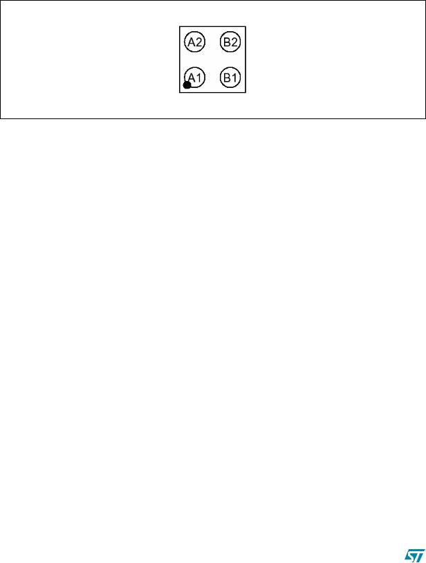
2 Pin configuration
Figure 2. Pin connection (top view)
Table 2. |
Pin description |
|
|
Pin n° |
|
Symbol |
Function |
|
|
|
|
A2 |
|
EN |
Enable pin logic input: Low=shutdown, High=active |
|
|
|
|
A1 |
|
GND |
Common ground |
|
|
|
|
B2 |
|
IN |
Input voltage of the LDO |
|
|
|
|
B1 |
|
OUT |
Output voltage |
|
|
|
|
4/17 |
Doc ID 15968 Rev 2 |
LD39015Jxx |
Typical application |
|
|
3 Typical application
Figure 3. Typical application circuit
VIN |
IN |
OUT |
|
VOUT |
1 µF |
|
|
1 µF |
Load |
VEN |
EN |
GND |
Doc ID 15968 Rev 2 |
5/17 |

Maximum ratings |
|
|
LD39015Jxx |
||||
|
|
|
|
|
|
|
|
4 |
Maximum ratings |
|
|
|
|
|
|
Table 3. |
Absolute maximum ratings |
|
|
|
|
|
|
|
|
|
|
|
|
|
|
Symbol |
|
Parameter |
|
Value |
|
|
Unit |
|
|
|
|
|
|
|
|
VIN |
|
DC input voltage |
|
- 0.3 to 6 |
|
|
V |
VOUT |
|
DC output voltage |
|
- 0.3 to VI + 0.3 |
|
|
V |
VEN |
|
Enable input voltage |
|
- 0.3 to VI + 0.3 |
|
|
V |
IOUT |
|
Output current |
|
Internally limited |
|
|
mA |
PD |
|
Power dissipation |
|
Internally limited |
|
|
mW |
TSTG |
|
Storage temperature range |
|
-65 to 150 |
|
|
°C |
TOP |
|
Operating junction temperature range |
|
-40 to 125 |
|
|
°C |
Note: |
Absolute maximum ratings are those values beyond which damage to the device may occur. |
||||||
|
Functional operation under these conditions is not implied. All values are referred to GND. |
||||||
Table 4. |
Thermal data |
|
|
|
|
|
|
|
|
|
|
|
|
|
|
Symbol |
|
Parameter |
|
Value |
|
|
Unit |
|
|
|
|
|
|
|
|
RthJA |
|
Thermal resistance junction-ambient |
|
180 |
|
|
°C/W |
6/17 |
Doc ID 15968 Rev 2 |
Loading...