


ST UC2842A, UC2843A, UC2844A, UC2845A, UC3842A User Manual
...
|
UC2842A/3A/4A/5A |
|
UC3842A/3A/4A/5A |
HIGH PERFORMANCE CURRENT MODE PWM CONTROLLER
.TRIMMED OSCILLATOR DISCHARGE CUR-
.RENT
.CURRENT MODE OPERATION TO 500kHz
AUTOMATIC FEED FORWARD COMPENSA-
.TION
LATCHING PWM FOR CYCLE-BY-CYCLE
.CURRENT LIMITING
INTERNALLY TRIMMED REFERENCE WITH
.UNDERVOLTAGE LOCKOUT
.HIGH CURRENT TOTEM POLE OUTPUT UNDERVOLTAGE LOCKOUT WITH HYSTER-
.ESIS
.LOW START-UP CURRENT (< 0.5mA) DOUBLE PULSE SUPPRESSION
DESCRIPTION
TheUC384xA family ofcontrolICsprovidesthenecessary features to implement off-line or DC to DC fixed frequencycurrent mode control schemes with a minimal external parts count. Internally implemented circuits include a trimmed oscillator for precise DUTY CYCLE CONTROL under voltage lock- outfeaturingstart-up current less than0.5mA,a precision reference trimmed for accuracy at the error amp input, logicto insure latched operation,a PWM
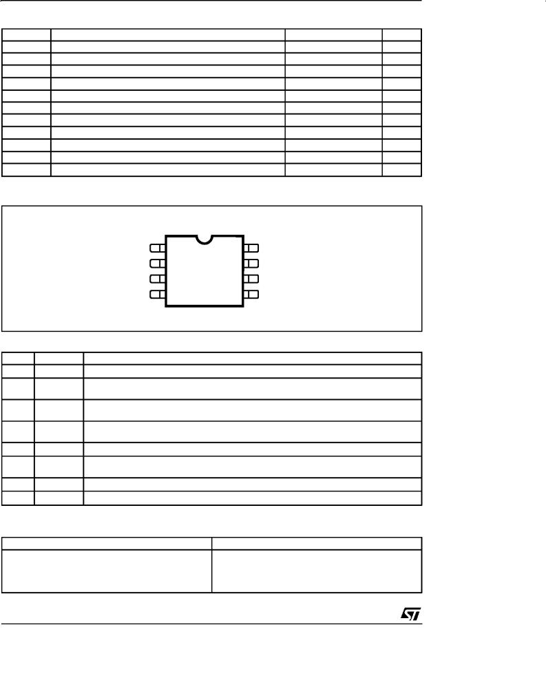
Mini dip |
SO8 |
comparatorwhich alsoprovidescurrent limit control, and a totem pole output stage designed to source or sink high peakcurrent. The outputstage, suitable for driving N-Channel MOSFETs, is low in the offstate.
Differences between members of this family are the under-voltagelockout thresholdsand maximum duty cycle ranges. The UC3842A and UC3844A have UVLO thresholds of 16V (on) and 10V (off), ideally suitedoff-lineapplicationsThecorrespondingthresh- olds for the UC3843A and UC3845A are 8.5 V and 7.9V. The UC3842A and UC3843A can operate to dutycycles approaching100%.A range of the zeroto < 50 % is obtainedby theUC3844Aand UC3845Aby theaddition of an internal toggle flip flopwhich blanks the output off every otherclock cycle.
BLOCK DIAGRAM (toggle flip flop used only in UC3844A and UC3845A)
7
Vi |
|
|
|
|
|
|
34V |
UVLO |
|
5V |
8 VREF |
|
|
|
|||
|
5 |
|
S/R |
||
GROUND |
|
REF |
5V 50mA |
||
|
|
|
|||
|
|
|
|
INTERNAL |
|
|
|
2.50V |
|
|
BIAS |
|
|
|
|
VREF GOOD |
|
|
|
|
|
LOGIC |
6 |
|
4 |
|
|
|
OUTPUT |
RT/CT |
OSC |
|
T |
|
|
|
|
|
|||
|
+ |
ERROR AMP. |
|
S |
|
|
2R |
|
|
||
VFB |
2 |
|
|
R |
PWM |
- |
R |
|
|||
|
1 |
|
1V |
LATCH |
|
|
|
|
|
||
COMP |
|
|
CURRENT |
|
|
|
|
|
|
||
|
3 |
|
|
SENSE |
UC3842A |
CURRENT |
|
|
COMPARATOR |
||
|
|
|
|||
SENSE
D95IN331
March 1999 |
1/15 |
UC2842A/3A/4A/5A - UC3842A/3A/4A/5A
ABSOLUTE MAXIMUM RATINGS
Symbol |
|
Parameter |
Valu e |
Un it |
|||
Vi |
Supply Voltage (low impedance source) |
30 |
V |
||||
Vi |
Supply Voltage (Ii < 30mA) |
|
|
Self Limiting |
|
||
IO |
Output Current |
|
|
|
±1 |
A |
|
EO |
Output Energy (capacitive load) |
5 |
μJ |
||||
|
|
Analog Inputs (pins 2, 3) |
|
|
|
± 0.3 to 5.5 |
V |
|
|
Error Amplifier Output Sink Current |
10 |
mA |
|||
P |
tot |
Power Dissipation at Tamb |
≤ |
25 |
° |
1.25 |
W |
|
|
C (Minidip) |
|
|
|||
Ptot |
Power Dissipation at Tamb ≤ 25 °C (SO8) |
800 |
mW |
||||
Tstg |
Storage Temperature Range |
|
± 65 to 150 |
°C |
|||
TJ |
Junction Operating Temperature |
± 40 to 150 |
°C |
||||
TL |
Lead Temperature (soldering 10s) |
300 |
°C |
||||
* All voltages are with respect to pin 5, all currents are positive into the specified terminal.
PIN CONNECTION (top view)
Minidip/SO8
COMP |
1 |
8 |
VREF |
VFB |
2 |
7 |
Vi |
ISENSE |
3 |
6 |
OUTPUT |
RT/CT |
4 |
5 |
GROUND |
|
|
D95IN332 |
|
PIN FUNCTIONS
No |
Function |
Description |
1 |
COMP |
This pin is the Error Amplifier output and is made available for loop compensation. |
2 |
VFB |
This is the inverting input of the Error Amplifier. It is normally connected to the switching |
|
|
power supply output through a resistor divider. |
3ISENSE
4RT/CT
A voltage proportional to inductor current is connected to this input. The PWM uses this information to terminate the output switch conduction.
The oscillator frequency and maximum Output duty cycle are programmed by connecting resistor RT to Vref and cpacitor CT to ground. Operation to 500kHz is possible.
5 |
GROUND |
This pin is the combined control circuitry and power ground. |
6 |
OUTPUT |
This output directly drives the gate of a power MOSFET. Peak currents up to 1A are sourced |
|
|
and sunk by this pin. |
7 |
VCC |
This pin is the positive supply of the control IC. |
8 |
Vref |
This is the reference output. It provides charging current for capacitor CT through resistor RT. |
ORDERING NUMBERS
SO8 |
Minidip |
UC2842AD1; UC3842AD1 |
UC2842AN; UC3842AN |
UC2843AD1; UC3843AD1 |
UC2843AN; UC3843AN |
UC2844AD1; UC3844AD1 |
UC2844AN; UC3844AN |
UC2845AD1; UC3845AD1 |
UC2845AN; UC3845AN |
2/15

UC2842A/3A/4A/5A - UC3842A/3A/4A/5A
THERMAL DATA
Symbo l |
Descri ption |
|
Minid ip |
SO 8 |
Unit |
Rth j-amb |
Thermal Resistance Junction-ambient. |
max. |
100 |
150 |
°C/W |
ELECTRICAL CHARACTERISTICS ( [note 1] Unless otherwise stated, these specifications apply for -25 < Tamb < 85°C for UC284XA; 0 < Tamb < 70°C for UC384XA; Vi = 15V (note 5); RT = 10K; CT = 3.3nF)
Symbo l |
Parameter |
T est Cond it ion s |
UC284XA |
UC384XA |
Uni t |
||||||||
Mi n. T yp. Max. Min. Typ . Max. |
|||||||||||||
|
|
|
|
|
|
|
|||||||
REFERENCE SECTION |
|
|
|
|
|
|
|
|
|
||||
VREF |
|
Output Voltage |
Tj = 25°C Io = 1mA |
4.95 |
5.00 |
5.05 |
4.90 |
5.00 |
5.10 |
V |
|||
VREF |
Line Regulation |
12V ≤ Vi ≤ 25V |
|
2 |
20 |
|
2 |
20 |
mV |
||||
VREF |
Load Regulation |
1 ≤ Io ≤ 20mA |
|
3 |
25 |
|
3 |
25 |
mV |
||||
VREF/ |
T |
Temperature Stability |
(Note 2) |
|
|
0.2 |
|
|
0.2 |
|
mV/°C |
||
|
|
|
Total Output Variation |
Line, Load, Temperature |
4.9 |
|
5.1 |
4.82 |
|
5.18 |
V |
||
|
eN |
|
Output Noise Voltage |
10Hz ≤ f ≤ 10KHz Tj = 25°C |
|
50 |
|
|
50 |
|
μV |
||
|
|
|
|
(note 2) |
|
|
|
|
|
|
|
|
|
|
|
|
Long Term Stability |
Tamb = 125°C, 1000Hrs |
|
5 |
25 |
|
5 |
25 |
mV |
||
|
|
|
|
(note 2) |
|
|
|
|
|
|
|
|
|
|
ISC |
|
Output Short Circuit |
|
|
-30 |
-100 |
-180 |
-30 |
-100 |
-180 |
mA |
|
OSCILLATOR SECTION |
|
|
|
|
|
|
|
|
|
||||
f |
OSC |
|
Frequency |
° |
|
47 |
52 |
57 |
47 |
52 |
57 |
KHz |
|
|
|
|
Tj = 25 C |
|
|
|
|
|
|
|
|
||
fOSC/ |
V |
Frequency Change with Volt. |
VCC = 12V to 25V |
± |
0.2 |
1 |
± |
0.2 |
1 |
% |
|||
fOSC/ |
T |
Frequency Change with Temp. |
TA = Tlow to Thigh |
± |
5 |
± |
± |
5 |
± |
% |
|||
VOSC |
|
Oscillator Voltage Swing |
(peak to peak) |
± |
1.6 |
± |
± |
1.6 |
± |
V |
|||
Idischg |
|
Discharge Current (VOSC =2V) |
TJ = 25°C |
|
7.8 |
8.3 |
8.8 |
7.8 |
8.3 |
8.8 |
mA |
||
ERROR AMP SECTION |
|
|
|
|
|
|
|
|
|
||||
|
V2 |
|
Input Voltage |
VPIN1 = 2.5V |
|
2.45 |
2.50 |
2.55 |
2.42 |
2.50 |
2.58 |
V |
|
|
Ib |
|
Input Bias Current |
VFB = 5V |
|
|
-0.1 |
-1 |
|
-0.1 |
-2 |
μA |
|
|
|
|
AVOL |
2V ≤ Vo ≤ 4V |
|
65 |
90 |
|
65 |
90 |
|
dB |
|
BW |
|
Unity Gain Bandwidth |
TJ = 25°C |
|
0.7 |
1 |
|
0.7 |
1 |
|
MHz |
||
PSRR |
Power Supply Rejec. Ratio |
12V ≤ Vi ≤ 25V |
60 |
70 |
|
60 |
70 |
|
dB |
||||
|
Io |
|
Output Sink Current |
VPIN2 = 2.7V |
VPIN1 = 1.1V |
2 |
12 |
|
2 |
12 |
|
mA |
|
|
Io |
|
Output Source Current |
VPIN2 = 2.3V |
VPIN1 = 5V |
-0.5 |
-1 |
|
-0.5 |
-1 |
|
mA |
|
|
|
|
VOUT High |
VPIN2 = 2.3V; |
|
5 |
6.2 |
|
5 |
6.2 |
|
V |
|
|
|
|
|
RL = 15KΩ to Ground |
|
|
|
|
|
|
|
||
|
|
|
VOUT Low |
VPIN2 = 2.7V; |
|
|
0.8 |
1.1 |
|
0.8 |
1.1 |
V |
|
|
|
|
|
RL = 15KΩ to Pin 8 |
|
|
|
|
|
|
|
||
CURRENT SENSE SECTION |
|
|
|
|
|
|
|
|
|
||||
|
GV |
|
Gain |
(note 3 & 4) |
|
2.85 |
3 |
3.15 |
2.85 |
3 |
3.15 |
V/V |
|
|
V3 |
|
Maximum Input Signal |
VPIN1 = 5V (note 3) |
0.9 |
1 |
1.1 |
0.9 |
1 |
1.1 |
V |
||
SVR |
|
Supply Voltage Rejection |
12 ≤ Vi ≤ 25V (note 3) |
|
70 |
|
|
70 |
|
dB |
|||
|
Ib |
|
Input Bias Current |
|
|
|
-2 |
-10 |
|
-2 |
-10 |
μA |
|
|
|
|
Delay to Output |
|
|
|
150 |
300 |
|
150 |
300 |
ns |
|
3/15
UC2842A/3A/4A/5A - UC3842A/3A/4A/5A
ELECTRICAL CHARACTERISTICS (continued)
Symbo l |
Parameter |
T est Cond iti ons |
UC284XA |
UC384XA |
Un it |
|||||||||
Min . Typ . Max. Mi n. T yp. Max. |
||||||||||||||
|
|
|
|
|
|
|
|
|||||||
OUTPUT SECTION |
|
|
|
|
|
|
|
|
|
|
|
|||
VOL |
Output Low Level |
ISINK = 20mA |
|
|
|
0.1 |
0.4 |
|
0.1 |
0.4 |
V |
|||
|
|
|
ISINK = 200mA |
|
|
|
1.6 |
2.2 |
|
1.6 |
2.2 |
V |
||
VOH |
Output High Level |
ISOURCE = 20mA |
|
13 |
13.5 |
|
13 |
13.5 |
|
V |
||||
|
|
|
ISOURCE = 200mA |
|
12 |
13.5 |
|
12 |
13.5 |
|
V |
|||
VOLS |
UVLO Saturation |
VCC = 6V; ISINK = 1mA |
|
0.7 |
1.2 |
|
0.7 |
1.2 |
V |
|||||
t |
|
Rise Time |
° |
CL |
= 1nF |
(2) |
|
50 |
150 |
|
50 |
150 |
ns |
|
r |
|
Tj = 25 C |
|
|
|
|
|
|
|
|||||
t |
f |
Fall Time |
° |
CL |
= 1nF |
(2) |
|
50 |
150 |
|
50 |
150 |
ns |
|
|
|
Tj = 25 C |
|
|
|
|
|
|
|
|||||
UNDER-VOLTAGE LOCKOUT SECTION |
|
|
|
|
|
|
|
|
|
|
|
|||
|
|
Start Threshold |
X842A/4A |
|
|
|
15 |
16 |
17 |
14.5 |
16 |
17.5 |
V |
|
|
|
|
X843A/5A |
|
|
|
7.8 |
8.4 |
9.0 |
7.8 |
8.4 |
9.0 |
V |
|
|
|
Min Operating Voltage |
X842A/4A |
|
|
|
9 |
10 |
11 |
8.5 |
10 |
11.5 |
V |
|
|
|
After Turn-on |
X843A/5A |
|
|
|
7.0 |
7.6 |
8.2 |
7.0 |
7.6 |
8.2 |
V |
|
|
|
|
|
|
|
|||||||||
PWM SECTION |
|
|
|
|
|
|
|
|
|
|
|
|||
|
|
Maximum Duty Cycle |
X842A/3A |
|
|
|
94 |
96 |
100 |
94 |
96 |
100 |
% |
|
|
|
|
X844A/5A |
|
|
|
47 |
48 |
50 |
47 |
48 |
50 |
% |
|
|
|
Minimum Duty Cycle |
|
|
|
|
|
|
0 |
|
|
0 |
% |
|
TOTAL STANDBY CURRENT |
|
|
|
|
|
|
|
|
|
|
|
|||
Ist |
Start-up Current |
Vi = 6.5V for UCX843A/45A |
|
0.3 |
0.5 |
|
0.3 |
0.5 |
mA |
|||||
|
|
|
Vi = 14V for UCX842A/44A |
|
0.3 |
0.5 |
|
0.3 |
0.5 |
mA |
||||
Ii |
Operating Supply Current |
VPIN2 = VPIN3 = 0V |
|
|
12 |
17 |
|
12 |
17 |
mA |
||||
Viz |
Zener Voltage |
Ii = 25mA |
|
|
|
30 |
36 |
|
30 |
36 |
|
V |
||
Notes : 1. Max package power dissipation limits must be respected; low duty cycle pulse techniques are used during test maintain Tj as close to Tamb as possible.
2.These parameters, although guaranteed, are not 100% tested in production.
3.Parameter measured at trip point of latch with V PIN2 = 0.
4.Gain defined as :
VPIN1
A =
VPIN3
5. Adjust Vi above the start threshold before setting at 15 V.
4/15
UC2842A/3A/4A/5A - UC3842A/3A/4A/5A
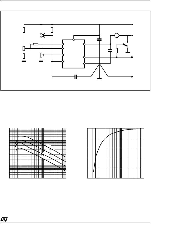
Figure 1: Open Loop Test Circuit.
|
|
|
|
|
|
|
|
|
VREF |
4.7KΩ |
|
|
RT |
|
|
|
|
|
|
|
2N2222 |
|
|
VREF |
|
|
A |
Vi |
|
|
|
|
|
0.1μF |
|
|
|
||
|
100KΩ |
|
COMP |
|
8 |
|
|
|
|
|
|
1 |
|
|
|
|
|||
|
|
|
VFB |
7 |
Vi |
|
|
|
|
ERROR AMP. |
|
|
2 |
|
|
|
1W |
||
ADJUST |
Ω |
|
|
|
0.1 |
μ |
F |
||
|
|
|
|
||||||
|
1K |
|
ISENSE |
|
UC3842A |
|
1KΩ |
||
4.7KΩ |
ISENSE |
|
3 |
OUTPUT |
|
|
|||
|
ADJUST |
Ω |
|
|
6 |
|
|
|
OUTPUT |
|
|
5K |
RT/CT |
|
|
|
|
||
|
|
|
4 |
|
GROUND |
|
|
|
|
|
|
|
|
5 |
|
|
|
||
|
|
|
|
|
|
|
|
|
|
|
|
|
|
|
CT |
|
|
|
|
|
D95IN343 |
|
|
|
|
|
|
|
GROUND |
High peak currentsassociatedwith capacitive loads necessitate careful grounding techniques. Timing and bypass capacitors should be connected close
Figure 2: Oscillator Frequency vs Timing Resistance
fo |
|
|
|
|
D96IN362 |
(Hz) |
|
|
|
|
|
|
|
|
|
|
|
1M |
|
|
|
|
|
|
|
|
|
CT=470pF |
|
|
|
|
|
1nF |
|
100K |
|
|
2. |
|
|
|
|
|
2nF |
|
|
|
|
|
4. |
|
|
|
|
|
7nF |
|
|
10K |
|
|
|
|
|
1K |
|
|
|
|
RT(Ω) |
300 |
1K |
3K |
10K |
30K |
|
to pin 5 in a single point ground. The transistor and 5 KΩ potentiometerareusedto samplethe oscillator waveform and apply an adjustable ramp to pin 3.
Figure 3: Maximum Duty Cycle vs Timing Resistor
fo |
D96IN363 |
|
(Hz) |
||
|
80
60
40
20
0
300 |
1K |
3K |
10K |
30K |
RT(Ω) |
5/15
 Loading...