


 Loading...
ST STM8S105K4, STM8S105K6, STM8S105S4, STM8S105S6, STM8S105C4 User Manual
...STM8S105xx
Access line, 16 MHz STM8S 8-bit MCU, up to 32 Kbytes Flash, integrated EEPROM,10-bit ADC, timers, UART, SPI, I²C
LQFP48 7x7 |
LQFP44 10x10 |
LQFP32 7x7 |
UFQFPN32 5x5 |
SDIP32 400 ml |
Features
Core
•16 MHz advanced STM8 core with Harvard architecture and 3-stage pipeline
•Extended instruction set
Memories
•Medium-density Flash/EEPROM:
-Program memory up to 32 Kbytes; data retention 20 years at 55°C after 10 kcycles
-Data memory up to 1 Kbytes true data EEPROM; endurance 300 kcycles
•RAM: Up to 2 Kbytes
Clock, reset and supply management
•2.95 V to 5.5 V operating voltage
•Flexible clock control, 4 master clock sources:
-Low power crystal resonator oscillator
-External clock input
-Internal, user-trimmable 16 MHz RC
-Internal low power 128 kHz RC
•Clock security system with clock monitor
•Power management:
-Low power modes (wait, active-halt, halt)
-Switch-off peripheral clocks individually
•Permanentlyactive,lowconsumptionpower-on and power-down reset
Interrupt management
•Nested interrupt controller with 32 interrupts
•Up to 37 external interrupts on 6 vectors
Timers
•2x 16-bit general purpose timers, with 2+3 CAPCOM channels (IC, OC or PWM)
•Advanced control timer: 16-bit, 4 CAPCOM channels, 3 complementary outputs, dead-time insertion and flexible synchronization
•8-bit basic timer with 8-bit prescaler
•Auto wake-up timer
•Window and independent watchdog timers
Communications interfaces
•UART with clock output for synchronous operation, Smartcard, IrDA, LIN
•SPI interface up to 8 Mbit/s
•I2C interface up to 400 Kbit/s
Analog-to-digital converter (ADC)
•10-bit, ±1 LSB ADC with up to 10 multiplexed channels, scan mode and analog watchdog
I/Os
•Up to 38 I/Os on a 48-pin package including 16 high sink outputs
•HighlyrobustI/Odesign,immuneagainstcurrent injection
Development support
•Embeddedsinglewireinterfacemodule(SWIM) for fast on-chip programming and non intrusive debugging
Unique ID
• 96-bit unique key for each device
|
Table 1: Device summary |
Reference |
Part number |
STM8S105xx |
STM8S105K4, STM8S105K6, STM8S105S4, |
|
STM8S105S6, STM8S105C4, STM8S105C6 |
June 2012 |
DocID14771 Rev 12 |
1/124 |
www.st.com

Contents |
STM8S105xx |
Contents
1 |
Introduction .............................................................................................................. |
8 |
|
2 |
Description ............................................................................................................... |
9 |
|
3 |
Block diagram ........................................................................................................ |
10 |
|
4 |
Product overview ................................................................................................... |
11 |
|
|
4.1 |
Central processing unit STM8 ..................................................................................... |
11 |
|
4.2 |
Single wire interface module (SWIM) and debug module (DM) .................................. |
11 |
|
4.3 |
Interrupt controller ....................................................................................................... |
12 |
|
4.4 |
Flash program and data EEPROM memory ................................................................ |
12 |
|
4.5 |
Clock controller ............................................................................................................ |
13 |
|
4.6 |
Power management .................................................................................................... |
14 |
|
4.7 Watchdog timers .......................................................................................................... |
15 |
|
|
4.8 |
Auto wakeup counter ................................................................................................... |
15 |
|
4.9 |
Beeper ........................................................................................................................ |
15 |
|
4.10 TIM1 - 16-bit advanced control timer ......................................................................... |
16 |
|
|
4.11 TIM2, TIM3 - 16-bit general purpose timers .............................................................. |
16 |
|
|
4.12 TIM4 - 8-bit basic timer .............................................................................................. |
16 |
|
|
4.13 Analog-to-digital converter (ADC1) ............................................................................ |
17 |
|
|
4.14 Communication interfaces ......................................................................................... |
17 |
|
|
|
4.14.1 UART2 ............................................................................................... |
17 |
|
|
4.14.2 SPI ..................................................................................................... |
18 |
|
|
4.14.3 I²C ...................................................................................................... |
19 |
5 |
Pinout and pin description ................................................................................... |
20 |
|
|
5.1 |
STM8S105 pinouts and pin description ....................................................................... |
21 |
|
|
5.1.1 Alternate function remapping ............................................................... |
27 |
6 Memory and register map ..................................................................................... |
29 |
||
|
6.1 |
Memory map ................................................................................................................ |
29 |
|
6.2 Register map ............................................................................................................... |
30 |
|
|
|
6.2.1 I/O port hardware register map ............................................................ |
30 |
|
|
6.2.2 General hardware register map ........................................................... |
33 |
|
|
6.2.3 CPU/SWIM/debug module/interrupt controller registers ...................... |
44 |
7 |
Interrupt vector mapping ...................................................................................... |
47 |
|
8 |
Option bytes ........................................................................................................... |
49 |
|
9 |
Unique ID |
................................................................................................................ |
54 |
10 Electrical characteristics .................................................................................... |
55 |
||
|
10.1 Parameter conditions ................................................................................................. |
55 |
|
|
|
10.1.1 Minimum and maximum values ......................................................... |
55 |
|
|
10.1.2 Typical values ..................................................................................... |
55 |
2/124 |
DocID14771 Rev 12 |

STM8S105xx |
Contents |
10.1.3 Typical curves .................................................................................... |
55 |
10.1.4 Typical current consumption .............................................................. |
55 |
10.1.5 Loading capacitor ............................................................................... |
56 |
10.1.6 Pin input voltage ................................................................................. |
56 |
10.2 Absolute maximum ratings ........................................................................................ |
56 |
10.3 Operating conditions .................................................................................................. |
58 |
10.3.1 VCAP external capacitor .................................................................... |
61 |
10.3.2 Supply current characteristics ............................................................ |
61 |
10.3.3 External clock sources and timing characteristics ............................. |
73 |
10.3.4 Internal clock sources and timing characteristics ............................... |
75 |
10.3.5 Memory characteristics ...................................................................... |
78 |
10.3.6 I/O port pin characteristics ................................................................. |
79 |
10.3.7 Typical output level curves ................................................................. |
83 |
10.3.8 Reset pin characteristics .................................................................... |
88 |
10.3.9 SPI serial peripheral interface ............................................................ |
91 |
10.3.10 I2C interface characteristics ............................................................. |
94 |
10.3.11 10-bit ADC characteristics ................................................................ |
96 |
10.3.12 EMC characteristics ......................................................................... |
99 |
11 Package information .......................................................................................... |
103 |
11.1 48-pin LQFP package mechanical data ................................................................... |
103 |
11.2 44-pin LQFP package mechanical data ................................................................... |
105 |
11.3 32-pin LQFP package mechanical data ................................................................... |
106 |
11.4 32-lead UFQFPN package mechanical data ........................................................... |
108 |
11.5 SDIP32 package mechanical data ........................................................................... |
109 |
12 Thermal characteristics .................................................................................... |
111 |
12.1 Reference document ............................................................................................... |
112 |
12.2 Selecting the product temperature range ................................................................ |
112 |
13 Ordering information ......................................................................................... |
113 |
13.1 STM8S105 FASTROM microcontroller option list ................................................... |
113 |
14 STM8 development tools .................................................................................. |
118 |
14.1 Emulation and in-circuit debugging tools ................................................................. |
118 |
14.2 Software tools .......................................................................................................... |
118 |
14.2.1 STM8 toolset .................................................................................... |
119 |
14.2.2 C and assembly toolchains .............................................................. |
119 |
14.3 Programming tools .................................................................................................. |
119 |
15 Revision history ................................................................................................. |
120 |
DocID14771 Rev 12 |
3/124 |

List of tables |
STM8S105xx |
List of tables |
|
Table 1. Device summary ......................................................................................................................... |
1 |
Table 2. STM8S105xx access line features ............................................................................................. |
9 |
Table 3. Peripheral clock gating bit assignments in CLK_PCKENR1/2 registers .................................. |
14 |
Table 4. TIM timer features ................................................................................................................... |
16 |
Table 5. Legend/abbreviations for pinout tables ................................................................................... |
20 |
Table 6. Pin description for STM8S105 microcontrollers ....................................................................... |
24 |
Table 7. Flash, Data EEPROM and RAM boundary addresses .......................................................... |
105 |
Table 8. I/O port hardware register map .............................................................................................. |
108 |
Table 9. General hardware register map ................................................................................................ |
33 |
Table 10. CPU/SWIM/debug module/interrupt controller registers ...................................................... |
109 |
Table 11. Interrupt mapping .................................................................................................................... |
47 |
Table 12. Option bytes .......................................................................................................................... |
54 |
Table 13. Option byte description ........................................................................................................... |
50 |
Table 14. Description of alternate function remapping bits [7:0] of OPT2 .............................................. |
52 |
Table 15. Unique ID registers (96 bits) ................................................................................................... |
54 |
Table 16. Voltage characteristics ........................................................................................................... |
56 |
Table 17. Current characteristics ........................................................................................................... |
57 |
Table 18. Thermal characteristics .......................................................................................................... |
58 |
Table 19. General operating conditions ................................................................................................. |
59 |
Table 20. Operating conditions at power-up/power-down ...................................................................... |
60 |
Table 21. Total current consumption with code execution in run mode at VDD = 5 V ............................. |
61 |
Table 22. Total current consumption with code execution in run mode at VDD = 3.3 V .......................... |
73 |
Table 23. Total current consumption in wait mode at VDD = 5 V ............................................................ |
64 |
Table 24. Total current consumption in wait mode at VDD = 3.3 V ......................................................... |
65 |
Table 25. Total current consumption in active halt mode at VDD = 5 V .................................................. |
65 |
Table 26. Total current consumption in active halt mode at VDD = 3.3 V ............................................... |
66 |
Table 27. Total current consumption in halt mode at VDD = 5 V ............................................................. |
67 |
Table 28. Total current consumption in halt mode at VDD = 3.3 V .......................................................... |
68 |
Table 29. Wakeup times ......................................................................................................................... |
68 |
Table 30. Total current consumption and timing in forced reset state .................................................. |
102 |
Table 31. Peripheral current consumption ............................................................................................. |
69 |
Table 32. HSE user external clock characteristics ................................................................................. |
73 |
Table 33. HSE oscillator characteristics ................................................................................................. |
74 |
Table 34. HSI oscillator characteristics .................................................................................................. |
75 |
Table 35. LSI oscillator characteristics ................................................................................................... |
77 |
Table 36. RAM and hardware registers .................................................................................................. |
78 |
Table 37. Flash program memory/data EEPROM memory .................................................................... |
78 |
Table 38. I/O static characteristics ......................................................................................................... |
79 |
Table 39. Output driving current (standard ports) .................................................................................. |
82 |
Table 40. Output driving current (true open drain ports) ........................................................................ |
82 |
Table 41. Output driving current (high sink ports) .................................................................................. |
83 |
Table 42. NRST pin characteristics ........................................................................................................ |
88 |
Table 43. SPI characteristics .................................................................................................................. |
91 |
Table 44. I2C characteristics .................................................................................................................. |
94 |
Table 45. ADC characteristics ................................................................................................................ |
96 |
Table 46. ADC accuracy with RAIN < 10 kΩ , VDDA= 5 V ....................................................................... |
97 |
Table 47. ADC accuracy with RAIN < 10 kΩ RAIN, VDDA = 3.3 V ............................................................ |
98 |
4/124 |
DocID14771 Rev 12 |

STM8S105xx |
List of tables |
Table 48. EMS data .............................................................................................................................. |
100 |
|
Table 49. EMI data ............................................................................................................................... |
101 |
|
Table 50. ESD absolute maximum ratings ........................................................................................... |
102 |
|
Table 51. Electrical sensitivities ........................................................................................................... |
102 |
|
Table 52. 48-pin low profile quad flat package mechanical data ......................................................... |
103 |
|
Table 53. 44-pin low profile quad flat package mechanical data ......................................................... |
105 |
|
Table 54. 32-pin low profile quad flat package mechanical data ......................................................... |
120 |
|
Table 55. 32-lead, ultra thin, fine pitch quad flat no-lead package mechanical data ........................... |
108 |
|
Table 56. |
32-lead shrink plastic DIP (400 ml) package mechanical data ............................................ |
109 |
Table 57. |
Thermal characteristics(1) .................................................................................................... |
111 |
Table 58. |
Document revision history ................................................................................................... |
120 |
DocID14771 Rev 12 |
5/124 |

List of figures |
STM8S105xx |
List of figures |
|
Figure 1. STM8S105xx access line block diagram ................................................................................ |
10 |
Figure 2. Flash memory organisation .................................................................................................... |
13 |
Figure 3. LQFP 48-pin pinout ................................................................................................................. |
21 |
Figure 4. LQFP 44-pin pinout ................................................................................................................. |
22 |
Figure 5. LQFP/UFQFPN 32-pin pinout ................................................................................................ |
23 |
Figure 6. SDIP 32-pin pinout .................................................................................................................. |
24 |
Figure 7. Memory map ........................................................................................................................... |
29 |
Figure 8. Supply current measurement conditions ................................................................................ |
55 |
Figure 9. Pin loading conditions ............................................................................................................. |
56 |
Figure 10. Pin input voltage ................................................................................................................... |
56 |
Figure 11. fCPUmax versus VDD .............................................................................................................. |
60 |
Figure 12. External capacitor CEXT ....................................................................................................... |
61 |
Figure 13. Typ. IDD(RUN) vs. VDD , HSE user external clock, fCPU = 16 MHz ........................................... |
70 |
Figure 14. Typ. IDD(RUN) vs. fCPU , HSE user external clock, VDD= 5 V .................................................. |
71 |
Figure 15. Typ. IDD(RUN) vs. VDD , HSI RC osc, fCPU = 16 MHz .............................................................. |
71 |
Figure 16. Typ. IDD(WFI) vs. VDD , HSE user external clock, fCPU = 16 MHz ............................................ |
72 |
Figure 17. Typ. IDD(WFI) vs. fCPU, HSE user external clock VDD = 5 V .................................................... |
72 |
Figure 18. Typ. IDD(WFI) vs. VDD, HSI RC osc, fCPU = 16 MHz ................................................................ |
73 |
Figure 19. HSE external clocksource ..................................................................................................... |
74 |
Figure 20. HSE oscillator circuit diagram ............................................................................................... |
75 |
Figure 21. Typical HSI accuracy at VDD = 5 V vs 5 temperatures .......................................................... |
76 |
Figure 22. Typical HSI accuracy vs VDD @ 4 temperatures .................................................................. |
77 |
Figure 23. Typical LSI accuracy vs VDD @ 4 temperatures ................................................................... |
78 |
Figure 24. Typical VIL and VIH vs VDD @ 4 temperatures ...................................................................... |
81 |
Figure 25. Typical pull-up resistance vs VDD @ 4 temperatures ............................................................ |
81 |
Figure 26. Typical pull-up current vs VDD @ 4 temperatures ................................................................. |
82 |
Figure 27. Typ. VOL @ VDD = 5 V (standard ports) ................................................................................ |
84 |
Figure 28. Typ. VOL @ VDD = 3.3 V (standard ports) ............................................................................. |
84 |
Figure 29. Typ. VOL @ VDD = 5 V (true open drain ports) ...................................................................... |
85 |
Figure 30. Typ. VOL @ VDD = 3.3 V (true open drain ports) ................................................................... |
85 |
Figure 31. Typ. VOL @ VDD = 5 V (high sink ports) ................................................................................ |
86 |
Figure 32. Typ. VOL @ VDD = 3.3 V (high sink ports) ............................................................................. |
86 |
Figure 33. Typ. VDD - VOH @ VDD = 5 V (standard ports) ....................................................................... |
87 |
Figure 34. Typ. VDD - VOH @ VDD = 3.3 V (standard ports) .................................................................... |
87 |
Figure 35. Typ. VDD - VOH @ VDD = 5 V (high sink ports) ...................................................................... |
88 |
Figure 36. Typ. VDD - VOH @ VDD = 3.3 V (high sink ports) ................................................................... |
88 |
Figure 37. Typical NRST VIL and VIH vs VDD @ 4 temperatures ........................................................... |
89 |
Figure 38. Typical NRST pull-up resistance vs VDD @ 4 temperatures ................................................. |
90 |
Figure 39. Typical NRST pull-up current vs VDD @ 4 temperatures ...................................................... |
90 |
Figure 40. Recommended reset pin protection ...................................................................................... |
91 |
Figure 41. SPI timing diagram - slave mode and CPHA = 0 .................................................................. |
93 |
Figure 42. SPI timing diagram - slave mode and CPHA = 1(1) ............................................................. |
93 |
Figure 43. SPI timing diagram - master mode(1) ................................................................................... |
94 |
Figure 44. Typical application with I2C bus and timing diagram (1) ....................................................... |
95 |
Figure 45. ADC accuracy characteristics ............................................................................................... |
99 |
Figure 46. Typical application with ADC ................................................................................................ |
99 |
Figure 47. 48-pin low profile quad flat package (7 x 7) ........................................................................ |
103 |
6/124 |
DocID14771 Rev 12 |

STM8S105xx |
List of figures |
Figure 48. 44-pin low profile quad flat package ................................................................................... |
105 |
|
Figure 49. 32-pin low profile quad flat package (7 x 7) ........................................................................ |
106 |
|
Figure 50. |
32-lead, ultra thin, fine pitch quad flat no-lead package (5 x 5) .......................................... |
108 |
Figure 51. 32-lead shrink plastic DIP (400 ml) package ...................................................................... |
109 |
|
Figure 52. |
STM8S105xx access line ordering information scheme ..................................................... |
113 |
DocID14771 Rev 12 |
7/124 |

Introduction |
STM8S105xx |
1Introduction
Thisdatasheetcontainsthedescriptionofthedevicefeatures,pinout,electricalcharacteristics, mechanical data and ordering information.
•ForcompleteinformationontheSTM8Smicrocontrollermemory,registersandperipherals, please refer to the STM8S microcontroller family reference manual (RM0016).
•For information on programming, erasing and protection of the internal Flash memory please refer to the STM8S Flash programming manual (PM0051).
•For information on the debug and SWIM (single wire interface module) refer to the STM8 SWIM communication protocol and debug module user manual (UM0470).
•For information on the STM8 core, please refer to the STM8 CPU programming manual (PM0044).
8/124 |
DocID14771 Rev 12 |

STM8S105xx |
Description |
2Description
TheSTM8S105xxaccessline8-bitmicrocontrollersofferfrom16to32KbytesFlashprogram memory,plusintegratedtruedataEEPROM. Theyarereferredtoasmedium-densitydevices in the STM8S microcontroller family reference manual (RM0016).
All devices of the STM8S105xx access line provide the following benefits: reduced system cost, performance and robustness, short development cycles, and product longevity.
The system cost is reduced thanks to an integrated true data EEPROM for up to 300 kwrite/erasecyclesandahighsystemintegrationlevelwithinternalclockoscillators,watchdog, and brown-out reset.
Device performance is ensured by a 16 MHz CPU clock frequency and enhanced characteristics which include robust I/O, independent watchdogs (with a separate clock source), and a clock security system.
Short development cycles are guaranteed due to application scalability across a common familyproductarchitecturewithcompatiblepinout,memorymapandandmodularperipherals. Full documentation is offered with a wide choice of development tools.
Product longevity is ensured in the STM8S family thanks to their advanced core which is made in a state-of-the art technology for applications with 2.95 V to 5.5 V operating supply.
Table 2: STM8S105xx access line features
Device |
STM8S105C6 |
STM8S105C4 |
STM8S105S6 |
STM8S105S4 |
STM8S105K6 |
STM8S105K4 |
Pin count |
48 |
48 |
44 |
44 |
32 |
32 |
Maximumnumber |
38 |
38 |
34 |
34 |
25 |
25 |
of GPIOs |
|
|
|
|
|
|
Ext. Interrupt pins |
35 |
35 |
31 |
31 |
23 |
23 |
Timer CAPCOM |
9 |
9 |
8 |
8 |
8 |
8 |
channels |
|
|
|
|
|
|
Timer |
3 |
3 |
3 |
3 |
3 |
3 |
complementary |
|
|
|
|
|
|
outputs |
|
|
|
|
|
|
A/D Converter |
10 |
10 |
9 |
9 |
7 |
7 |
channels |
|
|
|
|
|
|
High sink I/Os |
16 |
16 |
15 |
15 |
12 |
12 |
Medium density |
32K |
16K |
32K |
16K |
32K |
16K |
Flash Program |
|
|
|
|
|
|
memory (bytes) |
|
|
|
|
|
|
Data EEPROM |
1024 |
1024 |
1024 |
1024 |
1024 |
1024 |
(bytes) |
|
|
|
|
|
|
RAM (bytes) |
2K |
2K |
2K |
2K |
2K |
2K |
Peripheral set |
Advancedcontroltimer(TIM1),General-purposetimers(TIM2andTIM3),Basictimer(TIM4)SPI,I2C,UART, |
|||||
|
Window WDG, Independent WDG, ADC |
|
|
|
||
DocID14771 Rev 12 |
9/124 |
Block diagram |
STM8S105xx |
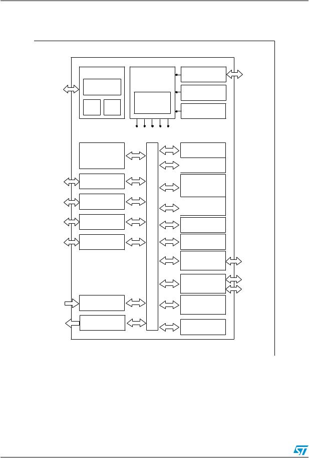
3Block diagram
Figure 1: STM8S105xx access line block diagram
|
Reset block |
|
XTAL 1-16 MHz |
|
|
|
|
|
Clock controller |
|
|
Reset |
|
Reset |
|
RC int. 16 MHz |
|
|
|
|
|
|
|
|
POR |
BOR |
Detector |
|
|
|
|
RC int. 128 kHz |
|
||
|
|
|
|
|
|
|
|
|
Clock to peripherals and core |
|
|
|
|
|
|
Window WDG |
|
|
STM8 core |
|
|
|
|
|
|
|
|
Independent WDG |
|
Single wire |
Debug/SWIM |
|
Up to 32 Kbytes |
|
|
debug interf. |
|
|
|||
|
|
|
program Flash |
|
|
|
|
|
|
|
|
Master/slave |
|
|
|
|
|
autosynchro |
UART2 |
|
1 Kbytes |
|
|
LIN master |
|
|
|||
|
|
|
|
||
|
|
|
data EEPROM |
|
|
SPI emul. |
|
|
|
|
|
|
|
bus |
|
|
|
|
|
I2C |
|
|
|
400 Kbit/s |
|
data |
Up to 2 Kbytes |
|
|
|
|
|
RAM |
|
|
|
|
|
and |
|
|
|
|
|
|
|
|
8 Mbit/s |
|
SPI |
Address |
Boot ROM |
|
|
|
|
|
Up to |
|
|
|
|
|
|
|
|
|
|
|
16-bit advanced control |
4 CAPCOM |
|
|
|
|
channels +3 |
|
|
|
|
|
timer (TIM1) |
|
|
|
|
|
complementary |
|
|
|
|
|
|
|
|
|
|
|
|
outputs |
|
|
|
|
16-bit general purpose |
Up to |
|
|
|
|
5 CAPCOM |
|
|
|
|
|
timers (TIM2, TIM3) |
|
|
|
|
|
channels |
|
|
|
|
|
|
|
Up to 10 channels |
|
ADC1 |
|
8-bit basic timer |
|
|
|
|
|
||
|
|
|
|
(TIM4) |
|
1/2/4 kHz |
Beeper |
|
|
|
|
beep |
|
AWU timer |
|
||
|
|
|
|
||
|
|
|
|
|
|
10/124 |
DocID14771 Rev 12 |
STM8S105xx |
Product overview |
4Product overview
Thefollowingsectionintendstogiveanoverviewofthebasicfeaturesofthedevicefunctional modules and peripherals.
For more detailed information please refer to the corresponding family reference manual (RM0016).
4.1Central processing unit STM8
The 8-bit STM8 core is designed for code efficiency and performance.
It contains 6 internal registers which are directly addressable in each execution context, 20 addressing modes including indexed indirect and relative addressing and 80 instructions.
Architecture and registers
•Harvard architecture
•3-stage pipeline
•32-bit wide program memory bus - single cycle fetching for most instructions
•X and Y 16-bit index registers - enabling indexed addressing modes with or without offset and read-modify-write type data manipulations
•8-bit accumulator
•24-bit program counter - 16-Mbyte linear memory space
•16-bit stack pointer - access to a 64 K-level stack
•8-bit condition code register - 7 condition flags for the result of the last instruction
Addressing
•20 addressing modes
•Indexed indirect addressing mode for look-up tables located anywhere in the address space
•Stack pointer relative addressing mode for local variables and parameter passing
Instruction set
•80 instructions with 2-byte average instruction size
•Standard data movement and logic/arithmetic functions
•8-bit by 8-bit multiplication
•16-bit by 8-bit and 16-bit by 16-bit division
•Bit manipulation
•Data transfer between stack and accumulator (push/pop) with direct stack access
•Data transfer using the X and Y registers or direct memory-to-memory transfers
4.2Single wire interface module (SWIM) and debug module (DM)
Thesinglewireinterfacemoduleanddebugmodulepermitsnon-intrusive,real-timein-circuit debugging and fast memory programming.
DocID14771 Rev 12 |
11/124 |

Product overview |
STM8S105xx |
SWIM
Singlewireinterfacemodulefordirectaccesstothedebugmoduleandmemoryprogramming. Theinterfacecanbeactivatedinalldeviceoperationmodes. Themaximumdatatransmission speed is 145 bytes/ms.
Debug module
Thenon-intrusivedebuggingmodulefeaturesaperformanceclosetoafull-featuredemulator. Besidememoryandperipherals,alsoCPUoperationcanbemonitoredinreal-timebymeans of shadow registers.
•R/W to RAM and peripheral registers in real-time
•R/W access to all resources by stalling the CPU
•Breakpoints on all program-memory instructions (software breakpoints)
•Two advanced breakpoints, 23 predefined configurations
4.3Interrupt controller
•Nested interrupts with three software priority levels
•32 interrupt vectors with hardware priority
•Up to 37 external interrupts on 6 vectors including TLI
•Trap and reset interrupts
4.4Flash program and data EEPROM memory
•Up to 32 Kbytes of Flash program single voltage Flash memory
•Up to 1 Kbytes true data EEPROM
•Readwhilewrite:Writingindatamemorypossiblewhileexecutingcodeinprogrammemory
•User option byte area
Write protection (WP)
WriteprotectionofFlashprogrammemoryanddataEEPROMisprovidedtoavoidunintentional overwriting of memory that could result from a user software malfunction.
There are two levels of write protection. The first level is known as MASS (memory access security system). MASS is always enabled and protects the main Flash program memory, data EEPROM and option bytes.
To perform in-application programming (IAP), this write protection can be removed by writing a MASS key sequence in a control register. This allows the application to write to data EEPROM, modify the contents of main program memory or the device option bytes.
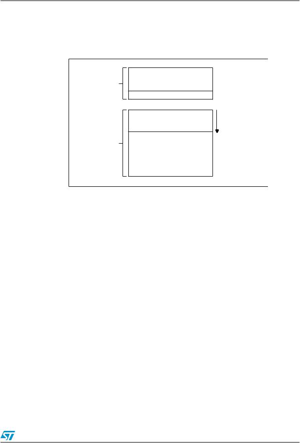
Asecondlevelofwriteprotection,canbeenabledtofurtherprotectaspecificareaofmemory known as UBC (user boot code). Refer to the figure below.
The size of the UBC is programmable through the UBC option byte, in increments of 1 page (512 bytes) by programming the UBC option byte in ICP mode.
This divides the program memory into two areas:
•Main program memory: Up to 32 Kbytes minus UBC
•User-specific boot code (UBC): Configurable up to 32 Kbytes
12/124 |
DocID14771 Rev 12 |
STM8S105xx |
Product overview |
The UBC area remains write-protected during in-application programming. This means that the MASS keys do not unlock the UBC area. It protects the memory used to store the boot program, specific code libraries, reset and interrupt vectors, the reset routine and usually the IAP and communication routines.
Figure 2: Flash memory organisation
Data EEPROM memory
Medium density
Flash program memory (up to 32 Kbytes)
Data memory area ( 1 Kbyte)
Option bytes
UBC area
Remains write protected during IAP
Program memory area
Write access possible for IAP
Programmable area from 1 Kbyte
(2 first pages) up to
32 Kbytes
(1 page steps)
Read-out protection (ROP)
The read-out protection blocks reading and writing the Flash program memory and data EEPROMmemoryinICPmode(anddebugmode). Oncetheread-outprotectionisactivated, anyattempttotoggleitsstatustriggersaglobaleraseoftheprogramanddatamemory. Even if no protection can be considered as totally unbreakable, the feature provides a very high level of protection for a general purpose microcontroller.
4.5Clock controller
The clock controller distributes the system clock (fMASTER) coming from different oscillators tothecoreandtheperipherals. Italsomanagesclockgatingforlowpowermodesandensures
clock robustness.
Features
•Clock prescaler: To get the best compromise between speed and current consumption the clock frequency to the CPU and peripherals can be adjusted by a programmable prescaler.
•Safe clock switching: Clock sources can be changed safely on the fly in run mode throughaconfigurationregister. Theclocksignalisnotswitcheduntilthenewclocksource is ready. The design guarantees glitch-free switching.
•Clock management: To reduce power consumption, the clock controller can stop the clock to the core, individual peripherals or memory.
•Master clock sources: Four different clock sources can be used to drive the master clock:
-1-16 MHz high-speed external crystal (HSE)
-Up to 16 MHz high-speed user-external clock (HSE user-ext)
DocID14771 Rev 12 |
13/124 |

Product overview |
STM8S105xx |
-16 MHz high-speed internal RC oscillator (HSI)
-128 kHz low-speed internal RC (LSI)
•Startup clock: After reset, the microcontroller restarts by default with an internal 2 MHz clock (HSI/8). The prescaler ratio and clock source can be changed by the application program as soon as the code execution starts.
•Clock security system (CSS): This feature can be enabled by software. If an HSE clock failure occurs, the internal RC (16 MHz/8) is automatically selected by the CSS and an interrupt can optionally be generated.
•Configurable main clock output (CCO): This outputs an external clock for use by the application.
Table 3: Peripheral clock gating bit assignments in CLK_PCKENR1/2 registers
Bit |
Peripheral |
Bit |
Peripheral |
Bit |
Peripheral |
Bit |
Peripheral |
|
clock |
|
clock |
|
clock |
|
clock |
PCKEN1 7 |
TIM1 |
PCKEN1 3 |
UART2 |
PCKEN2 7 |
Reserved |
PCKEN2 3 |
ADC |
PCKEN1 6 |
TIM3 |
PCKEN1 2 |
Reserved |
PCKEN2 6 |
Reserved |
PCKEN2 2 |
AWU |
PCKEN1 5 |
TIM2 |
PCKEN1 1 |
SPI |
PCKEN2 5 |
Reserved |
PCKEN2 1 |
Reserved |
PCKEN1 4 |
TIM4 |
PCKEN1 0 |
I2C |
PCKEN2 4 |
Reserved |
PCKEN2 0 |
Reserved |
4.6Power management
For efficent power management, the application can be put in one of four different low-power modes. You can configure each mode to obtain the best compromise between lowest power consumption, fastest start-up time and available wakeup sources.
•Wait mode: In this mode, the CPU is stopped, but peripherals are kept running. The wakeup is performed by an internal or external interrupt or reset.
•Active halt mode with regulator on: In this mode, the CPU and peripheral clocks are stopped. An internal wakeup is generated at programmable intervals by the auto wake up unit (AWU). The main voltage regulator is kept powered on, so current consumption is higher than in active halt mode with regulator off, but the wakeup time is faster. Wakeup is triggered by the internal AWU interrupt, external interrupt or reset.
•Active halt mode with regulator off: This mode is the same as active halt with regulator on, except that the main voltage regulator is powered off, so the wake up time is slower.
•Halt mode: Inthismodethemicrocontrollerusestheleastpower. TheCPUandperipheral clocks are stopped, the main voltage regulator is powered off. Wakeup is triggered by external event or reset.
14/124 |
DocID14771 Rev 12 |

STM8S105xx |
Product overview |
4.7Watchdog timers
The watchdog system is based on two independent timers providing maximum security to the applications.
Activationofthewatchdogtimersiscontrolledbyoptionbytesorbysoftware. Onceactivated, the watchdogs cannot be disabled by the user program without performing a reset.
Window watchdog timer
The window watchdog is used to detect the occurrence of a software fault, usually generated by external interferences or by unexpected logical conditions, which cause the application program to abandon its normal sequence.
The window function can be used to trim the watchdog behavior to match the application perfectly.
The application software must refresh the counter before time-out and during a limited time window.
A reset is generated in two situations:
1.Timeout: At 16 MHz CPU clock the time-out period can be adjusted between 75 µs up to 64 ms.
2.Refresh out of window: The downcounter is refreshed before its value is lower than the one stored in the window register.
Independent watchdog timer
The independent watchdog peripheral can be used to resolve processor malfunctions due to hardware or software failures.
It is clocked by the 128 kHZ LSI internal RC clock source, and thus stays active even in case of a CPU clock failure
The IWDG time base spans from 60 µs to 1 s.
4.8Auto wakeup counter
•Used for auto wakeup from active halt mode
•Clock source: Internal 128 kHz internal low frequency RC oscillator or external clock
•LSI clock can be internally connected to TIM3 input capture channel 1 for calibration
4.9Beeper
The beeper function outputs a signal on the BEEP pin for sound generation. The signal is in the range of 1, 2 or 4 kHz.
ThebeeperoutputportisonlyavailablethroughthealternatefunctionremapoptionbitAFR7.
DocID14771 Rev 12 |
15/124 |

Product overview |
STM8S105xx |
4.10TIM1 - 16-bit advanced control timer
This is a high-end timer designed for a wide range of control applications. With its complementary outputs, dead-time control and center-aligned PWM capability, the field of applications is extended to motor control, lighting and half-bridge driver
•16-bit up, down and up/down autoreload counter with 16-bit prescaler
•Four independent capture/compare channels (CAPCOM) configurable as input capture, outputcompare,PWMgeneration(edgeandcenteralignedmode)andsinglepulsemode output
•Synchronization module to control the timer with external signals
•Break input to force the timer outputs into a defined state
•Three complementary outputs with adjustable dead time
•Encoder mode
•Interrupt sources: 3 x input capture/output compare, 1 x overflow/update, 1 x break
4.11TIM2, TIM3 - 16-bit general purpose timers
•16-bit autoreload (AR) up-counter
•15-bit prescaler adjustable to fixed power of 2 ratios 1…32768
•Timers with 3 or 2 individually configurable capture/compare channels
•PWM mode
•Interrupt sources: 2 or 3 x input capture/output compare, 1 x overflow/update
4.12TIM4 - 8-bit basic timer
•8-bit autoreload, adjustable prescaler ratio to any power of 2 from 1 to 128
•Clock source: CPU clock
•Interrupt source: 1 x overflow/update
|
|
Table 4: TIM timer features |
|
|
|||
Timer |
Counter Prescaler |
Counting CAPCOM |
Complem. Ext. |
Timer |
|||
|
size |
|
mode |
channels |
outputs |
trigger synchronization/ |
|
|
(bits) |
|
|
|
|
|
chaining |
TIM1 |
16 |
Any integer from 1 to |
Up/ |
4 |
3 |
Yes |
No |
|
|
65536 |
down |
|
|
|
|
TIM2 |
16 |
Any power of 2 from |
Up |
3 |
0 |
No |
|
|
|
1 to 32768 |
|
|
|
|
|
TIM3 |
16 |
Any power of 2 from |
Up |
2 |
0 |
No |
|
|
|
1 to 32768 |
|
|
|
|
|
16/124 |
DocID14771 Rev 12 |

STM8S105xx |
|
|
|
|
Product overview |
|
Timer |
Counter Prescaler |
Counting CAPCOM |
Complem. Ext. Timer |
|||
|
size |
|
mode |
channels |
outputs |
trigger synchronization/ |
|
(bits) |
|
|
|
|
chaining |
TIM4 |
8 |
Any power of 2 from |
Up |
0 |
0 |
No |
|
|
1 to 128 |
|
|
|
|
4.13Analog-to-digital converter (ADC1)
TheSTM8S105xxproductscontaina10-bitsuccessiveapproximationA/Dconverter(ADC1) with up to 10 multiplexed input channels and the following main features:
•Input voltage range: 0 to VDDA
•Conversion time: 14 clock cycles
•Single and continuous and buffered continuous conversion modes
•Buffer size (n x 10 bits) where n = number of input channels
•Scan mode for single and continuous conversion of a sequence of channels
•Analog watchdog capability with programmable upper and lower thresholds
•Analog watchdog interrupt
•External trigger input
•Trigger from TIM1 TRGO
•End of conversion (EOC) interrupt
Note: Additional AIN12 analog input is not selectable in ADC scan mode or with analog watchdog. Values converted from AIN12 are stored only into the ADC_DRH/ADC_DRL registers.
4.14Communication interfaces
The following communication interfaces are implemented:
•UART2: Full feature UART, synchronous mode, SPI master mode, Smartcard mode, IrDA mode, LIN2.1 master/slave capability
•SPI : Full and half-duplex, 8 Mbit/s
•I²C: Up to 400 Kbit/s
4.14.1UART2
Main features
•One Mbit/s full duplex SCI
•SPI emulation
•High precision baud rate generator
•Smartcard emulation
•IrDA SIR encoder decoder
DocID14771 Rev 12 |
17/124 |

Product overview |
STM8S105xx |
•LIN master mode
•LIN slave mode
Asynchronous communication (UART mode)
•Full duplex communication - NRZ standard format (mark/space)
•Programmable transmit and receive baud rates up to 1 Mbit/s (fCPU/16) and capable of following any standard baud rate regardless of the input frequency
•Separate enable bits for transmitter and receiver
•Two receiver wakeup modes:
-Address bit (MSB)
-Idle line (interrupt)
•Transmission error detection with interrupt generation
•Parity control
Synchronous communication
•Full duplex synchronous transfers
•SPI master operation
•8-bit data communication
•Maximum speed: 1 Mbit/s at 16 MHz (fCPU/16)
LIN master mode
•Emission: Generates 13-bit synch break frame
•Reception: Detects 11-bit break frame
LIN slave mode
•Autonomous header handling - one single interrupt per valid message header
•Automatic baud rate synchronization - maximum tolerated initial clock deviation ±15 %
•Synch delimiter checking
•11-bit LIN synch break detection - break detection always active
•Parity check on the LIN identifier field
•LIN error management
•Hot plugging support
4.14.2SPI
•Maximum speed: 8 Mbit/s (fMASTER/2) both for master and slave
•Full duplex synchronous transfers
•Simplex synchronous transfers on two lines with a possible bidirectional data line
•Master or slave operation - selectable by hardware or software
•CRC calculation
•1 byte Tx and Rx buffer
•Slave/master selection input pin
18/124 |
DocID14771 Rev 12 |

STM8S105xx |
Product overview |
4.14.3I²C
•I²C master features:
-Clock generation
-Start and stop generation
•I²C slave features:
-Programmable I2C address detection
-Stop bit detection
•Generation and detection of 7-bit/10-bit addressing and general call
•Supports different communication speeds:
-Standard speed (up to 100 kHz)
-Fast speed (up to 400 kHz)
DocID14771 Rev 12 |
19/124 |

Pinout and pin description |
STM8S105xx |
5Pinout and pin description
|
Table 5: Legend/abbreviations for pinout tables |
|
Type |
I= Input, O = Output, S = Power supply |
|
Level |
Input |
CM = CMOS |
|
Output |
HS = High sink |
Output speed |
O1 = Slow (up to 2 MHz) |
|
|
||
|
O2 = Fast (up to 10 MHz) |
|
|
O3=Fast/slowprogrammabilitywithslowasdefaultstateafterreset |
|
|
O4 = Fast/slow programmability with fast as default state after reset |
|
Port and control |
Input |
float = floating, wpu = weak pull-up |
configuration |
Output |
T = True open drain, OD = Open drain, PP = |
|
||
Push pull
Reset state
Bold X (pin state after internal reset release).
Unlessotherwisespecified,thepinstateisthesameduringthereset phase and after the internal reset release.
20/124 |
DocID14771 Rev 12 |
STM8S105xx |
Pinout and pin description |
5.1STM8S105 pinouts and pin description
Figure 3: LQFP 48-pin pinout
|
|
|
|
|
|
|
[BEEP] |
[ADC_ETR] |
[TIM2_CH3] |
|
|
[TIM1_BKIN] [CLK_CCO] |
|
|
|
|
|
|||
|
PD7/TLI [TIM1_CH4] |
PD6/UART2_RX |
PD5/UART2_TX |
PD4 (HS)/TIM2_CH1 |
PD3 (HS)/TIM2_CH2 |
PD2 (HS)/TIM3_CH1 |
PD1 (HS)/SWIM |
PD0 (HS)/TIM3_CH2 |
PE0 (HS)/CLK_CCO PE1 (T)/I2C_SCL |
PE2 (T)/I2C_SDAA |
PE3/TIM1_BKIN |
|
||||||||
|
48 47 46 45 |
|
44 43 42 41 40 39 38 37 |
PG1 |
||||||||||||||||
NRST |
1 |
|
|
|
|
|
|
|
|
|
|
|
|
|
|
|
|
|
36 |
|
OSCIN/PA1 |
2 |
|
|
|
|
|
|
|
|
|
|
|
|
|
|
|
|
|
35 |
PG0 |
|
|
|
|
|
|
|
|
|
|
|
|
|
|
|
|
|
PC7 (HS)/SPI_MISO |
|||
OSCOUT/PA2 |
3 |
|
|
|
|
|
|
|
|
|
|
|
|
|
|
|
|
|
34 |
|
|
|
|
|
|
|
|
|
|
|
|
|
|
|
|
|
|
PC6 (HS)/SPI_MOSI |
|||
VSSIO_1 |
4 |
|
|
|
|
|
|
|
|
|
|
|
|
|
|
|
|
|
33 |
|
|
|
|
|
|
|
|
|
|
|
|
|
|
|
|
|
|
|
|||
VSS |
5 |
|
|
|
|
|
|
|
|
|
|
|
|
|
|
|
|
|
32 |
VDDIO_2 |
VCAP |
6 |
|
|
|
|
|
|
|
|
|
|
|
|
|
|
|
|
|
31 |
VSSIO_2 |
VDD |
7 |
|
|
|
|
|
|
|
|
|
|
|
|
|
|
|
|
|
30 |
PC5 (HS)/SPI_SCK |
VDDIO_1 |
8 |
|
|
|
|
|
|
|
|
|
|
|
|
|
|
|
|
|
29 |
PC4 (HS)/TIM1_CH4 |
|
|
|
|
|
|
|
|
|
|
|
|
|
|
|
|
|
|
PC3 (HS)/TIM1_CH3 |
||
[TIM3_CH1] TIM2_CH3/PA3 |
9 |
|
|
|
|
|
|
|
|
|
|
|
|
|
|
|
|
|
28 |
|
|
|
|
|
|
|
|
|
|
|
|
|
|
|
|
|
|
|
PC2 (HS)/TIM1_CH2 |
||
(HS) PA4 |
10 |
|
|
|
|
|
|
|
|
|
|
|
|
|
|
|
|
|
27 |
|
|
|
|
|
|
|
|
|
|
|
|
|
|
|
|
|
|
|
PC1 (HS)/TIM1_CH1/UART2_CK |
||
(HS) PA5 |
11 |
|
|
|
|
|
|
|
|
|
|
|
|
|
|
|
|
|
26 |
|
|
|
|
|
|
|
|
|
|
|
|
|
|
|
|
|
|
|
PE5/SPI_NSS |
||
(HS) PA6 |
12 |
|
|
|
|
|
|
|
|
|
|
|
|
|
|
|
|
|
25 |
|
13 |
14 |
15 |
16 |
17 |
18 |
19 |
20 |
21 |
22 23 24 |
|
||||||||||
|
|
|||||||||||||||||||
|
VDDA |
|
VSSA |
|
AIN7/PB7 |
|
AIN6/PB6 |
|
[I2C_SDA] AIN5/PB5 |
|
[I2C_SCL] AIN4/PB4 |
|
[TIM1_ETR] AIN3/PB3 |
|
[TIM1_CH3N] AIN2/PB2 |
[TIM1_CH2N] AIN1/PB1 |
[TIM1_CH1N] AIN0/PB0 |
AIN8/PE7 |
AIN9/PE6 |
|
1.(HS) high sink capability.
2.(T) True open drain (P-buffer and protection diode to VDD not implemented).
3.[ ] alternate function remapping option (If the same alternate function is shown twice, it indicates an exclusive choice not a duplication of the function).
DocID14771 Rev 12 |
21/124 |

Pinout and pin description |
STM8S105xx |
Figure 4: LQFP 44-pin pinout
|
|
|
[BEEP] |
[ADC_ETR] |
[TIM2_CH3] |
|
[TIM1_BKIN] [CLK_CCO] |
|
|
|
PD7/TLI [TIM1_CH4] |
PD6/UART2_RX |
PD5/UART2_TX |
PD4 (HS)/TIM2_CH1 |
PD3 (HS)/TIM2_CH2 |
PD2 (HS)/TIM3_CH1 |
PD1 (HS)/SWIM |
PD0 (HS)/TIM3_CH2 |
PE0 (HS)/CLK_CCO |
PE1 (T)/I2C_SCL |
PE2 (T)/I2C_SDA |
44 |
43 |
42 |
41 |
40 |
39 |
38 |
37 |
36 |
35 |
34 |
NRST |
1 |
33 |
OSCIN/PA1 |
2 |
32 |
OSCOUT/PA2 |
3 |
31 |
VSSIO_1 |
4 |
30 |
VSS |
5 |
29 |
VCAP |
6 |
28 |
VDD |
7 |
27 |
VDDIO_1 |
8 |
26 |
(HS) PA4 |
9 |
25 |
(HS) PA5 |
10 |
24 |
(HS) PA6 |
11 |
23 |
12 |
13 |
14 |
15 |
16 |
17 |
18 |
19 |
20 |
21 |
22 |
VDDA |
VSSA |
AIN7/PB7 |
AIN6/PB6 |
AIN5/PB5 |
AIN4/PB4 |
AIN3/PB3 |
AIN2/PB2 |
AIN1/PB1 |
AIN0/PB0 |
AIN9/PE6 |
|
|
|
|
[I2C_SDA] |
[I2C_SCL] |
[TIM1_ETR] |
[TIM1_CH3N] |
[TIM1_CH2N] |
[TIM1_CH1N] |
|
PG1
PG0
PC7 (HS)/SPI_MISO PC6 (HS)/SPI_MOSI VDDIO_2
VSSIO_2
PC5 (HS)/SPI_SCK
PC3 (HS)/TIM1_CH3 PC2 (HS)/TIM1_CH2 PC1 (HS)/TIM1_CH1 PE5/SPI_NSS/UART2_CK
1.(HS) high sink capability.
2.(T) True open drain (P-buffer and protection diode to VDD not implemented).
3.[ ] alternate function remapping option (If the same alternate function is shown twice, it indicates an exclusive choice not a duplication of the function).
22/124 |
DocID14771 Rev 12 |

STM8S105xx |
Pinout and pin description |
Figure 5: LQFP/UFQFPN 32-pin pinout
|
|
|
[BEEP] |
[ADC_ETR] |
[TIM2_CH3] |
|
[TIM1_BKIN] [CLK_CCO] |
PD7/TLI [TIM1_CH4] |
PD6/UART2_RX |
PD5/UART2_TX |
PD4 (HS)/TIM2_CH1 |
PD3 (HS)/TIM2_CH2 |
PD2 (HS)/TIM3_CH1 |
PD1 (HS)/SWIM |
PD0 (HS)/TIM3_CH2 |
32 |
31 |
30 |
29 |
28 |
27 |
26 |
25 |
NRST |
1 |
|
|
|
|
|
|
24 |
PC7 (HS)/SPI_MISO |
OSCIN/PA1 |
2 |
|
|
|
|
|
|
23 |
PC6 (HS)/SPI_MOSI |
OSCOUT/PA2 |
3 |
|
|
|
|
|
|
22 |
PC5 (HS)/SPI_SCK |
VSS |
4 |
|
|
|
|
|
|
21 |
PC4 (HS)/TIM1_CH4 |
VCAP |
5 |
|
|
|
|
|
|
20 |
PC3 (HS)/TIM1_CH3 |
VDD |
6 |
|
|
|
|
|
|
19 |
PC2 (HS)/TIM1_CH2 |
VDDIO |
7 |
|
|
|
|
|
|
18 |
PC1 (HS)/TIM1_CH1/UART2_CK |
AIN12/PF4 |
8 |
|
|
|
|
|
|
17 |
PE5/SPI_NSS |
|
9 |
10 |
11 12 |
13 |
14 |
15 16 |
|
||
|
VDDA |
VSSA |
AIN5/PB5 |
AIN4/PB4 |
AIN3/PB3 |
AIN2/PB2 |
AIN1/PB1 |
AIN0/PB0 |
|
|
|
|
[I2C_SDA] |
[I2C_SCL] |
[TIM1_ETR] |
[TIM1_CH3N] |
[TIM1_CH2N] |
[TIM1_CH1N] |
|
1.(HS) high sink capability.
2.[ ] alternate function remapping option (If the same alternate function is shown twice, it indicates an exclusive choice not a duplication of the function).
DocID14771 Rev 12 |
23/124 |

Pinout and pin description |
STM8S105xx |
Figure 6: SDIP 32-pin pinout
ADC_ETR/TIM2_CH2/(HS) PD3 |
|
1 |
32 |
|
PD2 (HS)/TIM3_CH1 [TIM2_CH3] |
|
|
|
|||||
[BEEP] TIM2_CH1/(HS) PD4 |
|
|
2 |
31 |
|
PD1 (HS)/SWIM |
|
|
|
||||
UART2_TX/PD5 |
|
3 |
30 |
|
PD0 (HS)/TIM3_CH2 [TIM1_BKIN] [CLK_CCO] |
|
UART2_RX/PD6 |
|
4 |
29 |
|
PC7 (HS)/SPI_MISO |
|
|
|
|||||
[TIM1_CH4] TLI/PD7 |
|
5 |
28 |
|
PC6 (HS)/SPI_MOSI |
|
|
|
|||||
NRST |
|
6 |
27 |
|
PC5 (HS)/SPI_SCK |
|
|
|
|||||
OSCIN/PA1 |
|
7 |
26 |
|
PC4 (HS)/TIM1_CH4 |
|
|
|
|||||
OSCOUT/PA2 |
|
8 |
25 |
|
PC3 (HS)/TIM1_CH3 |
|
VSS |
|
9 |
24 |
|
PC2 (HS)/TIM1_CH2 |
|
|
|
|||||
VCAP |
|
|
10 |
23 |
|
PC1 (HS)/TIM1_CH1/UART2_CK |
|
|
|
||||
VDD |
|
11 |
22 |
|
PE5/SPI_NSS |
|
|
|
|||||
VDDIO |
|
12 |
21 |
|
PB0/AIN0 [TIM1_CH1N] |
|
|
|
|||||
AIN12/PF4 |
|
13 |
20 |
|
PB1/AIN1 [TIM1_CH2N] |
|
|
|
|||||
VDDA |
|
14 |
19 |
|
PB2/AIN2 [TIM1_CH3N] |
|
|
|
|||||
VSSA |
|
15 |
18 |
|
PB3/AIN3 [TIM1_ETR] |
|
|
|
|||||
[I2C_SDA] AIN5/PB5 |
|
16 |
17 |
|
PB4/AIN4[ I2C_SCL] |
|
|
|
|||||
105_ai15057
1.(HS) high sink capability.
2.(T) True open drain (P-buffer and protection diode to VDD not implemented).
3.[ ] alternate function remapping option (If the same alternate function is shown twice, it indicates an exclusive choice not a duplication of the function).
Table 6: Pin description for STM8S105 microcontrollers
Pin number
LQFP48 LQFP44 LQFP32/ UFQFPN32
Pin name Type |
Input |
Output |
Main function |
Default alternate |
Alternate |
|
|
|
(after reset) |
function |
function after |
SDIP32 |
floating wpu Ext. |
High Speed OD |
PP |
|
remap |
|
[option bit] |
||||
|
interrupt |
sink |
|
|
|
|
|
|
|
1 |
1 |
1 |
6 |
NRST |
I/O |
|
X |
|
|
|
Reset |
|
2 |
2 |
2 |
7 |
PA1/ |
I/O |
X |
X |
O1 |
X |
X |
Port A1 |
Resonator/ |
|
|
|
|
OSC IN |
|
|
|
|
|
|
|
crystal in |
|
|
|
|
|
|
|
|
|
|
|
|
|
3 |
3 |
3 |
8 |
PA2/ |
I/O |
X |
X X |
O1 |
X |
X |
Port A2 |
Resonator/ |
|
|
|
|
OSC |
|
|
|
|
|
|
|
crystal out |
|
|
|
|
OUT |
|
|
|
|
|
|
|
|
|
|
|
|
|
|
|
|
|
|
|
|
|
4 |
4 |
- |
- |
VSSIO_1 |
S |
|
|
|
|
|
I/O ground |
|
5 |
5 |
4 |
9 |
VSS |
S |
|
|
|
|
|
Digital ground |
|
6 |
6 |
5 |
10 |
VCAP |
S |
|
|
|
|
|
1.8 V regulator capacitor |
|
7 |
7 |
6 |
11 |
VDD |
S |
|
|
|
|
|
Digital power supply |
|
8 |
8 |
7 |
12 |
VDDIO_1 |
S |
|
|
|
|
|
I/O power supply |
|
24/124 |
DocID14771 Rev 12 |
STM8S105xx |
Pinout and pin description |
Pin number |
Pin name Type Input |
Output |
LQFP48 LQFP44 LQFP32/ SDIP32 |
floating wpu Ext. |
High Speed OD PP |
UFQFPN32 |
interrupt |
sink |
|
|
Main function |
Default alternate |
Alternate |
(after reset) |
function |
function after |
|
|
remap |
|
|
[option bit] |
9 |
- |
- |
- |
PA3/ |
I/O |
X |
X |
X |
|
O1 |
X |
X |
Port A3 |
Timer 2 - |
TIM3_ CH1 |
|
|
|
|
TIM2 |
|
|
|
|
|
|
|
|
|
channel 3 |
[AFR1] |
|
|
|
|
_CH3 |
|
|
|
|
|
|
|
|
|
|
|
|
|
|
|
|
|
|
|
|
|
|
|
|
|
|
|
|
|
|
|
[TIM3 |
|
|
|
|
|
|
|
|
|
|
|
|
|
|
|
_CH1] |
|
|
|
|
|
|
|
|
|
|
|
10 |
9 |
- |
- |
PA4 |
I/O |
X |
X |
X |
HS |
O3 |
X |
X |
Port A4 |
|
|
11 |
10 |
- |
- |
PA5 |
I/O |
X |
X |
X |
HS |
O3 |
X |
X |
Port A5 |
|
|
12 |
11 |
- |
- |
PA6 |
I/O |
X |
X |
X |
HS |
O3 |
X |
X |
Port A6 |
|
|
- |
- |
8 |
13 |
PF4/ |
I/O |
X |
X |
|
|
O1 |
X |
X |
Port F4 |
Analog input 12 |
|
|
|
|
|
AIN12 |
|
|
|
|
|
|
|
|
|
(2) |
|
|
|
|
|
(1) |
|
|
|
|
|
|
|
|
|
|
|
13 |
12 |
9 |
14 |
VDDA |
S |
|
|
|
|
|
|
|
Analog power supply |
|
|
14 |
13 |
10 |
15 |
VSSA |
S |
|
|
|
|
|
|
|
Analog ground |
|
|
15 |
14 |
- |
- |
PB7/ |
I/O |
X |
X |
X |
|
O1 |
X |
X |
Port B7 |
Analog input 7 |
|
|
|
|
|
AIN7 |
|
|
|
|
|
|
|
|
|
|
|
16 |
15 |
- |
- |
PB6/ |
I/O |
X |
X |
X |
|
O1 |
X |
X |
Port B6 |
Analog input 6 |
|
|
|
|
|
AIN6 |
|
|
|
|
|
|
|
|
|
|
|
17 |
16 |
11 |
16 |
PB5/ |
I/O |
X |
X |
X |
|
O1 |
X |
X |
Port B5 |
Analog input 5 |
I2C_SDA |
|
|
|
|
AIN5 |
|
|
|
|
|
|
|
|
|
|
[AFR6] |
|
|
|
|
[I2C_ |
|
|
|
|
|
|
|
|
|
|
|
|
|
|
|
SDA] |
|
|
|
|
|
|
|
|
|
|
|
18 |
17 |
12 |
17 |
PB4/ |
I/O |
X |
X |
X |
|
O1 |
X |
X |
Port B4 |
Analog input 4 |
I2C_SCL |
|
|
|
|
AIN4 |
|
|
|
|
|
|
|
|
|
|
[AFR6] |
|
|
|
|
[I2C_ |
|
|
|
|
|
|
|
|
|
|
|
|
|
|
|
SCL] |
|
|
|
|
|
|
|
|
|
|
|
19 |
18 |
13 |
18 |
PB3/ |
I/O |
X |
X |
X |
|
O1 |
X |
X |
Port B3 |
Analog input 3 |
TIM1_ ETR |
|
|
|
|
AIN3 |
|
|
|
|
|
|
|
|
|
|
[AFR5] |
|
|
|
|
[TIM1_ |
|
|
|
|
|
|
|
|
|
|
|
|
|
|
|
ETR] |
|
|
|
|
|
|
|
|
|
|
|
20 |
19 |
14 |
19 |
PB2/ |
I/O |
X |
X |
X |
|
O1 |
X |
X |
Port B2 |
Analog input 2 |
TIM1_CH3N |
|
|
|
|
AIN2 |
|
|
|
|
|
|
|
|
|
|
[AFR5] |
|
|
|
|
[TIM1_ |
|
|
|
|
|
|
|
|
|
|
|
|
|
|
|
CH3N] |
|
|
|
|
|
|
|
|
|
|
|
21 |
20 |
15 |
20 |
PB1/ |
I/O |
X |
X |
X |
|
O1 |
X |
X |
Port B1 |
Analog input 1 |
TIM1_CH2N |
|
|
|
|
AIN1 |
|
|
|
|
|
|
|
|
|
|
[AFR5] |
|
|
|
|
[TIM1_ |
|
|
|
|
|
|
|
|
|
|
|
|
|
|
|
CH2N] |
|
|
|
|
|
|
|
|
|
|
|
22 |
21 |
16 |
21 |
PB0/ |
I/O |
X |
X |
X |
|
O1 |
X |
X |
Port B0 |
Analog input 0 |
TIM1_CH1N |
|
|
|
|
AIN0 |
|
|
|
|
|
|
|
|
|
|
[AFR5] |
|
|
|
|
[TIM1_ |
|
|
|
|
|
|
|
|
|
|
|
|
|
|
|
CH1N] |
|
|
|
|
|
|
|
|
|
|
|
23 |
- |
- |
- |
PE7/ |
I/O |
X |
X |
X |
|
O1 |
X |
X |
Port E7 |
Analog input 8 |
|
|
|
|
|
AIN8 |
|
|
|
|
|
|
|
|
|
|
|
DocID14771 Rev 12 |
25/124 |

Pinout and pin description |
STM8S105xx |
Pin number
LQFP48 LQFP44 LQFP32/ UFQFPN32
Pin name Type |
Input |
Output |
Main function |
Default alternate |
Alternate |
|
|
|
(after reset) |
function |
function after |
SDIP32 |
floating wpu Ext. |
High Speed OD |
PP |
|
remap |
|
[option bit] |
||||
|
interrupt |
sink |
|
|
|
|
|
|
|
24 |
22 |
- |
- |
PE6/ |
I/O |
X |
X |
X |
|
O1 |
X |
X |
Port E6 |
Analog input 9(3) |
|
|
|
|
AIN9 |
|
|
|
|
|
|
|
|
|
|
25 |
23 |
17 |
22 |
PE5/SPI_ |
I/O |
X |
X |
X |
|
O1 |
X |
X |
Port E5 |
SPI master/slave |
|
|
|
|
NSS |
|
|
|
|
|
|
|
|
|
select |
26 |
24 |
18 |
23 |
PC1/ |
I/O |
X |
X |
X |
HS |
O3 |
X |
X |
Port C1 |
Timer 1 - |
|
|
|
|
TIM1_ |
|
|
|
|
|
|
|
|
|
channel1/UART2 |
|
|
|
|
CH1/ |
|
|
|
|
|
|
|
|
|
|
|
|
|
|
|
|
|
|
|
|
|
|
|
synchronousclock |
|
|
|
|
|
UART2_CK |
|
|
|
|
|
|
|
|
|
|
|
|
|
|
|
|
|
|
|
|
|
|
|
|
|
27 |
25 |
19 |
24 |
PC2/ |
I/O |
X |
X |
X |
HS |
O3 |
X |
X |
Port C2 |
Timer 1- |
|
|
|
|
TIM1_ |
|
|
|
|
|
|
|
|
|
channel 2 |
|
|
|
|
CH2 |
|
|
|
|
|
|
|
|
|
|
|
|
|
|
|
|
|
|
|
|
|
|
|
|
|
28 |
26 |
20 |
25 |
PC3/ |
I/O |
X |
X |
X |
HS |
O3 |
X |
X |
Port C3 |
Timer 1 - |
|
|
|
|
TIM1_ |
|
|
|
|
|
|
|
|
|
channel 3 |
|
|
|
|
CH3 |
|
|
|
|
|
|
|
|
|
|
|
|
|
|
|
|
|
|
|
|
|
|
|
|
|
29 |
- |
21 |
26 |
PC4/ |
I/O |
X |
X |
X |
HS |
O3 |
X |
X |
Port C4 |
Timer 1 - |
|
|
|
|
TIM1_ |
|
|
|
|
|
|
|
|
|
channel 4 |
|
|
|
|
CH4 |
|
|
|
|
|
|
|
|
|
|
|
|
|
|
|
|
|
|
|
|
|
|
|
|
|
30 |
27 |
22 |
27 |
PC5/ |
I/O |
X |
X |
X |
HS |
O3 |
X |
X |
Port C5 |
SPI clock |
|
|
|
|
SPI_ |
|
|
|
|
|
|
|
|
|
|
|
|
|
|
SCK |
|
|
|
|
|
|
|
|
|
|
31 |
28 |
- |
- |
VSSIO_2 |
S |
|
|
|
|
|
|
|
I/O ground |
|
32 |
29 |
- |
- |
VDDIO_2 S |
|
|
|
|
|
|
|
I/O power supply |
|
|
33 |
30 |
23 |
28 |
PC6/ |
I/O |
X |
X |
X |
HS |
O3 |
X |
X |
Port C6 |
SPI master |
|
|
|
|
SPI_ |
|
|
|
|
|
|
|
|
|
out/slave in |
|
|
|
|
MOSI |
|
|
|
|
|
|
|
|
|
|
34 |
31 |
24 |
29 |
PC7/ |
I/O |
X |
X |
X |
HS |
O3 |
X |
X |
Port C7 |
SPI master in/ |
|
|
|
|
SPI_ |
|
|
|
|
|
|
|
|
|
slave out |
|
|
|
|
MISO |
|
|
|
|
|
|
|
|
|
|
35 |
32 |
- |
- |
PG0 |
I/O |
X |
X |
|
|
O1 |
X |
X |
Port G0 |
|
36 |
33 |
- |
- |
PG1 |
I/O |
X |
X |
|
|
O1 |
X |
X |
Port G1 |
|
37 |
- |
- |
- |
PE3/ |
I/O |
X |
X |
X |
|
O1 |
X |
X |
Port E3 |
Timer 1 - break |
|
|
|
|
TIM1_ |
|
|
|
|
|
|
|
|
|
input |
|
|
|
|
BKIN |
|
|
|
|
|
|
|
|
|
|
38 |
34 |
- |
- |
PE2/ |
I/O |
X |
|
X |
|
O1 |
T(4) |
|
Port E2 |
I2C data |
|
|
|
|
I2C_ |
|
|
|
|
|
|
|
|
|
|
|
|
|
|
SDA |
|
|
|
|
|
|
|
|
|
|
39 |
35 |
- |
- |
PE1/ |
I/O |
X |
|
X |
|
O1 |
T(4) |
|
Port E1 |
I2C clock |
|
|
|
|
I2C_ |
|
|
|
|
|
|
|
|
|
|
|
|
|
|
SCL |
|
|
|
|
|
|
|
|
|
|
40 |
36 |
- |
- |
PE0/ |
I/O |
X |
X |
X |
HS |
O3 |
X |
X |
Port E0 |
Configurableclock |
|
|
|
|
CLK_ |
|
|
|
|
|
|
|
|
|
output |
|
|
|
|
CCO |
|
|
|
|
|
|
|
|
|
|
26/124 |
DocID14771 Rev 12 |

STM8S105xx |
Pinout and pin description |
Pin number
LQFP48 LQFP44 LQFP32/ UFQFPN32
Pin name Type |
Input |
Output |
Main function |
Default alternate |
Alternate |
|
|
|
(after reset) |
function |
function after |
SDIP32 |
floating wpu Ext. |
High Speed OD |
PP |
|
remap |
|
[option bit] |
||||
|
interrupt |
sink |
|
|
|
|
|
|
|
41 |
37 |
25 |
30 |
PD0/ |
I/O |
X |
X |
X |
HS |
O3 |
X |
X |
Port D0 |
Timer 3 - |
TIM1_ BKIN |
|
|
|
|
TIM3_ |
|
|
|
|
|
|
|
|
|
channel 2 |
[AFR3]/ |
|
|
|
|
CH2 |
|
|
|
|
|
|
|
|
|
CLK_ CCO |
|
|
|
|
|
|
|
|
|
|
|
|
|
|
|
||
|
|
|
|
[TIM1_ |
|
|
|
|
|
|
|
|
|
|
[AFR2] |
|
|
|
|
BKIN] |
|
|
|
|
|
|
|
|
|
|
|
|
|
|
|
[CLK_ |
|
|
|
|
|
|
|
|
|
|
|
|
|
|
|
CCO] |
|
|
|
|
|
|
|
|
|
|
|
42 |
38 |
26 |
31 |
PD1/ (5) |
I/O |
X |
X |
X |
HS |
O4 |
X |
X |
Port D1 |
SWIM data |
|
|
|
|
|
SWIM |
|
|
|
|
|
|
|
|
|
interface |
|
43 |
39 |
27 |
32 |
PD2/ |
I/O |
X |
X |
X |
HS |
O3 |
X |
X |
Port D2 |
Timer 3 - |
TIM2_CH3 |
|
|
|
|
TIM3_ |
|
|
|
|
|
|
|
|
|
channel 1 |
[AFR1] |
|
|
|
|
CH1 |
|
|
|
|
|
|
|
|
|
|
|
|
|
|
|
|
|
|
|
|
|
|
|
|
|
|
|
|
|
|
|
[TIM2_ |
|
|
|
|
|
|
|
|
|
|
|
|
|
|
|
CH3] |
|
|
|
|
|
|
|
|
|
|
|
44 |
40 |
28 |
1 |
PD3/ |
I/O |
X |
X |
X |
HS |
O3 |
X |
X |
Port D3 |
Timer 2 - |
ADC_ ETR |
|
|
|
|
TIM2_ |
|
|
|
|
|
|
|
|
|
channel 2 |
[AFR0] |
|
|
|
|
CH2 |
|
|
|
|
|
|
|
|
|
|
|
|
|
|
|
|
|
|
|
|
|
|
|
|
|
|
|
|
|
|
|
[ADC_ |
|
|
|
|
|
|
|
|
|
|
|
|
|
|
|
ETR] |
|
|
|
|
|
|
|
|
|
|
|
45 |
41 |
29 |
2 |
PD4/ |
I/O |
X |
X |
X |
HS |
O3 |
X |
X |
Port D4 |
Timer 2 - |
BEEP output |
|
|
|
|
TIM2_ |
|
|
|
|
|
|
|
|
|
channel 1 |
[AFR7] |
|
|
|
|
CH1 |
|
|
|
|
|
|
|
|
|
|
|
|
|
|
|
|
|
|
|
|
|
|
|
|
|
|
|
|
|
|
|
[BEEP] |
|
|
|
|
|
|
|
|
|
|
|
46 |
42 |
30 |
3 |
PD5/ |
I/O |
X |
X |
X |
|
O1 |
X |
X |
Port D5 |
UART2 data |
|
|
|
|
|
UART2_ |
|
|
|
|
|
|
|
|
|
transmit |
|
|
|
|
|
TX |
|
|
|
|
|
|
|
|
|
|
|
47 |
43 |
31 |
4 |
PD6/ |
I/O |
X |
X |
X |
|
O1 |
X |
X |
Port D6 |
UART2 data |
|
|
|
|
|
UART2_ |
|
|
|
|
|
|
|
|
|
receive |
|
|
|
|
|
RX |
|
|
|
|
|
|
|
|
|
|
|
48 |
44 |
32 |
5 |
PD7/TLI |
I/O |
X |
X |
X |
|
O1 |
X |
X |
Port D7 |
Top level interrupt |
TIM1_ CH4 |
|
|
|
|
[TIM1_ |
|
|
|
|
|
|
|
|
|
|
[AFR4] |
|
|
|
|
CH4] |
|
|
|
|
|
|
|
|
|
|
|
(1) A pull-up is applied to PF4 during the reset phase. This pin is input floating after reset release.
(2)AIN12 is not selectable in ADC scan mode or with analog watchdog.
(3)In 44-pin package, AIN9 cannot be used by ADC scan mode.
(4)In the open-drain output column, ‘T’ defines a true open-drain I/O (P-buffer, weak pull-up and protection diode to VDD are not implemented).
(5)The PD1 pin is in input pull-up during the reset phase and after internal reset release.
5.1.1Alternate function remapping
As shown in the rightmost column of the pin description table, some alternate functions can be remapped at different I/O ports by programming one of eight AFR (alternate function remap) option bits. When the remapping option is active, the default alternate function is no longer available.
To use an alternate function, the corresponding peripheral must be enabled in the peripheral registers.
DocID14771 Rev 12 |
27/124 |

Pinout and pin description |
STM8S105xx |
AlternatefunctionremappingdoesnoteffectGPIOcapabilitiesoftheI/Oports(seetheGPIO section of the family reference manual, RM0016).
28/124 |
DocID14771 Rev 12 |
STM8S105xx |
Memory and register map |
6Memory and register map
6.1Memory map
Figure 7: Memory map
0x00 0000 |
|
|
RAM |
|
|
|
|
|
|
|
|
|
(2 Kbytes) |
|
0x00 07FF |
|
|
512 bytes stack |
|
|
|
|
||
|
|
|
|
|
|
|
|
Reserved |
|
|
|
|
|
|
|
|
|
|
|
0x00 4000 |
|
|
|
|
1 Kbyte data EEPROM |
|
|||
0x00 43FF |
|
|||
|
|
|
|
|
0x00 4400 |
|
|
Reserved |
|
0x00 47FF |
|
|
|
|
0x00 4800 |
|
|
|
|
0x00 487F |
|
|
Option bytes |
|
|
|
|
|
|
0x00 4900 |
|
|
|
|
|
|
Reserved |
|
|
0x00 4FFF |
|
|
|
|
|
|
|
|
|
0x00 5000 |
|
GPIO and periph. reg. |
|
|
|
|
|
||
0x00 57FF |
|
|
|
|
0x00 5800 |
|
|
|
|
|
|
Reserved |
|
|
|
|
|
|
|
0x00 5FFF |
|
|
|
|
0x00 6000 |
|
2 Kbytes boot ROM |
|
|
|
|
|
||
0x00 67FF |
|
|
|
|
|
|
|
|
|
0x00 6800 |
|
|
|
|
|
|
|
Reserved |
|
0x00 7EFF |
|
|
|
|
|
|
|
|
|
0x00 7F00 |
CPU/SWIM/debug/ITC |
|
||
|
|
|||
0x00 7FFF |
|
|
registers |
|
0x00 8000 |
|
|
32 interrupt vectors |
|
0x00 807F |
|
|
|
|
Flash program memory |
|
|||
|
|
|||
|
|
|
(16 to 32 Kbytes) |
|
0x00 FFFF |
|
|
|
|
0x01 0000 |
|
|
|
|
|
|
|
|
|
Reserved
0x02 7FFF
The following table lists the boundary addresses for each memory size. The top of the stack is at the RAM end address in each case.
DocID14771 Rev 12 |
29/124 |

Memory and register map |
|
|
STM8S105xx |
Table 7: Flash, Data EEPROM and RAM boundary addresses |
|||
Memory area |
Size (bytes) |
Start address |
End address |
Flash program memory |
32K |
0x00 8000 |
0x00 FFFF |
|
16K |
0x00 8000 |
0x00 BFFF |
RAM |
2K |
0x00 0000 |
0x00 07FF |
Data EEPROM |
1024 |
0x00 4000 |
0x00 43FF |
6.2Register map
6.2.1I/O port hardware register map
Table 8: I/O port hardware register map
Address |
Block |
Register label |
Register name |
Reset |
|
|
|
|
status |
0x00 5000 |
Port A |
PA_ODR |
Port A data output latch register |
0x00 |
0x00 5001 |
|
PA_IDR |
Port A input pin value register |
0xXX |
0x00 5002 |
|
PA_DDR |
Port A data direction register |
0x00 |
0x00 5003 |
|
PA_CR1 |
Port A control register 1 |
0x00 |
0x00 5004 |
|
PA_CR2 |
Port A control register 2 |
0x00 |
0x00 5005 |
Port B |
PB_ODR |
Port B data output latch register |
0x00 |
0x00 5006 |
|
PB_IDR |
Port B input pin value register |
0xXX |
0x00 5007 |
|
PB_DDR |
Port B data direction register |
0x00 |
0x00 5008 |
|
PB_CR1 |
Port B control register 1 |
0x00 |
0x00 5009 |
|
PB_CR2 |
Port B control register 2 |
0x00 |
30/124 |
DocID14771 Rev 12 |
Loading...