


ST72321R9
Table of contents
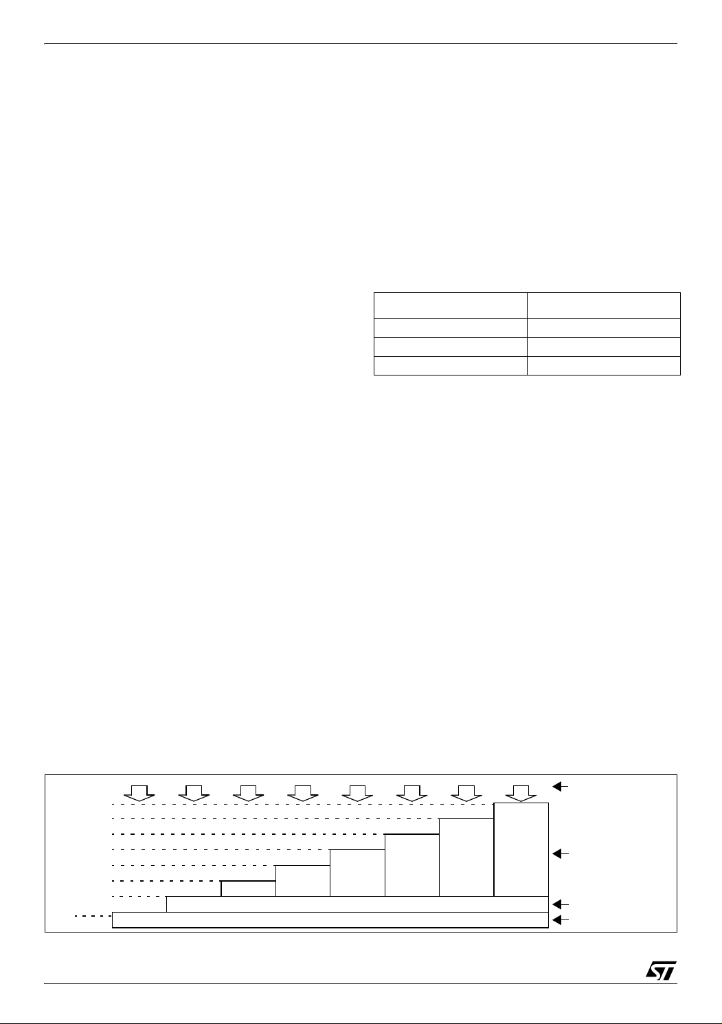
 Loading...
ST ST72321R9, ST72321AR9, ST72321J9, ST72321R7, ST72321AR7 User Manual
...
March 2009 Rev 2 1/193
ST72321Rx
ST72321ARx ST72321Jx
64/44-pin 8-bit MCU with 32 to 60K Flash/ROM, ADC,
five timers, SPI, SCI, I
2
C interface
Features
■ Memories
– 32K to 60K dual voltage High Density Flash
(HDFlash) or ROM with read-out protection
capability. In-Application Programming and
In-Circuit Programming for HDFlash devices
– 1K to 2K RAM
– HDFlash endurance: 100 cycles, data reten-
tion: 40 years at 85°C
■ Clock, Reset And Supply Management
– Enhanced low voltage supervisor (LVD) for
main supply and auxiliar voltage detector
(AVD) with interrupt capability
– Clock sources: crystal/ceramic resonator os-
cillators, internal RC oscillator and bypass for
external clock
– PLL for 2x frequency multiplication
– Four Power Saving Modes: Halt, Active-Halt,
Wait and Slow
■ Interrupt Management
– Nested interrupt controller
– 14 interrupt vectors plus TRAP and RESET
– Top Level Interrupt (TLI) pin on 64-pin devices
– 15/9 external interrupt lines (on 4 vectors)
■ Up to 48 I/O Ports
– 48/32/24 multifunctional bidirectional I/O lines
– 34/22/17 alternate function lines
– 16/12/10 high sink outputs
■ 5 Timers
– Main Clock Controller with: Real time base,
Beep and Clock-out capabilities
– Configurable watchdog timer
– Two 16-bit timers with: 2 input captures, 2 out-
put compares, external clock input on one tim-
er, PWM and pulse generator modes
– 8-bit PWM Auto-reload timer with: 2 input cap-
tures, 4 PWM outputs, output compare and
time base interrupt, external clock with event
detector
■ 3 Communications Interfaces
– SPI synchronous serial interface
– SCI asynchronous serial interface
–I
2
C multimaster interface
■ 1 Analog peripheral
– 10-bit ADC with up to 16 input ports
■ Instruction Set
– 8-bit Data Manipulation
– 63 Basic Instructions
– 17 main Addressing Modes
– 8 x 8 Unsigned Multiply Instruction
■ Development Tools
– Full hardware/software development package
– In-Circuit Testing capability
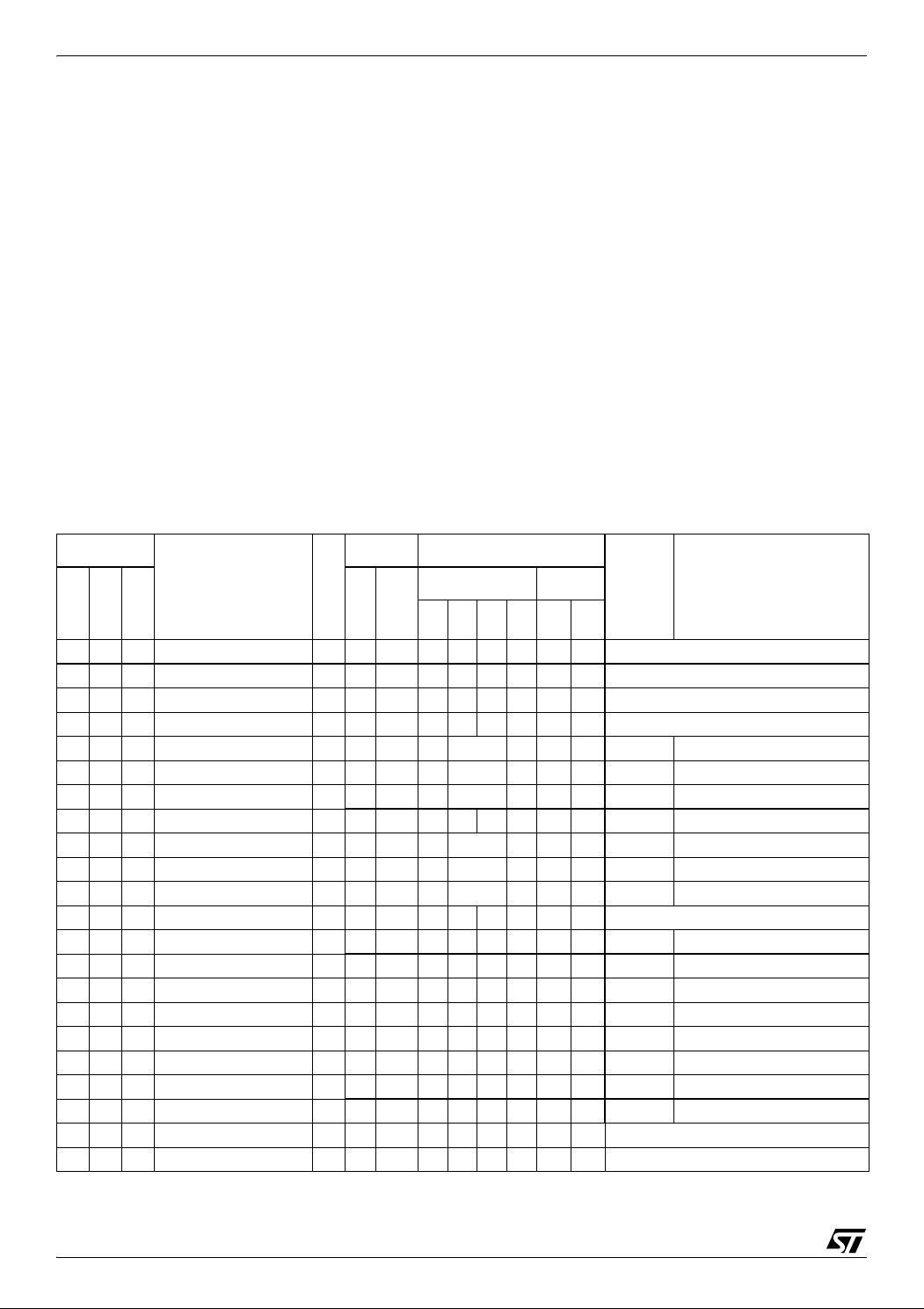
Table 1. Device summary
LQFP64
10 x 10
LQFP64
14 x 14
LQFP44
10 x 10
LQFP32
7 x 7
Features
ST72321R9/ST72321AR9/
ST72321J9
ST72321R7/ST72321AR7/
ST72321J7
ST72321R6/ST72321AR6
Program memory - bytes Flash/ROM 60K Flash/ROM 48K Flash/ROM 32K
RAM (stack) - bytes 2048 (256) 1536 (256) 1024 (256)
Operating Voltage 3.8 to 5.5V
Temp. Range -40 to +125°C, -40 to +85°C
Package LQFP64 14x14 (R), LQFP64 10x10 (AR), LQFP44 10x10 (J)
1

Table of Contents
193
2/193
1 DESCRIPTION . . . . . . . . . . . . . . . . . . . . . . . . . . . . . . . . . . . . . . . . . . . . . . . . . . . . . . . . . . . . . . . 7
2 PIN DESCRIPTION . . . . . . . . . . . . . . . . . . . . . . . . . . . . . . . . . . . . . . . . . . . . . . . . . . . . . . . . . . . . 8
3 REGISTER & MEMORY MAP . . . . . . . . . . . . . . . . . . . . . . . . . . . . . . . . . . . . . . . . . . . . . . . . . . . 14
4 FLASH PROGRAM MEMORY . . . . . . . . . . . . . . . . . . . . . . . . . . . . . . . . . . . . . . . . . . . . . . . . . . 18
4.1 INTRODUCTION . . . . . . . . . . . . . . . . . . . . . . . . . . . . . . . . . . . . . . . . . . . . . . . . . . . . . . . . 18
4.2 MAIN FEATURES . . . . . . . . . . . . . . . . . . . . . . . . . . . . . . . . . . . . . . . . . . . . . . . . . . . . . . . 18
4.3 STRUCTURE . . . . . . . . . . . . . . . . . . . . . . . . . . . . . . . . . . . . . . . . . . . . . . . . . . . . . . . . . . . 18
4.3.1 Read-out Protection . . . . . . . . . . . . . . . . . . . . . . . . . . . . . . . . . . . . . . . . . . . . . . . . 18
4.4 ICC INTERFACE . . . . . . . . . . . . . . . . . . . . . . . . . . . . . . . . . . . . . . . . . . . . . . . . . . . . . . . . 19
4.5 ICP (IN-CIRCUIT PROGRAMMING) . . . . . . . . . . . . . . . . . . . . . . . . . . . . . . . . . . . . . . . . . 20
4.6 IAP (IN-APPLICATION PROGRAMMING) . . . . . . . . . . . . . . . . . . . . . . . . . . . . . . . . . . . . . 20
4.7 RELATED DOCUMENTATION . . . . . . . . . . . . . . . . . . . . . . . . . . . . . . . . . . . . . . . . . . . . . 20
4.7.1 Register Description . . . . . . . . . . . . . . . . . . . . . . . . . . . . . . . . . . . . . . . . . . . . . . . 20
5 CENTRAL PROCESSING UNIT . . . . . . . . . . . . . . . . . . . . . . . . . . . . . . . . . . . . . . . . . . . . . . . . . 21
5.1 INTRODUCTION . . . . . . . . . . . . . . . . . . . . . . . . . . . . . . . . . . . . . . . . . . . . . . . . . . . . . . . . 21
5.2 MAIN FEATURES . . . . . . . . . . . . . . . . . . . . . . . . . . . . . . . . . . . . . . . . . . . . . . . . . . . . . . . 21
5.3 CPU REGISTERS . . . . . . . . . . . . . . . . . . . . . . . . . . . . . . . . . . . . . . . . . . . . . . . . . . . . . . . 21
6 SUPPLY, RESET AND CLOCK MANAGEMENT . . . . . . . . . . . . . . . . . . . . . . . . . . . . . . . . . . . . 24
6.1 PHASE LOCKED LOOP . . . . . . . . . . . . . . . . . . . . . . . . . . . . . . . . . . . . . . . . . . . . . . . . . . 24
6.2 MULTI-OSCILLATOR (MO) . . . . . . . . . . . . . . . . . . . . . . . . . . . . . . . . . . . . . . . . . . . . . . . . 25
6.3 RESET SEQUENCE MANAGER (RSM) . . . . . . . . . . . . . . . . . . . . . . . . . . . . . . . . . . . . . . 26
6.3.1 Introduction . . . . . . . . . . . . . . . . . . . . . . . . . . . . . . . . . . . . . . . . . . . . . . . . . . . . . . 26
6.3.2 Asynchronous External RESET pin . . . . . . . . . . . . . . . . . . . . . . . . . . . . . . . . . . . . 26
6.3.3 External Power-On RESET . . . . . . . . . . . . . . . . . . . . . . . . . . . . . . . . . . . . . . . . . . 27
6.3.4 Internal Low Voltage Detector (LVD) RESET . . . . . . . . . . . . . . . . . . . . . . . . . . . . 27
6.3.5 Internal Watchdog RESET . . . . . . . . . . . . . . . . . . . . . . . . . . . . . . . . . . . . . . . . . . 27
6.4 SYSTEM INTEGRITY MANAGEMENT (SI) . . . . . . . . . . . . . . . . . . . . . . . . . . . . . . . . . . . . 28
6.4.1 Low Voltage Detector (LVD) . . . . . . . . . . . . . . . . . . . . . . . . . . . . . . . . . . . . . . . . . 28
6.4.2 Auxiliary Voltage Detector (AVD) . . . . . . . . . . . . . . . . . . . . . . . . . . . . . . . . . . . . . 29
6.4.3 Low Power Modes . . . . . . . . . . . . . . . . . . . . . . . . . . . . . . . . . . . . . . . . . . . . . . . . 30
6.4.4 Register Description . . . . . . . . . . . . . . . . . . . . . . . . . . . . . . . . . . . . . . . . . . . . . . . 31
7 INTERRUPTS . . . . . . . . . . . . . . . . . . . . . . . . . . . . . . . . . . . . . . . . . . . . . . . . . . . . . . . . . . . . . . . 32
7.1 INTRODUCTION . . . . . . . . . . . . . . . . . . . . . . . . . . . . . . . . . . . . . . . . . . . . . . . . . . . . . . . . 32
7.2 MASKING AND PROCESSING FLOW . . . . . . . . . . . . . . . . . . . . . . . . . . . . . . . . . . . . . . . 32
7.3 INTERRUPTS AND LOW POWER MODES . . . . . . . . . . . . . . . . . . . . . . . . . . . . . . . . . . . 34
7.4 CONCURRENT & NESTED MANAGEMENT . . . . . . . . . . . . . . . . . . . . . . . . . . . . . . . . . . 34
7.5 INTERRUPT REGISTER DESCRIPTION . . . . . . . . . . . . . . . . . . . . . . . . . . . . . . . . . . . . . 35
7.6 EXTERNAL INTERRUPTS . . . . . . . . . . . . . . . . . . . . . . . . . . . . . . . . . . . . . . . . . . . . . . . . 37
7.6.1 I/O Port Interrupt Sensitivity . . . . . . . . . . . . . . . . . . . . . . . . . . . . . . . . . . . . . . . . . . 37
7.7 EXTERNAL INTERRUPT CONTROL REGISTER (EICR) . . . . . . . . . . . . . . . . . . . . . . . . . 39
8 POWER SAVING MODES . . . . . . . . . . . . . . . . . . . . . . . . . . . . . . . . . . . . . . . . . . . . . . . . . . . . . 41
8.1 INTRODUCTION . . . . . . . . . . . . . . . . . . . . . . . . . . . . . . . . . . . . . . . . . . . . . . . . . . . . . . . . 41
8.2 SLOW MODE . . . . . . . . . . . . . . . . . . . . . . . . . . . . . . . . . . . . . . . . . . . . . . . . . . . . . . . . . . . 41
8.3 WAIT MODE . . . . . . . . . . . . . . . . . . . . . . . . . . . . . . . . . . . . . . . . . . . . . . . . . . . . . . . . . . . 42
1

Table of Contents
3/193
8.4 ACTIVE-HALT AND HALT MODES . . . . . . . . . . . . . . . . . . . . . . . . . . . . . . . . . . . . . . . . . . 43
8.4.1 ACTIVE-HALT MODE . . . . . . . . . . . . . . . . . . . . . . . . . . . . . . . . . . . . . . . . . . . . . . 43
8.4.2 HALT MODE . . . . . . . . . . . . . . . . . . . . . . . . . . . . . . . . . . . . . . . . . . . . . . . . . . . . . 44
9 I/O PORTS . . . . . . . . . . . . . . . . . . . . . . . . . . . . . . . . . . . . . . . . . . . . . . . . . . . . . . . . . . . . . . . . . . 46
9.1 INTRODUCTION . . . . . . . . . . . . . . . . . . . . . . . . . . . . . . . . . . . . . . . . . . . . . . . . . . . . . . . . 46
9.2 FUNCTIONAL DESCRIPTION . . . . . . . . . . . . . . . . . . . . . . . . . . . . . . . . . . . . . . . . . . . . . . 46
9.2.1 Input Modes . . . . . . . . . . . . . . . . . . . . . . . . . . . . . . . . . . . . . . . . . . . . . . . . . . . . . . 46
9.2.2 Output Modes . . . . . . . . . . . . . . . . . . . . . . . . . . . . . . . . . . . . . . . . . . . . . . . . . . . . 46
9.2.3 Alternate Functions . . . . . . . . . . . . . . . . . . . . . . . . . . . . . . . . . . . . . . . . . . . . . . . . 46
9.3 I/O PORT IMPLEMENTATION . . . . . . . . . . . . . . . . . . . . . . . . . . . . . . . . . . . . . . . . . . . . . . 49
9.4 LOW POWER MODES . . . . . . . . . . . . . . . . . . . . . . . . . . . . . . . . . . . . . . . . . . . . . . . . . . . 49
9.5 INTERRUPTS . . . . . . . . . . . . . . . . . . . . . . . . . . . . . . . . . . . . . . . . . . . . . . . . . . . . . . . . . . 49
9.5.1 I/O Port Implementation . . . . . . . . . . . . . . . . . . . . . . . . . . . . . . . . . . . . . . . . . . . . . 50
10 ON-CHIP PERIPHERALS . . . . . . . . . . . . . . . . . . . . . . . . . . . . . . . . . . . . . . . . . . . . . . . . . . . . . 52
10.1 WATCHDOG TIMER (WDG) . . . . . . . . . . . . . . . . . . . . . . . . . . . . . . . . . . . . . . . . . . . . . . . 52
10.1.1 Introduction . . . . . . . . . . . . . . . . . . . . . . . . . . . . . . . . . . . . . . . . . . . . . . . . . . . . . . 52
10.1.2 Main Features . . . . . . . . . . . . . . . . . . . . . . . . . . . . . . . . . . . . . . . . . . . . . . . . . . . . 52
10.1.3 Functional Description . . . . . . . . . . . . . . . . . . . . . . . . . . . . . . . . . . . . . . . . . . . . . . 52
10.1.4 How to Program the Watchdog Timeout . . . . . . . . . . . . . . . . . . . . . . . . . . . . . . . . 53
10.1.5 Low Power Modes . . . . . . . . . . . . . . . . . . . . . . . . . . . . . . . . . . . . . . . . . . . . . . . . . 55
10.1.6 Hardware Watchdog Option . . . . . . . . . . . . . . . . . . . . . . . . . . . . . . . . . . . . . . . . . 55
10.1.7 Using Halt Mode with the WDG (WDGHALT option) . . . . . . . . . . . . . . . . . . . . . . . 55
10.1.8 Interrupts . . . . . . . . . . . . . . . . . . . . . . . . . . . . . . . . . . . . . . . . . . . . . . . . . . . . . . . . 55
10.1.9 Register Description . . . . . . . . . . . . . . . . . . . . . . . . . . . . . . . . . . . . . . . . . . . . . . . 55
10.2 MAIN CLOCK CONTROLLER WITH REAL TIME CLOCK AND BEEPER (MCC/RTC) . . 57
10.2.1 Programmable CPU Clock Prescaler . . . . . . . . . . . . . . . . . . . . . . . . . . . . . . . . . . 57
10.2.2 Clock-out Capability . . . . . . . . . . . . . . . . . . . . . . . . . . . . . . . . . . . . . . . . . . . . . . . . 57
10.2.3 Real Time Clock Timer (RTC) . . . . . . . . . . . . . . . . . . . . . . . . . . . . . . . . . . . . . . . . 57
10.2.4 Beeper . . . . . . . . . . . . . . . . . . . . . . . . . . . . . . . . . . . . . . . . . . . . . . . . . . . . . . . . . . 57
10.2.5 Low Power Modes . . . . . . . . . . . . . . . . . . . . . . . . . . . . . . . . . . . . . . . . . . . . . . . . 58
10.2.6 Interrupts . . . . . . . . . . . . . . . . . . . . . . . . . . . . . . . . . . . . . . . . . . . . . . . . . . . . . . . . 58
10.2.7 Register Description . . . . . . . . . . . . . . . . . . . . . . . . . . . . . . . . . . . . . . . . . . . . . . . 58
10.3 PWM AUTO-RELOAD TIMER (ART) . . . . . . . . . . . . . . . . . . . . . . . . . . . . . . . . . . . . . . . . . 60
10.3.1 Introduction . . . . . . . . . . . . . . . . . . . . . . . . . . . . . . . . . . . . . . . . . . . . . . . . . . . . . . 60
10.3.2 Functional Description . . . . . . . . . . . . . . . . . . . . . . . . . . . . . . . . . . . . . . . . . . . . . . 61
10.3.3 Register Description . . . . . . . . . . . . . . . . . . . . . . . . . . . . . . . . . . . . . . . . . . . . . . . 65
10.4 16-BIT TIMER . . . . . . . . . . . . . . . . . . . . . . . . . . . . . . . . . . . . . . . . . . . . . . . . . . . . . . . . . . 69
10.4.1 Introduction . . . . . . . . . . . . . . . . . . . . . . . . . . . . . . . . . . . . . . . . . . . . . . . . . . . . . . 69
10.4.2 Main Features . . . . . . . . . . . . . . . . . . . . . . . . . . . . . . . . . . . . . . . . . . . . . . . . . . . . 69
10.4.3 Functional Description . . . . . . . . . . . . . . . . . . . . . . . . . . . . . . . . . . . . . . . . . . . . . . 69
10.4.4 Low Power Modes . . . . . . . . . . . . . . . . . . . . . . . . . . . . . . . . . . . . . . . . . . . . . . . . 81
10.4.5 Interrupts . . . . . . . . . . . . . . . . . . . . . . . . . . . . . . . . . . . . . . . . . . . . . . . . . . . . . . . 81
10.4.6 Summary of Timer Modes . . . . . . . . . . . . . . . . . . . . . . . . . . . . . . . . . . . . . . . . . . 81
10.4.7 Register Description . . . . . . . . . . . . . . . . . . . . . . . . . . . . . . . . . . . . . . . . . . . . . . . 82
10.5 SERIAL PERIPHERAL INTERFACE (SPI) . . . . . . . . . . . . . . . . . . . . . . . . . . . . . . . . . . . . 88
10.5.1 Introduction . . . . . . . . . . . . . . . . . . . . . . . . . . . . . . . . . . . . . . . . . . . . . . . . . . . . . . 88
10.5.2 Main Features . . . . . . . . . . . . . . . . . . . . . . . . . . . . . . . . . . . . . . . . . . . . . . . . . . . . 88
1

Table of Contents
193
4/193
10.5.3 General Description . . . . . . . . . . . . . . . . . . . . . . . . . . . . . . . . . . . . . . . . . . . . . . . . 88
10.5.4 Clock Phase and Clock Polarity . . . . . . . . . . . . . . . . . . . . . . . . . . . . . . . . . . . . . . 92
10.5.5 Error Flags . . . . . . . . . . . . . . . . . . . . . . . . . . . . . . . . . . . . . . . . . . . . . . . . . . . . . . . 93
10.5.6 Low Power Modes . . . . . . . . . . . . . . . . . . . . . . . . . . . . . . . . . . . . . . . . . . . . . . . . . 95
10.5.7 Interrupts . . . . . . . . . . . . . . . . . . . . . . . . . . . . . . . . . . . . . . . . . . . . . . . . . . . . . . . 95
10.5.8 Register Description . . . . . . . . . . . . . . . . . . . . . . . . . . . . . . . . . . . . . . . . . . . . . . . 96
10.6 SERIAL COMMUNICATIONS INTERFACE (SCI) . . . . . . . . . . . . . . . . . . . . . . . . . . . . . . . 99
10.6.1 Introduction . . . . . . . . . . . . . . . . . . . . . . . . . . . . . . . . . . . . . . . . . . . . . . . . . . . . . . 99
10.6.2 Main Features . . . . . . . . . . . . . . . . . . . . . . . . . . . . . . . . . . . . . . . . . . . . . . . . . . . . 99
10.6.3 General Description . . . . . . . . . . . . . . . . . . . . . . . . . . . . . . . . . . . . . . . . . . . . . . . . 99
10.6.4 Functional Description . . . . . . . . . . . . . . . . . . . . . . . . . . . . . . . . . . . . . . . . . . . . . 101
10.6.5 Low Power Modes . . . . . . . . . . . . . . . . . . . . . . . . . . . . . . . . . . . . . . . . . . . . . . . . 108
10.6.6 Interrupts . . . . . . . . . . . . . . . . . . . . . . . . . . . . . . . . . . . . . . . . . . . . . . . . . . . . . . . 108
10.6.7 Register Description . . . . . . . . . . . . . . . . . . . . . . . . . . . . . . . . . . . . . . . . . . . . . . 109
10.7 I2C BUS INTERFACE (I2C) . . . . . . . . . . . . . . . . . . . . . . . . . . . . . . . . . . . . . . . . . . . . . . . 115
10.7.1 Introduction . . . . . . . . . . . . . . . . . . . . . . . . . . . . . . . . . . . . . . . . . . . . . . . . . . . . . 115
10.7.2 Main Features . . . . . . . . . . . . . . . . . . . . . . . . . . . . . . . . . . . . . . . . . . . . . . . . . . . 115
10.7.3 General Description . . . . . . . . . . . . . . . . . . . . . . . . . . . . . . . . . . . . . . . . . . . . . . . 115
10.7.4 Functional Description . . . . . . . . . . . . . . . . . . . . . . . . . . . . . . . . . . . . . . . . . . . . . 117
10.7.5 Low Power Modes . . . . . . . . . . . . . . . . . . . . . . . . . . . . . . . . . . . . . . . . . . . . . . . . 121
10.7.6 Interrupts . . . . . . . . . . . . . . . . . . . . . . . . . . . . . . . . . . . . . . . . . . . . . . . . . . . . . . . 121
10.7.7 Register Description . . . . . . . . . . . . . . . . . . . . . . . . . . . . . . . . . . . . . . . . . . . . . . 122
10.8 10-BIT A/D CONVERTER (ADC) . . . . . . . . . . . . . . . . . . . . . . . . . . . . . . . . . . . . . . . . . . . 128
10.8.1 Introduction . . . . . . . . . . . . . . . . . . . . . . . . . . . . . . . . . . . . . . . . . . . . . . . . . . . . . 128
10.8.2 Main Features . . . . . . . . . . . . . . . . . . . . . . . . . . . . . . . . . . . . . . . . . . . . . . . . . . . 128
10.8.3 Functional Description . . . . . . . . . . . . . . . . . . . . . . . . . . . . . . . . . . . . . . . . . . . . . 129
10.8.4 Low Power Modes . . . . . . . . . . . . . . . . . . . . . . . . . . . . . . . . . . . . . . . . . . . . . . . . 129
10.8.5 Interrupts . . . . . . . . . . . . . . . . . . . . . . . . . . . . . . . . . . . . . . . . . . . . . . . . . . . . . . . 129
10.8.6 Register Description . . . . . . . . . . . . . . . . . . . . . . . . . . . . . . . . . . . . . . . . . . . . . . 130
11 INSTRUCTION SET . . . . . . . . . . . . . . . . . . . . . . . . . . . . . . . . . . . . . . . . . . . . . . . . . . . . . . . . 132
11.1 CPU ADDRESSING MODES . . . . . . . . . . . . . . . . . . . . . . . . . . . . . . . . . . . . . . . . . . . . . . 132
11.1.1 Inherent . . . . . . . . . . . . . . . . . . . . . . . . . . . . . . . . . . . . . . . . . . . . . . . . . . . . . . . . 133
11.1.2 Immediate . . . . . . . . . . . . . . . . . . . . . . . . . . . . . . . . . . . . . . . . . . . . . . . . . . . . . . 133
11.1.3 Direct . . . . . . . . . . . . . . . . . . . . . . . . . . . . . . . . . . . . . . . . . . . . . . . . . . . . . . . . . . 133
11.1.4 Indexed (No Offset, Short, Long) . . . . . . . . . . . . . . . . . . . . . . . . . . . . . . . . . . . . . 133
11.1.5 Indirect (Short, Long) . . . . . . . . . . . . . . . . . . . . . . . . . . . . . . . . . . . . . . . . . . . . . . 133
11.1.6 Indirect Indexed (Short, Long) . . . . . . . . . . . . . . . . . . . . . . . . . . . . . . . . . . . . . . . 134
11.1.7 Relative mode (Direct, Indirect) . . . . . . . . . . . . . . . . . . . . . . . . . . . . . . . . . . . . . . 134
11.2 INSTRUCTION GROUPS . . . . . . . . . . . . . . . . . . . . . . . . . . . . . . . . . . . . . . . . . . . . . . . . 135
12 ELECTRICAL CHARACTERISTICS . . . . . . . . . . . . . . . . . . . . . . . . . . . . . . . . . . . . . . . . . . . . 138
12.1 PARAMETER CONDITIONS . . . . . . . . . . . . . . . . . . . . . . . . . . . . . . . . . . . . . . . . . . . . . . 138
12.1.1 Minimum and Maximum values . . . . . . . . . . . . . . . . . . . . . . . . . . . . . . . . . . . . . . 138
12.1.2 Typical values . . . . . . . . . . . . . . . . . . . . . . . . . . . . . . . . . . . . . . . . . . . . . . . . . . . 138
12.1.3 Typical curves . . . . . . . . . . . . . . . . . . . . . . . . . . . . . . . . . . . . . . . . . . . . . . . . . . . 138
12.1.4 Loading capacitor . . . . . . . . . . . . . . . . . . . . . . . . . . . . . . . . . . . . . . . . . . . . . . . . 138
12.1.5 Pin input voltage . . . . . . . . . . . . . . . . . . . . . . . . . . . . . . . . . . . . . . . . . . . . . . . . . 138
12.2 ABSOLUTE MAXIMUM RATINGS . . . . . . . . . . . . . . . . . . . . . . . . . . . . . . . . . . . . . . . . . . 139

Table of Contents
5/193
12.2.1 Voltage Characteristics . . . . . . . . . . . . . . . . . . . . . . . . . . . . . . . . . . . . . . . . . . . . 139
12.2.2 Current Characteristics . . . . . . . . . . . . . . . . . . . . . . . . . . . . . . . . . . . . . . . . . . . . 139
12.2.3 Thermal Characteristics . . . . . . . . . . . . . . . . . . . . . . . . . . . . . . . . . . . . . . . . . . . 140
12.3 OPERATING CONDITIONS . . . . . . . . . . . . . . . . . . . . . . . . . . . . . . . . . . . . . . . . . . . . . . . 140
12.3.1 General Operating Conditions . . . . . . . . . . . . . . . . . . . . . . . . . . . . . . . . . . . . . . . 140
12.3.2 Operating Conditions with Low Voltage Detector (LVD) . . . . . . . . . . . . . . . . . . . 141
12.3.3 Auxiliary Voltage Detector (AVD) Thresholds . . . . . . . . . . . . . . . . . . . . . . . . . . . 141
12.3.4 External Voltage Detector (EVD) Thresholds . . . . . . . . . . . . . . . . . . . . . . . . . . . 141
12.4 SUPPLY CURRENT CHARACTERISTICS . . . . . . . . . . . . . . . . . . . . . . . . . . . . . . . . . . . 142
12.4.1 CURRENT CONSUMPTION . . . . . . . . . . . . . . . . . . . . . . . . . . . . . . . . . . . . . 142
12.4.2 Supply and Clock Managers . . . . . . . . . . . . . . . . . . . . . . . . . . . . . . . . . . . . . . . . 144
12.4.3 On-Chip Peripherals . . . . . . . . . . . . . . . . . . . . . . . . . . . . . . . . . . . . . . . . . . . . . . 145
12.5 CLOCK AND TIMING CHARACTERISTICS . . . . . . . . . . . . . . . . . . . . . . . . . . . . . . . . . . 146
12.5.1 General Timings . . . . . . . . . . . . . . . . . . . . . . . . . . . . . . . . . . . . . . . . . . . . . . . . . 146
12.5.2 External Clock Source . . . . . . . . . . . . . . . . . . . . . . . . . . . . . . . . . . . . . . . . . . . . 146
12.5.3 Crystal and Ceramic Resonator Oscillators . . . . . . . . . . . . . . . . . . . . . . . . . . . . . 147
12.5.4 RC Oscillators . . . . . . . . . . . . . . . . . . . . . . . . . . . . . . . . . . . . . . . . . . . . . . . . . . . 150
12.5.5 PLL Characteristics . . . . . . . . . . . . . . . . . . . . . . . . . . . . . . . . . . . . . . . . . . . . . . . 151
12.6 MEMORY CHARACTERISTICS . . . . . . . . . . . . . . . . . . . . . . . . . . . . . . . . . . . . . . . . . . . 152
12.6.1 RAM and Hardware Registers . . . . . . . . . . . . . . . . . . . . . . . . . . . . . . . . . . . . . . 152
12.6.2 FLASH Memory . . . . . . . . . . . . . . . . . . . . . . . . . . . . . . . . . . . . . . . . . . . . . . . . . 152
12.7 EMC CHARACTERISTICS . . . . . . . . . . . . . . . . . . . . . . . . . . . . . . . . . . . . . . . . . . . . . . . 153
12.7.1 Functional EMS (Electro Magnetic Susceptibility) . . . . . . . . . . . . . . . . . . . . . . . . 153
12.7.2 Electro Magnetic Interference (EMI) . . . . . . . . . . . . . . . . . . . . . . . . . . . . . . . . . . 154
12.7.3 Absolute Maximum Ratings (Electrical Sensitivity) . . . . . . . . . . . . . . . . . . . . . . . 155
12.8 I/O PORT PIN CHARACTERISTICS . . . . . . . . . . . . . . . . . . . . . . . . . . . . . . . . . . . . . . . . 156
12.8.1 General Characteristics . . . . . . . . . . . . . . . . . . . . . . . . . . . . . . . . . . . . . . . . . . . . 156
12.8.2 Output Driving Current . . . . . . . . . . . . . . . . . . . . . . . . . . . . . . . . . . . . . . . . . . . . . 157
12.9 CONTROL PIN CHARACTERISTICS . . . . . . . . . . . . . . . . . . . . . . . . . . . . . . . . . . . . . . . 159
12.9.1 Asynchronous RESET Pin . . . . . . . . . . . . . . . . . . . . . . . . . . . . . . . . . . . . . . . . . . 159
12.9.2 ICCSEL/VPP Pin . . . . . . . . . . . . . . . . . . . . . . . . . . . . . . . . . . . . . . . . . . . . . . . . . 161
12.10TIMER PERIPHERAL CHARACTERISTICS . . . . . . . . . . . . . . . . . . . . . . . . . . . . . . . . . 162
12.10.1 8-Bit PWM-ART Auto-Reload Timer . . . . . . . . . . . . . . . . . . . . . . . . . . . . . . . . . . 162
12.10.2 16-Bit Timer . . . . . . . . . . . . . . . . . . . . . . . . . . . . . . . . . . . . . . . . . . . . . . . . . . . . 162
12.11COMMUNICATION INTERFACE CHARACTERISTICS . . . . . . . . . . . . . . . . . . . . . . . . 163
12.11.1 SPI - Serial Peripheral Interface . . . . . . . . . . . . . . . . . . . . . . . . . . . . . . . . . . . . . 163
12.11.2 I2C - Inter IC Control Interface . . . . . . . . . . . . . . . . . . . . . . . . . . . . . . . . . . . . . . 165
12.1210-BIT ADC CHARACTERISTICS . . . . . . . . . . . . . . . . . . . . . . . . . . . . . . . . . . . . . . . . . 167
12.12.1 Analog Power Supply and Reference Pins . . . . . . . . . . . . . . . . . . . . . . . . . . . . . 169
12.12.2 General PCB Design Guidelines . . . . . . . . . . . . . . . . . . . . . . . . . . . . . . . . . . . . . 169
12.12.3 ADC Accuracy . . . . . . . . . . . . . . . . . . . . . . . . . . . . . . . . . . . . . . . . . . . . . . . . . . . 170
13 PACKAGE CHARACTERISTICS . . . . . . . . . . . . . . . . . . . . . . . . . . . . . . . . . . . . . . . . . . . . . . 171
13.1 PACKAGE MECHANICAL DATA . . . . . . . . . . . . . . . . . . . . . . . . . . . . . . . . . . . . . . . . . . . 171
13.2 THERMAL CHARACTERISTICS . . . . . . . . . . . . . . . . . . . . . . . . . . . . . . . . . . . . . . . . . . 173
13.3 SOLDERING AND GLUEABILITY INFORMATION . . . . . . . . . . . . . . . . . . . . . . . . . . . . . 174
14 ST72321 DEVICE CONFIGURATION AND ORDERING INFORMATION . . . . . . . . . . . . . . . 175

Table of Contents
193
6/193
14.1 FLASH OPTION BYTES . . . . . . . . . . . . . . . . . . . . . . . . . . . . . . . . . . . . . . . . . . . . . . . . . 175
14.2 DEVICE ORDERING INFORMATION AND TRANSFER OF CUSTOMER CODE . . . . . 177
14.3 DEVELOPMENT TOOLS . . . . . . . . . . . . . . . . . . . . . . . . . . . . . . . . . . . . . . . . . . . . . . . . . 181
14.3.1 Starter kits . . . . . . . . . . . . . . . . . . . . . . . . . . . . . . . . . . . . . . . . . . . . . . . . . . . . . . 181
14.3.2 Development and debugging tools . . . . . . . . . . . . . . . . . . . . . . . . . . . . . . . . . . . 181
14.3.3 Programming tools . . . . . . . . . . . . . . . . . . . . . . . . . . . . . . . . . . . . . . . . . . . . . . . 181
14.3.4 Socket and Emulator Adapter Information . . . . . . . . . . . . . . . . . . . . . . . . . . . . . . 182
14.4 ST7 APPLICATION NOTES . . . . . . . . . . . . . . . . . . . . . . . . . . . . . . . . . . . . . . . . . . . . . . 183
15 KNOWN LIMITATIONS . . . . . . . . . . . . . . . . . . . . . . . . . . . . . . . . . . . . . . . . . . . . . . . . . . . . . . 186
15.1 ALL FLASH AND ROM DEVICES . . . . . . . . . . . . . . . . . . . . . . . . . . . . . . . . . . . . . . . . . . 186
15.1.1 External RC option . . . . . . . . . . . . . . . . . . . . . . . . . . . . . . . . . . . . . . . . . . . . . . . 186
15.1.2 Safe Connection of OSC1/OSC2 Pins . . . . . . . . . . . . . . . . . . . . . . . . . . . . . . . . 186
15.1.3 Reset pin protection with LVD Enabled . . . . . . . . . . . . . . . . . . . . . . . . . . . . . . . . 186
15.1.4 Unexpected Reset Fetch . . . . . . . . . . . . . . . . . . . . . . . . . . . . . . . . . . . . . . . . . . . 186
15.1.5 External interrupt missed . . . . . . . . . . . . . . . . . . . . . . . . . . . . . . . . . . . . . . . . . . . 186
15.1.6 Clearing active interrupts outside interrupt routine . . . . . . . . . . . . . . . . . . . . . . . 187
15.1.7 SCI Wrong Break duration . . . . . . . . . . . . . . . . . . . . . . . . . . . . . . . . . . . . . . . . . . 189
15.1.8 16-bit Timer PWM Mode . . . . . . . . . . . . . . . . . . . . . . . . . . . . . . . . . . . . . . . . . . . 189
15.1.9 TIMD set simultaneously with OC interrupt . . . . . . . . . . . . . . . . . . . . . . . . . . . . . 189
15.1.10 I2C Multimaster . . . . . . . . . . . . . . . . . . . . . . . . . . . . . . . . . . . . . . . . . . . . . . . . . . 189
15.2 ALL FLASH DEVICES . . . . . . . . . . . . . . . . . . . . . . . . . . . . . . . . . . . . . . . . . . . . . . . . . . . 189
15.2.1 Internal RC Oscillator with LVD . . . . . . . . . . . . . . . . . . . . . . . . . . . . . . . . . . . . . . 189
15.3 LIMITATIONS SPECIFIC TO REV Q AND REV S FLASH DEVICES . . . . . . . . . . . . . . . 189
15.3.1 ADC Accuracy . . . . . . . . . . . . . . . . . . . . . . . . . . . . . . . . . . . . . . . . . . . . . . . . . . . 189
15.4 LIMITATIONS SPECIFIC TO ROM DEVICES . . . . . . . . . . . . . . . . . . . . . . . . . . . . . . . . . 190
15.4.1 LVD Operation . . . . . . . . . . . . . . . . . . . . . . . . . . . . . . . . . . . . . . . . . . . . . . . . . . . 190
15.4.2 LVD Startup behaviour . . . . . . . . . . . . . . . . . . . . . . . . . . . . . . . . . . . . . . . . . . . . 191
15.4.3 AVD not supported . . . . . . . . . . . . . . . . . . . . . . . . . . . . . . . . . . . . . . . . . . . . . . . 191
15.4.4 Internal RC oscillator operation . . . . . . . . . . . . . . . . . . . . . . . . . . . . . . . . . . . . . . 191
15.4.5 External clock source with PLL . . . . . . . . . . . . . . . . . . . . . . . . . . . . . . . . . . . . . . 191
15.4.6 Pull-up not present on PE2 . . . . . . . . . . . . . . . . . . . . . . . . . . . . . . . . . . . . . . . . . 191
15.4.7 Read-out protection with LVD . . . . . . . . . . . . . . . . . . . . . . . . . . . . . . . . . . . . . . . 191
15.4.8 Safe Connection of OSC1/OSC2 Pins . . . . . . . . . . . . . . . . . . . . . . . . . . . . . . . . 191
16 REVISION HISTORY . . . . . . . . . . . . . . . . . . . . . . . . . . . . . . . . . . . . . . . . . . . . . . . . . . . . . . . . 192
ST72321Rx ST72321ARx ST72321Jx
7/193
1 DESCRIPTION
The ST72F321 Flash and ST72321 ROM devices
are members of the ST7 microcontroller family de-
signed for mid-range applications.
All devices are based on a common industry-
standard 8-bit core, featuring an enhanced instruc-
tion set and are available with Flash or ROM pro-
gram memory. The ST7 family architecture offers
both power and flexibility to software developers,
enabling the design of highly efficient and compact
application code.
The on-chip peripherals include an A/D converter,
a PWM Autoreload timer, 2 general purpose tim-
ers, I
2
C bus, SPI interface and an SCI interface.
For power economy, microcontroller can switch
dynamically into WAIT, SLOW, ACTIVE-HALT or
HALT mode when the application is in idle or
stand-by state.
Typical applications are consumer, home, office
and industrial products.
Related Documentation
AN1131: Migrating applications from ST72511/
311/314 to ST72521/321/324
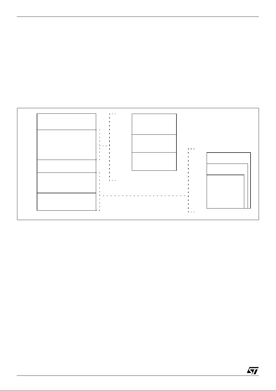
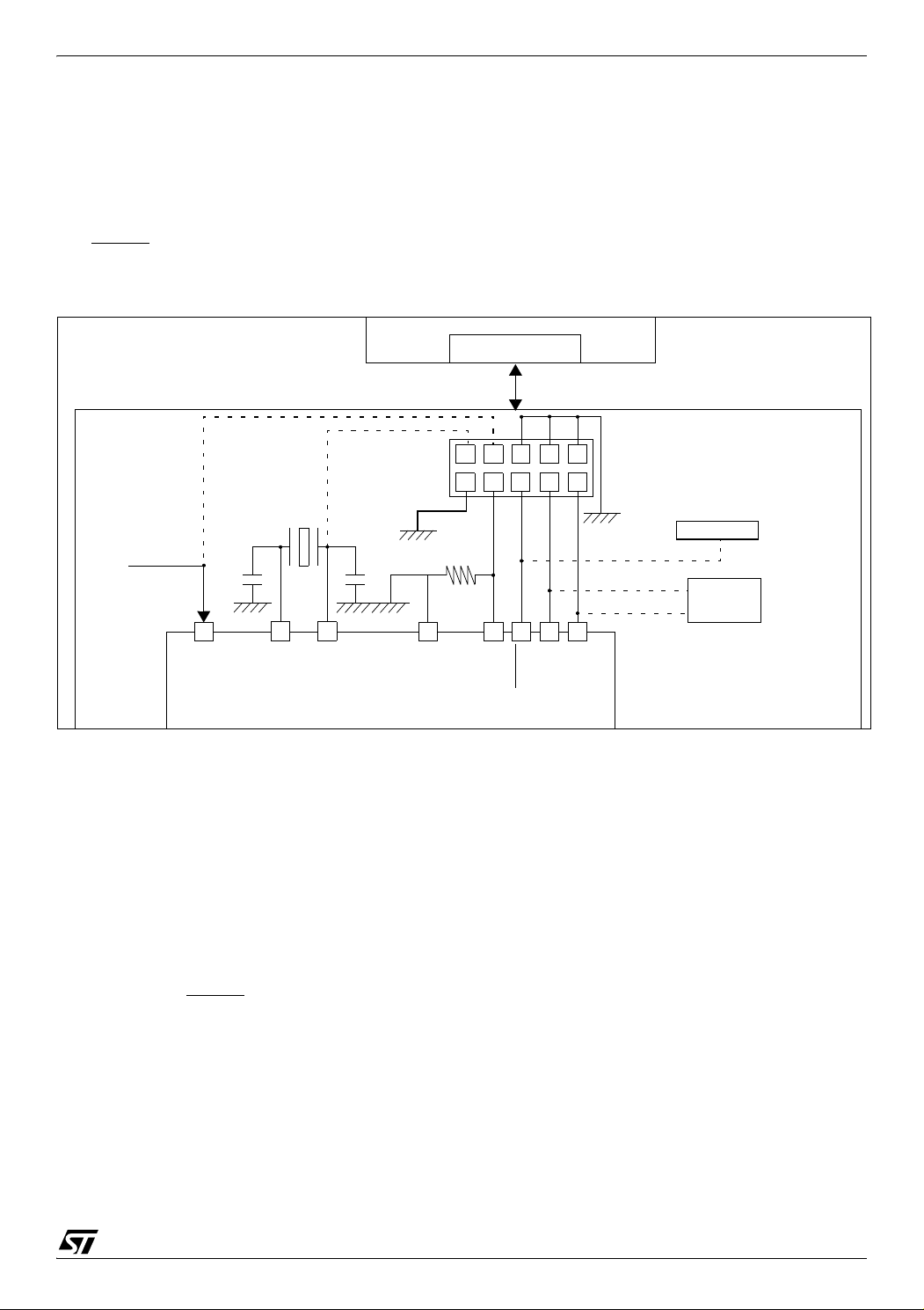
Figure 1. Device Block Diagram
8-BIT CORE
ALU
ADDRESS AND DATA BUS
OSC1
V
PP
CONTROL
PROGRAM
(32K - 60K Bytes)
V
DD
RESET
PORT F
PF7:0
(8-bits)
TIMER A
BEEP
PORT A
RAM
(1024 - 2048 Bytes)
PORT C
10-BIT ADC
V
AREF
V
SSA
PORT B
PB7:0
(8-bits)
PWM ART
PORT E
PE7:0
(8-bits)
SCI
TIMER B
PA7:0
(8-bits)
PORT D
PD7:0
(8-bits)
SPI
PC7:0
(8-bits)
V
SS
WATCHDOG
TLI
OSC
LVD
OSC2
MEMORY
MCC/RTC/BEEP
EVD
AVD
I2C
ST72321Rx ST72321ARx ST72321Jx
8/193
2 PIN DESCRIPTION
Figure 2. 64-Pin LQFP 14x14 and 10x10 Package Pinout
V
AREF
V
SSA
V
DD_3
V
SS_3
MCO / AIN8 / PF0
BEEP / (HS) PF1
(HS) PF2
OCMP2_A / AIN9 / PF3
OCMP1_A / AIN10 / PF4
ICAP2_A / AIN11 / PF5
ICAP1_A / (HS) PF6
EXTCLK_A / (HS) PF7
AIN4 / PD4
AIN5 / PD5
AIN6 / PD6
AIN7 / PD7
64 63 62 61 60 59 58 57 56 55 54 53 52 51 50 49
48
47
46
45
44
43
42
41
40
39
38
37
36
35
34
33
17 18 19 20 21 22 23 24 29 30 31 3225 26 27 28
1
2
3
4
5
6
7
8
9
10
11
12
13
14
15
16
ei2
ei3
ei0
ei1
PWM3 / PB0
PWM2 / PB1
PWM1 / PB2
PWM0 / PB3
ARTCLK / (HS) PB4
ARTIC1 / PB5
ARTIC2 / PB6
PB7
AIN0 / PD0
AIN1 / PD1
AIN2 / PD2
AIN3 / PD3
(HS) PE4
(HS) PE5
(HS) PE6
(HS) PE7
PA1
PA0
PC7 / SS / AIN15
PC6 / SCK / ICCCLK
PC5 / MOSI / AIN14
PC4 / MISO / ICCDATA
PC3 (HS) / ICAP1_B
PC2 (HS) / ICAP2_B
PC1 / OCMP1_B / AIN13
PC0 / OCMP2_B / AIN12
V
SS_0
V
DD_0
V
SS_1
V
DD_1
PA3 (HS)
PA2
V
DD
_2
OSC1
OSC2
V
SS
_2
TLI
EVD
RESET
V
PP
/ ICCSEL
PA7 (HS) / SCLI
PA6 (HS) / SDAI
PA5 (HS)
PA4 (HS)
PE3
PE2
PE1 / RDI
PE0 / TDO
(HS) 20mA high sink capability
eix associated external interrupt vector
ST72321Rx ST72321ARx ST72321Jx
9/193
Figure 3. 44-Pin LQFP Package Pinout
MCO / AIN8 / PF0
BEEP / (HS) PF1
(HS) PF2
OCMP1_A / AIN10 / PF4
ICAP1_A / (HS) PF6
EXTCLK_A / (HS) PF7
V
DD_0
V
SS_0
AIN5 / PD5
V
AREF
V
SSA
44 43 42 41 40 39 38 37 36 35 34
33
32
31
30
29
28
27
26
25
24
23
12 13 14 15 16 17 18 19 20 21 22
1
2
3
4
5
6
7
8
9
10
11
ei2
ei3
ei0
ei1
PB3
(HS) PB4
AIN0 / PD0
AIN1 / PD1
AIN2 / PD2
AIN3 / PD3
AIN4 / PD4
RDI / PE1
PB0
PB1
PB2
PC6 / SCK / ICCCLK
PC5 / MOSI / AIN14
PC4 / MISO / ICCDATA
PC3 (HS) / ICAP1_B
PC2 (HS) / ICAP2_B
PC1 / OCMP1_B / AIN13
PC0 / OCMP2_B / AIN12
V
SS_1
V
DD_1
PA3 (HS)
PC7 / SS
/ AIN15
V
SS
_2
RESET
V
PP
/ ICCSEL
PA7 (HS)/ SCLI
PA6 (HS) / SDAI
PA5 (HS)
PA4 (HS)
PE0 / TDO
V
DD
_2
OSC1
OSC2
eix associated external interrupt vector
(HS) 20mA high sink capability
ST72321Rx ST72321ARx ST72321Jx
10/193
PIN DESCRIPTION (Cont’d)
For external pin connection guidelines, refer to See “ELECTRICAL CHARACTERISTICS” on page 138.
Legend / Abbreviations for Table 2 :
Type: I = input, O = output, S = supply
Input level: A = Dedicated analog input
In/Output level: C = CMOS 0.3V
DD
/0.7V
DD
C
T
= CMOS 0.3V
DD
/0.7V
DD
with input trigger
T
T
= TTL 0.8V / 2V with Schmitt trigger
Output level: HS = 20mA high sink (on N-buffer only)
Port and control configuration:
– Input: float = floating, wpu = weak pull-up, int = interrupt
1)
, ana = analog
– Output: OD = open drain
2)
, PP = push-pull
Refer to “I/O PORTS” on page 46 for more details on the software configuration of the I/O ports.
The RESET configuration of each pin is shown in bold. This configuration is valid as long as the device is
in reset state.
Table 2. Device Pin Description
Pin n°
Pin Name
Type
Level Port
Main
function
(after
reset)
Alternate function
LQFP64
LQFP44
LQFP32
Input
Output
Input Output
float
wpu
int
ana
OD
PP
1 - - PE4 (HS) I/O C
T
HS X XXXPort E4
2 - - PE5 (HS) I/O C
T
HS X XXXPort E5
3 - - PE6 (HS) I/O C
T
HS X XXXPort E6
4 - - PE7 (HS) I/O C
T
HS X XXXPort E7
5 2 28 PB0/PWM3 I/O C
T
X ei2 X X Port B0 PWM Output 3
6 3 - PB1/PWM2 I/O C
T
X ei2 X X Port B1 PWM Output 2
7 4 - PB2/PWM1 I/O C
T
X ei2 X X Port B2 PWM Output 1
8 5 29 PB3/PWM0 I/O C
T
X ei2 X X Port B3 PWM Output 0
9 6 30 PB4 (HS)/ARTCLK I/O C
T
HS X ei3 X X Port B4 PWM-ART External Clock
10 - - PB5 / ARTIC1 I/O C
T
X ei3 X X Port B5 PWM-ART Input Capture 1
11 - - PB6 / ARTIC2 I/O C
T
X ei3 X X Port B6 PWM-ART Input Capture 2
12 - - PB7 I/O C
T
X ei3 X X Port B7
13 7 31 PD0/AIN0 I/O C
T
X X X X X Port D0 ADC Analog Input 0
14 8 32 PD1/AIN1 I/O C
T
X X X X X Port D1 ADC Analog Input 1
15 9 - PD2/AIN2 I/O C
T
X X X X X Port D2 ADC Analog Input 2
16 10 - PD3/AIN3 I/O C
T
X X X X X Port D3 ADC Analog Input 3
17 11 - PD4/AIN4 I/O C
T
X X X X X Port D4 ADC Analog Input 4
18 12 - PD5/AIN5 I/O C
T
X X X X X Port D5 ADC Analog Input 5
19 - - PD6/AIN6 I/O C
T
X X X X X Port D6 ADC Analog Input 6
20 - - PD7/AIN7 I/O C
T
X X X X X Port D7 ADC Analog Input 7
21 13 1 V
AREF
I Analog Reference Voltage for ADC
22 14 2 V
SSA
S Analog Ground Voltage

ST72321Rx ST72321ARx ST72321Jx
11/193
23 - - V
DD_3
S Digital Main Supply Voltage
24 - - V
SS_3
S Digital Ground Voltage
25 15 3 PF0/MCO/AIN8 I/O C
T
X ei1 X X X Port F0
Main clock
out (f
OSC
/2)
ADC Ana-
log
Input 8
26 16 4 PF1 (HS)/BEEP I/O C
T
HS X ei1 X X Port F1 Beep signal output
27 17 - PF2 (HS) I/O C
T
HS X ei1 X X Port F2
28 - - PF3/OCMP2_A/AIN9 I/O C
T
X XXXXPort F3
Timer A Out-
put Compare
2
ADC Ana-
log
Input 9
29 18 5
PF4/OCMP1_A/
AIN10
I/O C
T
X XXXXPort F4
Timer A Out-
put Compare
1
ADC Ana-
log
Input 10
30 - - PF5/ICAP2_A/AIN11 I/O C
T
X XXXXPort F5
Timer A Input
Capture 2
ADC Ana-
log
Input 11
31 19 6 PF6 (HS)/ICAP1_A I/O C
T
HS X X X X Port F6 Timer A Input Capture 1
32 20 7 PF7 (HS)/EXTCLK_A I/O C
T
HS X XXXPort F7
Timer A External Clock
Source
33 21 - V
DD_0
S Digital Main Supply Voltage
34 22 - V
SS_0
S Digital Ground Voltage
35 23 8
PC0/OCMP2_B/
AIN12
I/O C
T
X XXXXPort C0
Timer B Out-
put Compare
2
ADC Ana-
log
Input 12
36 24 9
PC1/OCMP1_B/
AIN13
I/O C
T
X XXXXPort C1
Timer B Out-
put Compare
1
ADC Ana-
log
Input 13
37 25 10 PC2 (HS)/ICAP2_B I/O C
T
HS X X X X Port C2 Timer B Input Capture 2
38 26 11 PC3 (HS)/ICAP1_B I/O C
T
HS X X X X Port C3 Timer B Input Capture 1
39 27 12 PC4/MISO/ICCDATA I/O C
T
X XXXPort C4
SPI Master In
/ Slave Out
Data
ICC Data
Input
40 28 13 PC5/MOSI/AIN14 I/O C
T
X XXXXPort C5
SPI Master
Out / Slave In
Data
ADC Ana-
log
Input 14
41 29 29 PC6/SCK/ICCCLK I/O C
T
X XXXPort C6
SPI Serial
Clock
ICC Clock
Output
Caution: Negative cur-
rent injection not al-
lowed on this pin
42 30 15 PC7/SS/AIN15 I/O C
T
X XXXXPort C7
SPI Slave Se-
lect (active
low)
ADC Ana-
log
Input 15
43 - - PA0 I/O C
T
X ei0 X X Port A0
44 - - PA1 I/O C
T
X ei0 X X Port A1
Pin n°
Pin Name
Type
Level Port
Main
function
(after
reset)
Alternate function
LQFP64
LQFP44
LQFP32
Input
Output
Input Output
float
wpu
int
ana
OD
PP
ST72321Rx ST72321ARx ST72321Jx
12/193
Notes:
1. In the interrupt input column, “eiX” defines the associated external interrupt vector. If the weak pull-up
column (wpu) is merged with the interrupt column (int), then the I/O configuration is pull-up interrupt input,
else the configuration is floating interrupt input.
2. In the open drain output column, “T” defines a true open drain I/O (P-Buffer and protection diode to V
DD
are not implemented). See See “I/O PORTS” on page 46. and Section 12.8 I/O PORT PIN CHARACTER-
45 - - PA2 I/O C
T
X ei0 X X Port A2
46 31 16 PA3 (HS) I/O C
T
HS X ei0 X X Port A3
47 32 - V
DD_1
S Digital Main Supply Voltage
48 33 - V
SS_1
S Digital Ground Voltage
49 34 17 PA4 (HS) I/O C
T
HS X XXXPort A4
50 35 - PA5 (HS) I/O C
T
HS X XXXPort A5
51 36 18 PA6 (HS)/SDAI I/O C
T
HS X TPort A6 I
2
C Data
1)
52 37 19 PA7 (HS)/SCLI I/O C
T
HS X TPort A7 I
2
C Clock
1)
53 38 20 V
PP
/ ICCSEL I
Must be tied low. In flash program-
ming mode, this pin acts as the pro-
gramming voltage input V
PP
. See
Section 12.9.2 for more details. High
voltage must not be applied to ROM
devices
54 39 21 RESET
I/O C
T
Top priority non maskable interrupt.
55 - - EVD External voltage detector
56 - - TLI I C
T
X Top level interrupt input pin
57 40 22 V
SS_2
S Digital Ground Voltage
58 41 23 OSC2
3)
I/O Resonator oscillator inverter output
59 42 24 OSC1
3)
I
External clock input or Resonator os-
cillator inverter input
60 43 25 V
DD_2
S Digital Main Supply Voltage
61 44 26 PE0/TDO I/O C
T
X X X X Port E0 SCI Transmit Data Out
62 1 27 PE1/RDI I/O C
T
X X X X Port E1 SCI Receive Data In
63 - -
PE2 (Flash device)
I/O C
T
X
Port E2
Caution: In Flash devices this port is
always input with weak pull-up.
PE2 (ROM device) X XX
Port E2
Caution: In ROM devices, no weak
pull-up present on this port.
In LQFP44 this pin is not connected to
an internal pull-up like other unbond-
ed pins (See note 4). It is recommend-
ed to configure it as output push pull
to avoid added current consumption.
64 - - PE3 I/O C
T
X XXXPort E3
Pin n°
Pin Name
Type
Level Port
Main
function
(after
reset)
Alternate function
LQFP64
LQFP44
LQFP32
Input
Output
Input Output
float
wpu
int
ana
OD
PP

ST72321Rx ST72321ARx ST72321Jx
13/193
ISTICS for more details.
3. OSC1 and OSC2 pins connect a crystal/ceramic resonator, or an external source to the on-chip oscil-
lator; see Section 1 DESCRIPTION and Section 12.5 CLOCK AND TIMING CHARACTERISTICS for
more details.
4. On the chip, each I/O port may have up to 8 pads:
– ads that are not bonded to external pins are forced by hardware in input pull-up configuration after reset.
The configuration of these pads must be kept at reset state to avoid added current consumption.
5. Pull-up always activated on PE2 see limitation Section 15.4.6.
6. It is mandatory to connect all available V
DD
and V
REF
pins to the supply voltage and all V
SS
and V
SSA
pins to ground.
ST72321Rx ST72321ARx ST72321Jx
14/193
3 REGISTER & MEMORY MAP
As shown in Figure 4, the MCU is capable of ad-
dressing 64K bytes of memories and I/O registers.
The available memory locations consist of 128
bytes of register locations, up to 2Kbytes of RAM
and up to 60Kbytes of user program memory. The
RAM space includes up to 256 bytes for the stack
from 0100h to 01FFh.
The highest address bytes contain the user reset
and interrupt vectors.
IMPORTANT: Memory locations marked as “Re-
served” must never be accessed. Accessing a re-
seved area can have unpredictable effects on the
device.
Related Documentation
AN 985: Executing Code in ST7 RAM
Figure 4. Memory Map
0000h
RAM
Program Memory
(60K, 48K or 32K)
Interrupt & Reset Vectors
HW Registers
0080h
007Fh
0FFFh
(see Table 3)
1000h
FFDFh
FFE0h
FFFFh
(see Table 8)
0880h
Reserved
087Fh
Short Addressing
RAM (zero page)
256 Bytes Stack
16-bit Addressing
RAM
0100h
01FFh
0080h
0200h
00FFh
or 087Fh
32 KBytes
8000h
60 KBytes
48 KBytes
FFFFh
1000h
4000h
(2048, 1536 or 1024 Bytes)
or 067Fh
or 047Fh

ST72321Rx ST72321ARx ST72321Jx
15/193
Table 3. Hardware Register Map
Address Block
Register
Label
Register Name
Reset
Status
Remarks
0000h
0001h
0002h
Port A
2)
PADR
PADDR
PAOR
Port A Data Register
Port A Data Direction Register
Port A Option Register
00h
1)
00h
00h
R/W
R/W
R/W
0003h
0004h
0005h
Port B
2)
PBDR
PBDDR
PBOR
Port B Data Register
Port B Data Direction Register
Port B Option Register
00h
1)
00h
00h
R/W
R/W
R/W
0006h
0007h
0008h
Port C
PCDR
PCDDR
PCOR
Port C Data Register
Port C Data Direction Register
Port C Option Register
00h
1)
00h
00h
R/W
R/W
R/W
0009h
000Ah
000Bh
Port D
2)
PDDR
PDDDR
PDOR
Port D Data Register
Port D Data Direction Register
Port D Option Register
00h
1)
00h
00h
R/W
R/W
R/W
000Ch
000Dh
000Eh
Port E
2)
PEDR
PEDDR
PEOR
Port E Data Register
Port E Data Direction Register
Port E Option Register
00h
1)
00h
00h
R/W
R/W
2)
R/W
2)
000Fh
0010h
0011h
Port F
2)
PFDR
PFDDR
PFOR
Port F Data Register
Port F Data Direction Register
Port F Option Register
00h
1)
00h
00h
R/W
R/W
R/W
0012h
to
0017h
Reserved Area (6 Bytes)
0018h
0019h
001Ah
001Bh
001Ch
001Dh
001Eh
I
2
C
I2CCR
I2CSR1
I2CSR2
I2CCCR
I2COAR1
I2COAR2
I2CDR
I
2
C Control Register
I
2
C Status Register 1
I
2
C Status Register 2
I
2
C Clock Control Register
I
2
C Own Address Register 1
I
2
C Own Address Register2
I
2
C Data Register
00h
00h
00h
00h
00h
00h
00h
R/W
Read Only
Read Only
R/W
R/W
R/W
R/W
001Fh
0020h
Reserved Area (2 Bytes)
0021h
0022h
0023h
SPI
SPIDR
SPICR
SPICSR
SPI Data I/O Register
SPI Control Register
SPI Control/Status Register
xxh
0xh
00h
R/W
R/W
R/W
0024h
0025h
0026h
0027h
ITC
ISPR0
ISPR1
ISPR2
ISPR3
Interrupt Software Priority Register 0
Interrupt Software Priority Register 1
Interrupt Software Priority Register 2
Interrupt Software Priority Register 3
FFh
FFh
FFh
FFh
R/W
R/W
R/W
R/W
0028h EICR External Interrupt Control Register 00h R/W
0029h FLASH FCSR Flash Control/Status Register 00h R/W
ST72321Rx ST72321ARx ST72321Jx
16/193
002Ah WATCHDOG WDGCR Watchdog Control Register 7Fh R/W
002Bh SICSR System Integrity Control/Status Register 000x 000x b R/W
002Ch
002Dh
MCC
MCCSR
MCCBCR
Main Clock Control / Status Register
Main Clock Controller: Beep Control Register
00h
00h
R/W
R/W
002Eh
to
0030h
Reserved Area (3 Bytes)
0031h
0032h
0033h
0034h
0035h
0036h
0037h
0038h
0039h
003Ah
003Bh
003Ch
003Dh
003Eh
003Fh
TIMER A
TACR2
TACR1
TACSR
TAIC1HR
TAIC1LR
TAOC1HR
TAOC1LR
TACHR
TACLR
TAACHR
TAACLR
TAIC2HR
TAIC2LR
TAOC2HR
TAOC2LR
Timer A Control Register 2
Timer A Control Register 1
Timer A Control/Status Register
Timer A Input Capture 1 High Register
Timer A Input Capture 1 Low Register
Timer A Output Compare 1 High Register
Timer A Output Compare 1 Low Register
Timer A Counter High Register
Timer A Counter Low Register
Timer A Alternate Counter High Register
Timer A Alternate Counter Low Register
Timer A Input Capture 2 High Register
Timer A Input Capture 2 Low Register
Timer A Output Compare 2 High Register
Timer A Output Compare 2 Low Register
00h
00h
xxxx x0xx b
xxh
xxh
80h
00h
FFh
FCh
FFh
FCh
xxh
xxh
80h
00h
R/W
R/W
R/W
Read Only
Read Only
R/W
R/W
Read Only
Read Only
Read Only
Read Only
Read Only
Read Only
R/W
R/W
0040h Reserved Area (1 Byte)
0041h
0042h
0043h
0044h
0045h
0046h
0047h
0048h
0049h
004Ah
004Bh
004Ch
004Dh
004Eh
004Fh
TIMER B
TBCR2
TBCR1
TBCSR
TBIC1HR
TBIC1LR
TBOC1HR
TBOC1LR
TBCHR
TBCLR
TBACHR
TBACLR
TBIC2HR
TBIC2LR
TBOC2HR
TBOC2LR
Timer B Control Register 2
Timer B Control Register 1
Timer B Control/Status Register
Timer B Input Capture 1 High Register
Timer B Input Capture 1 Low Register
Timer B Output Compare 1 High Register
Timer B Output Compare 1 Low Register
Timer B Counter High Register
Timer B Counter Low Register
Timer B Alternate Counter High Register
Timer B Alternate Counter Low Register
Timer B Input Capture 2 High Register
Timer B Input Capture 2 Low Register
Timer B Output Compare 2 High Register
Timer B Output Compare 2 Low Register
00h
00h
xxxx x0xx b
xxh
xxh
80h
00h
FFh
FCh
FFh
FCh
xxh
xxh
80h
00h
R/W
R/W
R/W
Read Only
Read Only
R/W
R/W
Read Only
Read Only
Read Only
Read Only
Read Only
Read Only
R/W
R/W
0050h
0051h
0052h
0053h
0054h
0055h
0056h
0057h
SCI
SCISR
SCIDR
SCIBRR
SCICR1
SCICR2
SCIERPR
SCIETPR
SCI Status Register
SCI Data Register
SCI Baud Rate Register
SCI Control Register 1
SCI Control Register 2
SCI Extended Receive Prescaler Register
Reserved area
SCI Extended Transmit Prescaler Register
C0h
xxh
00h
x000 0000b
00h
00h
---
00h
Read Only
R/W
R/W
R/W
R/W
R/W
R/W
Address Block
Register
Label
Register Name
Reset
Status
Remarks

ST72321Rx ST72321ARx ST72321Jx
17/193
Legend: x=undefined, R/W=read/write
Notes:
1. The contents of the I/O port DR registers are readable only in output configuration. In input configura-
tion, the values of the I/O pins are returned instead of the DR register contents.
2. The bits associated with unavailable pins must always keep their reset value.
0058h
to
006Fh
Reserved Area (24 Bytes)
0070h
0071h
0072h
ADC
ADCCSR
ADCDRH
ADCDRL
Control/Status Register
Data High Register
Data Low Register
00h
00h
00h
R/W
Read Only
Read Only
0073h
0074h
0075h
0076h
0077h
0078h
0079h
007Ah
007Bh
007Ch
007Dh
PWM ART
PWMDCR3
PWMDCR2
PWMDCR1
PWMDCR0
PWMCR
ARTCSR
ARTCAR
ARTARR
ARTICCSR
ARTICR1
ARTICR2
PWM AR Timer Duty Cycle Register 3
PWM AR Timer Duty Cycle Register 2
PWM AR Timer Duty Cycle Register 1
PWM AR Timer Duty Cycle Register 0
PWM AR Timer Control Register
Auto-Reload Timer Control/Status Register
Auto-Reload Timer Counter Access Register
Auto-Reload Timer Auto-Reload Register
AR Timer Input Capture Control/Status Reg.
AR Timer Input Capture Register 1
AR Timer Input Capture Register 1
00h
00h
00h
00h
00h
00h
00h
00h
00h
00h
00h
R/W
R/W
R/W
R/W
R/W
R/W
R/W
R/W
R/W
Read Only
Read Only
007Eh
007Fh
Reserved Area (2 Bytes)
Address Block
Register
Label
Register Name
Reset
Status
Remarks
ST72321Rx ST72321ARx ST72321Jx
18/193
4 FLASH PROGRAM MEMORY
4.1 Introduction
The ST7 dual voltage High Density Flash
(HDFlash) is a non-volatile memory that can be
electrically erased as a single block or by individu-
al sectors and programmed on a Byte-by-Byte ba-
sis using an external V
PP
supply.
The HDFlash devices can be programmed and
erased off-board (plugged in a programming tool)
or on-board using ICP (In-Circuit Programming) or
IAP (In-Application Programming).
The array matrix organisation allows each sector
to be erased and reprogrammed without affecting
other sectors.
4.2 Main Features
■ Three Flash programming modes:
– Insertion in a programming tool. In this mode,
all sectors including option bytes can be pro-
grammed or erased.
– ICP (In-Circuit Programming). In this mode, all
sectors including option bytes can be pro-
grammed or erased without removing the de-
vice from the application board.
– IAP (In-Application Programming) In this
mode, all sectors except Sector 0, can be pro-
grammed or erased without removing the de-
vice from the application board and while the
application is running.
■ ICT (In-Circuit Testing) for downloading and
executing user application test patterns in RAM
■ Read-out protection
■ Register Access Security System (RASS) to
prevent accidental programming or erasing
4.3 Structure
The Flash memory is organised in sectors and can
be used for both code and data storage.
Depending on the overall Flash memory size in the
microcontroller device, there are up to three user
sectors (see Table 4). Each of these sectors can
be erased independently to avoid unnecessary
erasing of the whole Flash memory when only a
partial erasing is required.
The first two sectors have a fixed size of 4 Kbytes
(see Figure 5). They are mapped in the upper part
of the ST7 addressing space so the reset and in-
terrupt vectors are located in Sector 0 (F000h-
FFFFh).
Table 4. Sectors available in Flash devices
4.3.1 Read-out Protection
Read-out protection, when selected, provides a
protection against Program Memory content ex-
traction and against write access to Flash memo-
ry. Even if no protection can be considered as to-
tally unbreakable, the feature provides a very high
level of protection for a general purpose microcon-
troller.
In flash devices, this protection is removed by re-
programming the option. In this case, the entire
program memory is first automatically erased and
the device can be reprogrammed.
Read-out protection selection depends on the de-
vice type:
– In Flash devices it is enabled and removed
through the FMP_R bit in the option byte.
– In ROM devices it is enabled by mask option
specified in the Option List.
Note: In flash devices, the LVD is not supported if
read-out protection is enabled.
Figure 5. Memory Map and Sector Address
Flash Size (bytes) Available Sectors
4K Sector 0
8K Sectors 0,1
> 8K Sectors 0,1, 2
4 Kbytes
4 Kbytes
2Kbytes
SECTOR 1
SECTOR 0
16 Kbytes
SECTOR 2
8K 16K 32K 60K
FLASH
FFFFh
EFFFh
DFFFh
3FFFh
7FFFh
1000h
24 Kbytes
MEMORY SIZE
8Kbytes 40 Kbytes
52 Kbytes
9FFFh
BFFFh
D7FFh
4K 10K 24K 48K
ST72321Rx ST72321ARx ST72321Jx
19/193
FLASH PROGRAM MEMORY (Cont’d)
4.4 ICC Interface
ICC needs a minimum of 4 and up to 6 pins to be
connected to the programming tool (see Figure 6).
These pins are:
– RESET
: device reset
–V
SS
: device power supply ground
– ICCCLK: ICC output serial clock pin
– ICCDATA: ICC input/output serial data pin
– ICCSEL/V
PP
: programming voltage
– OSC1(or OSCIN): main clock input for exter-
nal source (optional)
–V
DD
: application board power supply (option-
al, see Figure 6, Note 3)
Figure 6. Typical ICC Interface
Notes:
1. If the ICCCLK or ICCDATA pins are only used
as outputs in the application, no signal isolation is
necessary. As soon as the Programming Tool is
plugged to the board, even if an ICC session is not
in progress, the ICCCLK and ICCDATA pins are
not available for the application. If they are used as
inputs by the application, isolation such as a serial
resistor has to implemented in case another de-
vice forces the signal. Refer to the Programming
Tool documentation for recommended resistor val-
ues.
2. During the ICC session, the programming tool
must control the RESET
pin. This can lead to con-
flicts between the programming tool and the appli-
cation reset circuit if it drives more than 5mA at
high level (push pull output or pull-up resistor<1K).
A schottky diode can be used to isolate the appli-
cation RESET circuit in this case. When using a
classical RC network with R>1K or a reset man-
agement IC with open drain output and pull-up re-
sistor>1K, no additional components are needed.
In all cases the user must ensure that no external
reset is generated by the application during the
ICC session.
3. The use of Pin 7 of the ICC connector depends
on the Programming Tool architecture. This pin
must be connected when using most ST Program-
ming Tools (it is used to monitor the application
power supply). Please refer to the Programming
Tool manual.
4. Pin 9 has to be connected to the OSC1 or OS-
CIN pin of the ST7 when the clock is not available
in the application or if the selected clock option is
not programmed in the option byte. ST7 devices
with multi-oscillator capability need to have OSC2
grounded in this case.
ICC CONNECTOR
ICCDATA
ICCCLK
RESET
V
DD
HE10 CONNECTOR TYPE
APPLICATION
POWER SUPPLY
1
246810
975 3
PROGRAMMING TOOL
ICC CONNECTOR
APPLICATION BOARD
ICC Cable
(See Note 3)
10kΩ
V
SS
ICCSEL/VPP
ST7
C
L2
C
L1
OSC1
OSC2
OPTIONAL
See Note 1
See Note 2
APPLICATION
RESET SOURCE
APPLICATION
I/O
(See Note 4)

ST72321Rx ST72321ARx ST72321Jx
20/193
FLASH PROGRAM MEMORY (Cont’d)
4.5 ICP (In-Circuit Programming)
To perform ICP the microcontroller must be
switched to ICC (In-Circuit Communication) mode
by an external controller or programming tool.
Depending on the ICP code downloaded in RAM,
Flash memory programming can be fully custom-
ized (number of bytes to program, program loca-
tions, or selection serial communication interface
for downloading).
When using an STMicroelectronics or third-party
programming tool that supports ICP and the spe-
cific microcontroller device, the user needs only to
implement the ICP hardware interface on the ap-
plication board (see Figure 6). For more details on
the pin locations, refer to the device pinout de-
scription.
4.6 IAP (In-Application Programming)
This mode uses a BootLoader program previously
stored in Sector 0 by the user (in ICP mode or by
plugging the device in a programming tool).
This mode is fully controlled by user software. This
allows it to be adapted to the user application, (us-
er-defined strategy for entering programming
mode, choice of communications protocol used to
fetch the data to be stored, etc.). For example, it is
possible to download code from the SPI, SCI, USB
or CAN interface and program it in the Flash. IAP
mode can be used to program any of the Flash
sectors except Sector 0, which is write/erase pro-
tected to allow recovery in case errors occur dur-
ing the programming operation.
4.7 Related Documentation
For details on Flash programming and ICC proto-
col, refer to the ST7 Flash Programming Refer-
ence Manual and to the ST7 ICC Protocol Refer-
ence Manual
.
4.7.1 Register Description
FLASH CONTROL/STATUS REGISTER (FCSR)
Read/Write
Reset Value: 0000 0000 (00h)
This register is reserved for use by Programming
Tool software. It controls the Flash programming
and erasing operations.
Figure 7. Flash Control/Status Register Address and Reset Value
70
00000000
Address
(Hex.)
Register
Label
76543210
0029h
FCSR
Reset Value00000000
ST72321Rx ST72321ARx ST72321Jx
21/193
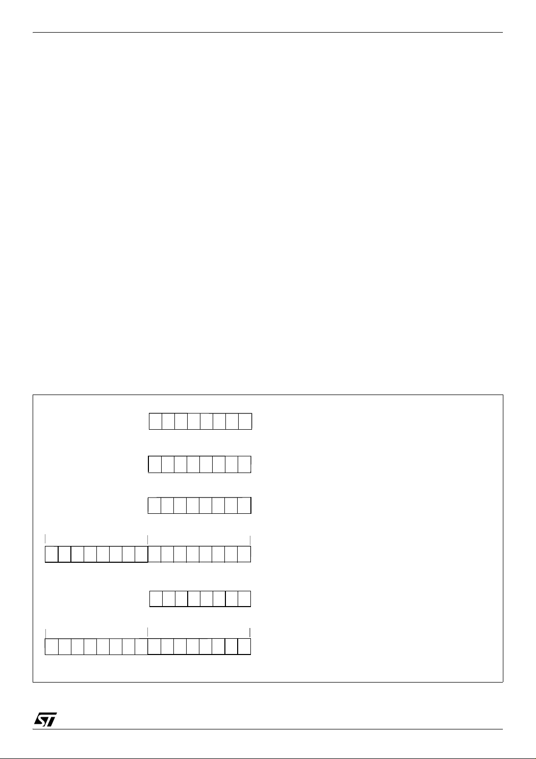
5 CENTRAL PROCESSING UNIT
5.1 INTRODUCTION
This CPU has a full 8-bit architecture and contains
six internal registers allowing efficient 8-bit data
manipulation.
5.2 MAIN FEATURES
■ Enable executing 63 basic instructions
■ Fast 8-bit by 8-bit multiply
■ 17 main addressing modes (with indirect
addressing mode)
■ Two 8-bit index registers
■ 16-bit stack pointer
■ Low power HALT and WAIT modes
■ Priority maskable hardware interrupts
■ Non-maskable software/hardware interrupts
5.3 CPU REGISTERS
The six CPU registers shown in Figure 1 are not
present in the memory mapping and are accessed
by specific instructions.
Accumulator (A)
The Accumulator is an 8-bit general purpose reg-
ister used to hold operands and the results of the
arithmetic and logic calculations and to manipulate
data.
Index Registers (X and Y)
These 8-bit registers are used to create effective
addresses or as temporary storage areas for data
manipulation. (The Cross-Assembler generates a
precede instruction (PRE) to indicate that the fol-
lowing instruction refers to the Y register.)
The Y register is not affected by the interrupt auto-
matic procedures.
Program Counter (PC)
The program counter is a 16-bit register containing
the address of the next instruction to be executed
by the CPU. It is made of two 8-bit registers PCL
(Program Counter Low which is the LSB) and PCH
(Program Counter High which is the MSB).
Figure 8. CPU Registers
ACCUMULATOR
X INDEX REGISTER
Y INDEX REGISTER
STACK POINTER
CONDITION CODE REGISTER
PROGRAM COUNTER
70
1C1I1HI0NZ
RESET VALUE = RESET VECTOR @ FFFEh-FFFFh
70
70
70
0
7
15 8
PCH
PCL
15
8
70
RESET VALUE = STACK HIGHER ADDRESS
RESET VALUE =
1X11X1XX
RESET VALUE = XXh
RESET VALUE = XXh
RESET VALUE = XXh
X = Undefined Value
ST72321Rx ST72321ARx ST72321Jx
22/193
CENTRAL PROCESSING UNIT (Cont’d)
Condition Code Register (CC)
Read/Write
Reset Value: 111x1xxx
The 8-bit Condition Code register contains the in-
terrupt masks and four flags representative of the
result of the instruction just executed. This register
can also be handled by the PUSH and POP in-
structions.
These bits can be individually tested and/or con-
trolled by specific instructions.
Arithmetic Management Bits
Bit 4 = H Half carry.
This bit is set by hardware when a carry occurs be-
tween bits 3 and 4 of the ALU during an ADD or
ADC instructions. It is reset by hardware during
the same instructions.
0: No half carry has occurred.
1: A half carry has occurred.
This bit is tested using the JRH or JRNH instruc-
tion. The H bit is useful in BCD arithmetic subrou-
tines.
Bit 2 = N Negative.
This bit is set and cleared by hardware. It is repre-
sentative of the result sign of the last arithmetic,
logical or data manipulation. It’s a copy of the re-
sult 7
th
bit.
0: The result of the last operation is positive or null.
1: The result of the last operation is negative
(that is, the most significant bit is a logic 1).
This bit is accessed by the JRMI and JRPL instruc-
tions.
Bit 1 = Z Zero.
This bit is set and cleared by hardware. This bit in-
dicates that the result of the last arithmetic, logical
or data manipulation is zero.
0: The result of the last operation is different from
zero.
1: The result of the last operation is zero.
This bit is accessed by the JREQ and JRNE test
instructions.
Bit 0 = C Carry/borrow.
This bit is set and cleared by hardware and soft-
ware. It indicates an overflow or an underflow has
occurred during the last arithmetic operation.
0: No overflow or underflow has occurred.
1: An overflow or underflow has occurred.
This bit is driven by the SCF and RCF instructions
and tested by the JRC and JRNC instructions. It is
also affected by the “bit test and branch”, shift and
rotate instructions.
Interrupt Management Bits
Bit 5,3 = I1, I0 Interrupt
The combination of the I1 and I0 bits gives the cur-
rent interrupt software priority.
These two bits are set/cleared by hardware when
entering in interrupt. The loaded value is given by
the corresponding bits in the interrupt software pri-
ority registers (IxSPR). They can be also set/
cleared by software with the RIM, SIM, IRET,
HALT, WFI and PUSH/POP instructions.
See the interrupt management chapter for more
details.
70
11I1HI0NZ
C
Interrupt Software Priority I1 I0
Level 0 (main) 1 0
Level 1 0 1
Level 2 0 0
Level 3 (= interrupt disable) 1 1
ST72321Rx ST72321ARx ST72321Jx
23/193
CENTRAL PROCESSING UNIT (Cont’d)
Stack Pointer (SP)
Read/Write
Reset Value: 01 FFh
The Stack Pointer is a 16-bit register which is al-
ways pointing to the next free location in the stack.
It is then decremented after data has been pushed
onto the stack and incremented before data is
popped from the stack (see Figure 2).
Since the stack is 256 bytes deep, the 8 most sig-
nificant bits are forced by hardware. Following an
MCU Reset, or after a Reset Stack Pointer instruc-
tion (RSP), the Stack Pointer contains its reset val-
ue (the SP7 to SP0 bits are set) which is the stack
higher address.
The least significant byte of the Stack Pointer
(called S) can be directly accessed by a LD in-
struction.
Note: When the lower limit is exceeded, the Stack
Pointer wraps around to the stack upper limit, with-
out indicating the stack overflow. The previously
stored information is then overwritten and there-
fore lost. The stack also wraps in case of an under-
flow.
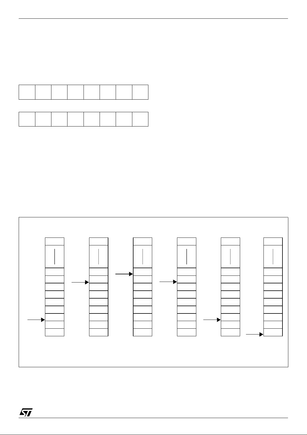
The stack is used to save the return address dur-
ing a subroutine call and the CPU context during
an interrupt. The user may also directly manipulate
the stack by means of the PUSH and POP instruc-
tions. In the case of an interrupt, the PCL is stored
at the first location pointed to by the SP. Then the
other registers are stored in the next locations as
shown in Figure 2.
– When an interrupt is received, the SP is decre-
mented and the context is pushed on the stack.
– On return from interrupt, the SP is incremented
and the context is popped from the stack.
A subroutine call occupies two locations and an in-
terrupt five locations in the stack area.
Figure 9. Stack Manipulation Example
15 8
00000001
70
SP7 SP6 SP5 SP4 SP3 SP2 SP1
SP0
PCH
PCL
SP
PCH
PCL
SP
PCL
PCH
X
A
CC
PCH
PCL
SP
PCL
PCH
X
A
CC
PCH
PCL
SP
PCL
PCH
X
A
CC
PCH
PCL
SP
SP
Y
CALL
Subroutine
Interrupt
Event
PUSH Y POP Y IRET
RET
or RSP
@ 01FFh
@ 0100h
Stack Higher Address = 01FFh
Stack Lower Address =
0100h
ST72321Rx ST72321ARx ST72321Jx
24/193
6 SUPPLY, RESET AND CLOCK MANAGEMENT
The device includes a range of utility features for
securing the application in critical situations (for
example in case of a power brown-out), and re-
ducing the number of external components. An
overview is shown in Figure 11.
For more details, refer to dedicated parametric
section.
Main features
■ Optional PLL for multiplying the frequency by 2
(not to be used with internal RC oscillator)
■ Reset Sequence Manager (RSM)
■ Multi-Oscillator Clock Management (MO)
– 5 Crystal/Ceramic resonator oscillators
– 1 Internal RC oscillator
■ System Integrity Management (SI)
– Main supply Low voltage detection (LVD)
– Auxiliary Voltage detector (AVD) with interrupt
capability for monitoring the main supply or
the EVD pin
6.1 PHASE LOCKED LOOP
If the clock frequency input to the PLL is in the
range 2 to 4 MHz, the PLL can be used to multiply
the frequency by two to obtain an f
OSC2
of 4 to 8
MHz. The PLL is enabled by option byte. If the PLL
is disabled, then f
OSC2 =
f
OSC
/2.
Caution: The PLL is not recommended for appli-
cations where timing accuracy is required. See
“PLL Characteristics” on page 151.
Figure 10. PLL Block Diagram
Figure 11. Clock, Reset and Supply Block Diagram
0
1
PLL OPTION BIT
PLL x 2
f
OSC2
/ 2
f
OSC
LOW VOLTAGE
DETECTOR
(LVD)
f
OSC2
AUXILIARY VOLTAGE
DETECTOR
(AVD)
MULTI-
OSCILLATOR
(MO)
OSC1
RESET
V
SS
EVD
V
DD
RESET SEQUENCE
MANAGER
(RSM)
OSC2
MAIN CLOCK
AVD Interrupt Request
CONTROLLER
PLL
SYSTEM INTEGRITY MANAGEMENT
WATCHDOG
SICSR
TIMER (WDG)
WITH REALTIME
CLOCK (MCC/RTC)
AVD
AVD AVD
LVD
RF
IE
WDG
RF
0
1
f
OSC
(option)
0
S
F
f
CPU
00
ST72321Rx ST72321ARx ST72321Jx
25/193
6.2 MULTI-OSCILLATOR (MO)
The main clock of the ST7 can be generated by
three different source types coming from the multi-
oscillator block:
■ an external source
■ 4 crystal or ceramic resonator oscillators
■ an internal high frequency RC oscillator
Each oscillator is optimized for a given frequency
range in terms of consumption and is selectable
through the option byte. The associated hardware
configurations are shown in Table 5. Refer to the
electrical characteristics section for more details.
Caution: The OSC1 and/or OSC2 pins must not
be left unconnected. For the purposes of Failure
Mode and Effect Analysis, it should be noted that if
the OSC1 and/or OSC2 pins are left unconnected,
the ST7 main oscillator may start and, in this con-
figuration, could generate an f
OSC
clock frequency
in excess of the allowed maximum (>16MHz.),
putting the ST7 in an unsafe/undefined state. The
product behaviour must therefore be considered
undefined when the OSC pins are left unconnect-
ed.
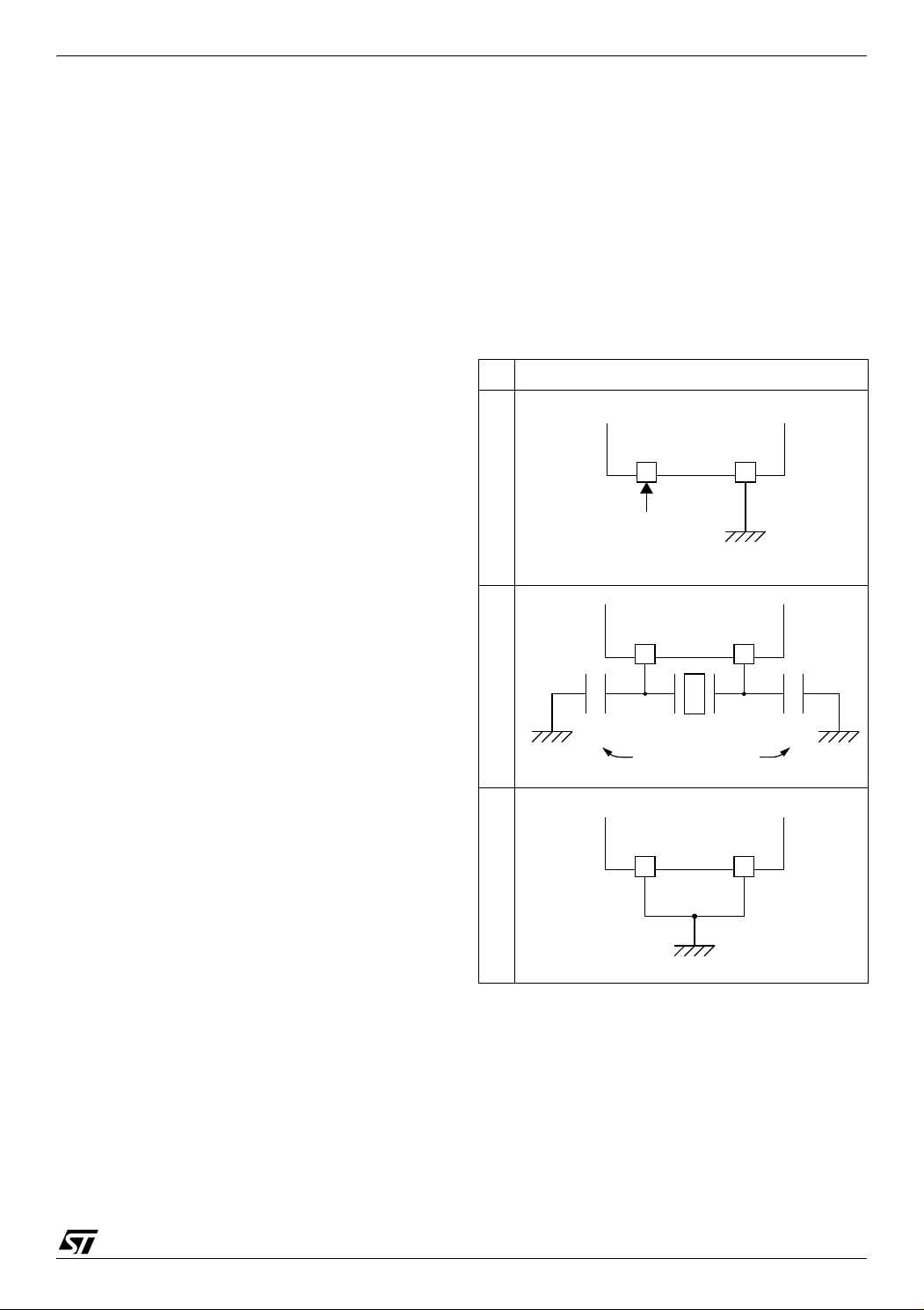
External Clock Source
In this external clock mode, a clock signal (square,
sinus or triangle) with ~50% duty cycle has to drive
the OSC1 pin while the OSC2 pin is tied to ground.
Crystal/Ceramic Oscillators
This family of oscillators has the advantage of pro-
ducing a very accurate rate on the main clock of
the ST7. The selection within a list of 4 oscillators
with different frequency ranges has to be done by
option byte in order to reduce consumption (refer
to section 14.1 on page 175 for more details on the
frequency ranges). In this mode of the multi-oscil-
lator, the resonator and the load capacitors have
to be placed as close as possible to the oscillator
pins in order to minimize output distortion and
start-up stabilization time. The loading capaci-
tance values must be adjusted according to the
selected oscillator.
These oscillators are not stopped during the
RESET phase to avoid losing time in the oscillator
start-up phase.
Internal RC Oscillator
This oscillator allows a low cost solution for the
main clock of the ST7 using only an internal resis-
tor and capacitor. Internal RC oscillator mode has
the drawback of a lower frequency accuracy and
should not be used in applications that require ac-
curate timing.
In this mode, the two oscillator pins have to be tied
to ground.
Table 5. ST7 Clock Sources
Hardware Configuration
External ClockCrystal/Ceramic ResonatorsInternal RC Oscillator
OSC1 OSC2
EXTERNAL
ST7
SOURCE
OSC1 OSC2
LOAD
CAPACITORS
ST7
C
L2
C
L1
OSC1 OSC2
ST7
ST72321Rx ST72321ARx ST72321Jx
26/193
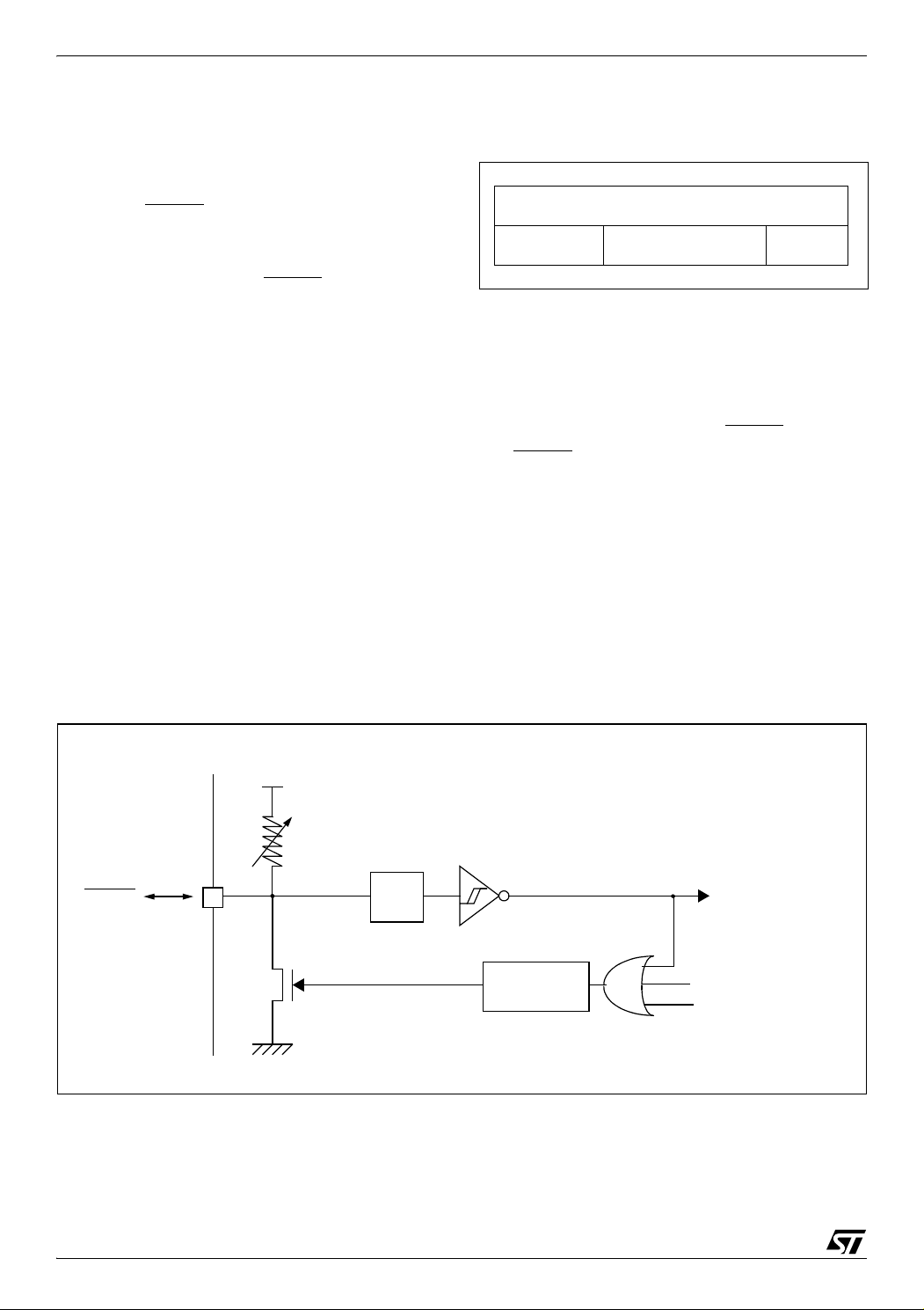
6.3 RESET SEQUENCE MANAGER (RSM)
6.3.1 Introduction
The reset sequence manager includes three RE-
SET sources as shown in Figure 13:
■ External RESET source pulse
■ Internal LVD RESET (Low Voltage Detection)
■ Internal WATCHDOG RESET
These sources act on the RESET
pin and it is al-
ways kept low during the delay phase.
The RESET service routine vector is fixed at ad-
dresses FFFEh-FFFFh in the ST7 memory map.
The basic RESET sequence consists of 3 phases
as shown in Figure 12:
■ Active Phase depending on the RESET source
■ 256 or 4096 CPU clock cycle delay (selected by
option byte)
■ RESET vector fetch
The 256 or 4096 CPU clock cycle delay allows the
oscillator to stabilise and ensures that recovery
has taken place from the Reset state. The shorter
or longer clock cycle delay should be selected by
option byte to correspond to the stabilization time
of the external oscillator used in the application
(see section 14.1 on page 175).
The RESET vector fetch phase duration is 2 clock
cycles.
Figure 12. RESET Sequence Phases
Caution: When the ST7 is unprogrammed or fully
erased, the Flash is blank and the RESET vector
is not programmed.
For this reason, it is recommended to keep the
RESET pin in low state until programming mode is
entered, in order to avoid unwanted behavior.
6.3.2 Asynchronous External RESET
pin
The RESET
pin is both an input and an open-drain
output with integrated R
ON
weak pull-up resistor.
This pull-up has no fixed value but varies in ac-
cordance with the input voltage. It
can be pulled
low by external circuitry to reset the device. See
“CONTROL PIN CHARACTERISTICS” on
page 159 for more details.
A RESET signal originating from an external
source must have a duration of at least t
h(RSTL)in
in
order to be recognized (see Figure 14). This de-
tection is asynchronous and therefore the MCU
can enter reset state even in HALT mode.
Figure 13. Reset Block Diagram
RESET
Active Phase
INTERNAL RESET
256 or 4096 CLOCK CYCLES
FETCH
VECTOR
RESET
R
ON
V
DD
WATCHDOG RESET
LVD RESET
INTERNAL
RESET
PULSE
GENERATOR
Filter
ST72321Rx ST72321ARx ST72321Jx
27/193
RESET SEQUENCE MANAGER (Cont’d)
The RESET
pin is an asynchronous signal which
plays a major role in EMS performance. In a noisy
environment, it is recommended to follow the
guidelines mentioned in the electrical characteris-
tics section.
If the external RESET
pulse is shorter than
t
w(RSTL)out
(see short ext. Reset in Figure 14), the
signal on the RESET
pin may be stretched. Other-
wise the delay will not be applied (see long ext.
Reset in Figure 14). Starting from the external RE-
SET pulse recognition, the device RESET
pin acts
as an output that is pulled low during at least
t
w(RSTL)out
.
6.3.3 External Power-On RESET
If the LVD is disabled by option byte, to start up the
microcontroller correctly, the user must ensure by
means of an external reset circuit that the reset
signal is held low until V
DD
is over the minimum
level specified for the selected f
OSC
frequency.
(see “OPERATING CONDITIONS” on page 140)
A proper reset signal for a slow rising V
DD
supply
can generally be provided by an external RC net-
work connected to the RESET
pin.
6.3.4 Internal Low Voltage Detector (LVD)
RESET
Two different RESET sequences caused by the in-
ternal LVD circuitry can be distinguished:
■ Power-On RESET
■ Voltage Drop RESET
The device RESET
pin acts as an output that is
pulled low when V
DD
<V
IT+
(rising edge) or
V
DD
<V
IT-
(falling edge) as shown in Figure 14.
The LVD filters spikes on V
DD
larger than t
g(VDD)
to
avoid parasitic resets.
6.3.5 Internal Watchdog RESET
The RESET sequence generated by a internal
Watchdog counter overflow is shown in Figure 14.
Starting from the Watchdog counter underflow, the
device RESET
pin acts as an output that is pulled
low during at least t
w(RSTL)out
.
Figure 14. RESET Sequences
V
DD
RUN
RESET PIN
EXTERNAL
WATCHDOG
ACTIVE PHASE
V
IT+(LVD)
V
IT-(LVD)
t
h(RSTL)in
t
w(RSTL)out
RUN
t
h(RSTL)in
ACTIVE
WATCHDOG UNDERFLOW
t
w(RSTL)out
RUN RUN RUN
RESET
RESET
SOURCE
SHORT EXT.
RESET
LVD
RESET
LONG EXT.
RESET
WATCHDOG
RESET
INTERNAL RESET (256 or 4096 T
CPU
)
VECTOR FETCH
t
w(RSTL)out
PHASE
ACTIVE
PHASE
ACTIVE
PHASE
DELAY
ST72321Rx ST72321ARx ST72321Jx
28/193
6.4 SYSTEM INTEGRITY MANAGEMENT (SI)
The System Integrity Management block contains
the Low Voltage Detector (LVD), Auxiliary Volt-
age Detector (AVD) functions. It is managed by
the SICSR register.
6.4.1 Low Voltage Detector (LVD)
The Low Voltage Detector function (LVD) gener-
ates a static reset when the V
DD
supply voltage is
below a V
IT-
reference value. This means that it
secures the power-up as well as the power-down
keeping the ST7 in reset.
The V
IT-
reference value for a voltage drop is lower
than the V
IT+
reference value for power-on in order
to avoid a parasitic reset when the MCU starts run-
ning and sinks current on the supply (hysteresis).
The LVD Reset circuitry generates a reset when
V
DD
is below:
–V
IT+
when V
DD
is rising
–V
IT-
when V
DD
is falling
The LVD function is illustrated in Figure 15.
The voltage threshold can be configured by option
byte to be low, medium or high.
Provided the minimum V
DD
value (guaranteed for
the oscillator frequency) is above V
IT-
, the MCU
can only be in two modes:
– under full software control
– in static safe reset
In these conditions, secure operation is always en-
sured for the application without the need for ex-
ternal reset hardware.
During a Low Voltage Detector Reset, the RESET
pin is held low, thus permitting the MCU to reset
other devices.
Notes:
The LVD allows the device to be used without any
external RESET circuitry.
If the medium or low thresholds are selected, the
detection may occur outside the specified operat-
ing voltage range. Below 3.8V, device operation is
not guaranteed.
The LVD is an optional function which can be se-
lected by option byte.
It is recommended to make sure that the V
DD
sup-
ply voltage rises monotonously when the device is
exiting from Reset, to ensure the application func-
tions properly.
Figure 15. Low Voltage Detector vs Reset
V
DD
V
IT+
RESET
V
IT-
V
hys
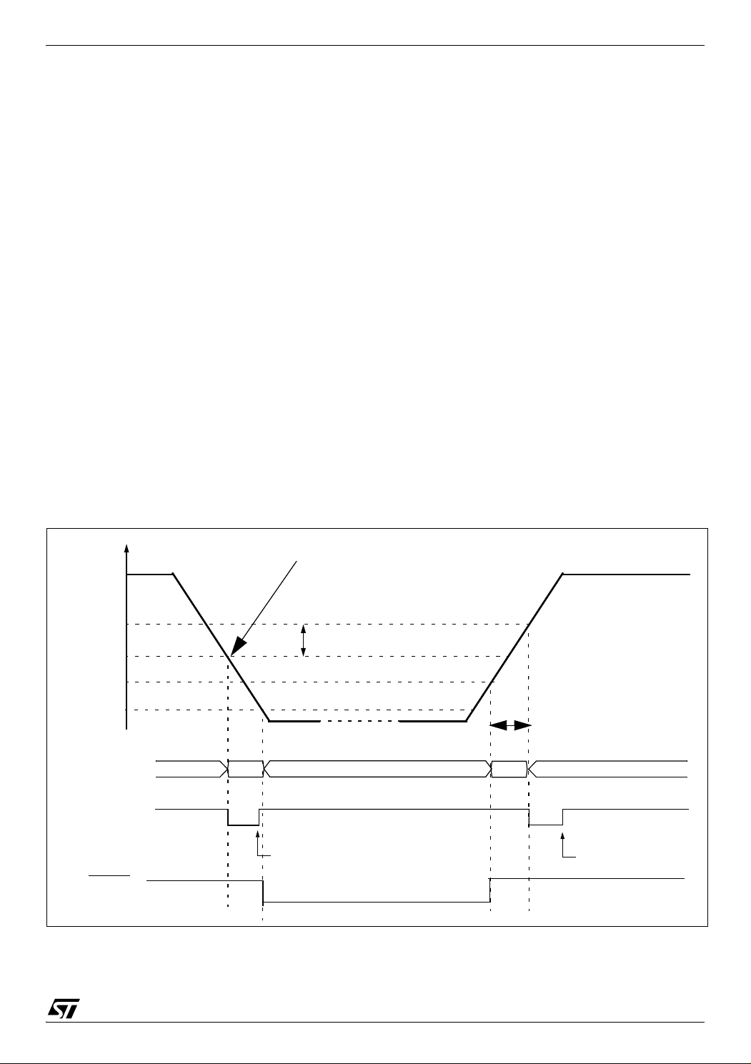
ST72321Rx ST72321ARx ST72321Jx
29/193
SYSTEM INTEGRITY MANAGEMENT (Cont’d)
6.4.2 Auxiliary Voltage Detector (AVD)
The Voltage Detector function (AVD) is based on
an analog comparison between a V
IT-(AVD)
and
V
IT+(AVD)
reference value and the V
DD
main sup-
ply or the external EVD pin voltage level (V
EVD
).
The V
IT-
reference value for falling voltage is lower
than the V
IT+
reference value for rising voltage in
order to avoid parasitic detection (hysteresis).
The output of the AVD comparator is directly read-
able by the application software through a real
time status bit (AVDF) in the SICSR register. This
bit is read only.
Caution: The AVD function is active only if the
LVD is enabled through the option byte.
6.4.2.1 Monitoring the V
DD
Main Supply
This mode is selected by clearing the AVDS bit in
the SICSR register.
The AVD voltage threshold value is relative to the
selected LVD threshold configured by option byte
(see section 14.1 on page 175).
If the AVD interrupt is enabled, an interrupt is gen-
erated when the voltage crosses the V
IT+(AVD)
or
V
IT-(AVD)
threshold (AVDF bit toggles).
In the case of a drop in voltage, the AVD interrupt
acts as an early warning, allowing software to shut
down safely before the LVD resets the microcon-
troller. See Figure 16.
The interrupt on the rising edge is used to inform
the application that the V
DD
warning state is over.
If the voltage rise time t
rv
is less than 256 or 4096
CPU cycles (depending on the reset delay select-
ed by option byte), no AVD interrupt will be gener-
ated when V
IT+(AVD)
is reached.
If t
rv
is greater than 256 or 4096 cycles then:
– If the AVD interrupt is enabled before the
V
IT+(AVD)
threshold is reached, then 2 AVD inter-
rupts will be received: the first when the AVDIE
bit is set, and the second when the threshold is
reached.
– If the AVD interrupt is enabled after the V
IT+(AVD)
threshold is reached then only one AVD interrupt
will occur.
Figure 16. Using the AVD to Monitor V
DD
(AVDS bit=0)
V
DD
V
IT+(AVD)
V
IT-(AVD)
AVDF bit 0 0RESET VALUE
IF AVDIE bit = 1
V
hyst
AVD INTERRUPT
REQUEST
INTERRUPT PROCESS
INTERRUPT PROCESS
V
IT+(LVD)
V
IT-(LVD)
LVD RESET
Early Warning Interrupt
(Power has dropped, MCU not
not yet in reset)
1
1
t
rv
VOLTAGE RISE TIME
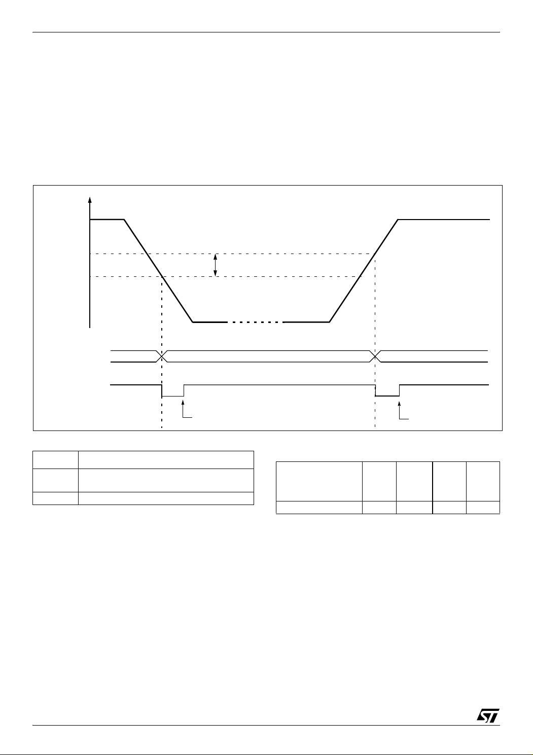
ST72321Rx ST72321ARx ST72321Jx
30/193
SYSTEM INTEGRITY MANAGEMENT (Cont’d)
6.4.2.2 Monitoring a Voltage on the EVD pin
This mode is selected by setting the AVDS bit in
the SICSR register.
The AVD circuitry can generate an interrupt when
the AVDIE bit of the SICSR register is set. This in-
terrupt is generated on the rising and falling edges
of the comparator output. This means it is generat-
ed when either one of these two events occur:
–V
EVD
rises up to V
IT+(EVD)
–V
EVD
falls down to V
IT-(EVD)
The EVD function is illustrated in Figure 17.
For more details, refer to the Electrical Character-
istics section.
Figure 17. Using the Voltage Detector to Monitor the EVD pin (AVDS bit=1)
6.4.3 Low Power Modes
6.4.3.1 Interrupts
The AVD interrupt event generate an interrupt if
the corresponding Enable Control Bit (AVDIE) is
set and the interrupt mask in the CC register is re-
set (RIM instruction).
V
EVD
V
IT+(EVD)
V
IT-(EVD)
AVDF 0 01
IF AVDIE = 1
V
hyst
AVD INTERRUPT
REQUEST
INTERRUPT PROCESS
INTERRUPT PROCESS
Mode Description
WAIT
No effect on SI. AVD interrupts cause the
device to exit from Wait mode.
HALT The SICSR register is frozen.
Interrupt Event
Event
Flag
Enable
Control
Bit
Exit
from
Wait
Exit
from
Halt
AVD event AVDF AVDIE Yes No
Loading...