


 Loading...
ST TSV521, TSV522, TSV524, TSV521A, TSV522A User Manual
...TSV521, TSV522, TSV524,
TSV521A, TSV522A, TSV524A
High merit factor (1.15 MHz for 45 µA) CMOS op amps
Features
■Gain bandwidth product: 1.15 MHz typ. at 5 V
■Low power consumption: 45 µA typ. at 5 V
■Rail-to-rail input and output
■Low input bias current: 1 pA typ.
■Supply voltage: 2.7 to 5.5 V
■Low offset voltage: 800 µV max.
■Unity gain stable on 100 pF capacitor
■Automotive grade
Benefits
■Increased lifetime in battery powered applications
■Easy interfacing with high impedance sensors
Related products
■See TSV6x series for lower minimum supply voltage (1.5 V)
■See LMV82x series for higher gain bandwidth products (5.5 MHz)
Applications
■Battery powered applications
■Portable devices
■Automotive signal conditioning
■Active filtering
■Medical instrumentation
Description
The TSV52x series of operational amplifiers offers low voltage operation and rail-to-rail input and output. The TSV521 device is the single version, the TSV522 device the dual version, and the TSV524 device the quad version, with pinouts compatible with industry standards.
Datasheet −preliminary data
SC70-5
DFN8 2 x 2 |
MiniSO8 |
QFN16 3 x 3 |
TSSOP14 |
The TSV52x series offers an outstanding speed/power consumption ratio, 1.15 MHz gain bandwidth product while consuming only 45 µA at 5 V. The devices are housed in the smallest industrial packages.
These features make the TSV52x family ideal for sensor interfaces, battery supplied and portable applications. The wide temperature range and high ESD tolerance facilitate their use in harsh automotive applications.
Table 1. |
Device summary |
|
|
|
|
Standard Vio |
Enhanced Vio |
Single |
|
TSV521 |
TSV521A |
|
|
|
|
Dual |
|
TSV522 |
TSV522A |
|
|
|
|
Quad |
|
TSV524 |
TSV524A |
|
|
|
|
June 2012 |
Doc ID 022743 Rev 1 |
1/27 |
This is preliminary information on a new product now in development or undergoing evaluation. Details are subject to |
www.st.com |
change without notice. |
|

Contents |
TSV521, TSV522, TSV524, TSV521A, TSV522A, TSV524A |
|
|
Contents
1 |
Package pin connections . . . . . . . . . . . . . . . . . . . . . . . . . . . . . . . . . . . . |
. 3 |
|
2 |
Absolute maximum ratings and operating conditions . . . . . . . . . . . . . |
4 |
|
3 |
Electrical characteristics . . . . . . . . . . . . . . . . . . . . . . . . . . . . . . . . . . . . . |
5 |
|
4 |
Application information . . . . . . . . . . . . . . . . . . . . . . . . . . . . . . . . . . . . . |
13 |
|
|
4.1 |
Operating voltages . . . . . . . . . . . . . . . . . . . . . . . . . . . . . . . . . . . . . . . . . . |
13 |
|
4.2 |
Common mode voltage range . . . . . . . . . . . . . . . . . . . . . . . . . . . . . . . . . |
13 |
|
4.3 |
Rail-to-rail input . . . . . . . . . . . . . . . . . . . . . . . . . . . . . . . . . . . . . . . . . . . . |
14 |
|
4.4 |
Rail-to-rail output . . . . . . . . . . . . . . . . . . . . . . . . . . . . . . . . . . . . . . . . . . . |
14 |
|
4.5 |
Driving resistive and capacitive loads . . . . . . . . . . . . . . . . . . . . . . . . . . . |
14 |
|
4.6 |
Input offset voltage drift over temperature . . . . . . . . . . . . . . . . . . . . . . . . |
15 |
|
4.7 |
Long term input offset voltage drift . . . . . . . . . . . . . . . . . . . . . . . . . . . . . . |
16 |
|
4.8 |
PCB layouts . . . . . . . . . . . . . . . . . . . . . . . . . . . . . . . . . . . . . . . . . . . . . . . |
17 |
|
4.9 |
Macromodel . . . . . . . . . . . . . . . . . . . . . . . . . . . . . . . . . . . . . . . . . . . . . . . |
17 |
5 |
Package information . . . . . . . . . . . . . . . . . . . . . . . . . . . . . . . . . . . . . . . . |
18 |
|
6 |
Ordering information . . . . . . . . . . . . . . . . . . . . . . . . . . . . . . . . . . . . . . . |
26 |
|
7 |
Revision history . . . . . . . . . . . . . . . . . . . . . . . . . . . . . . . . . . . . . . . . . . . |
26 |
|
2/27 |
Doc ID 022743 Rev 1 |

TSV521, TSV522, TSV524, TSV521A, TSV522A, TSV524A |
Package pin connections |
|
|
1 Package pin connections
Figure 1. Pin connections for each package (top view)
IN+ 1 |
5 |
VCC+ |
VCC- 2
IN- |
3 |
|
4 |
OUT |
|
|
|
|
|
TSV521 SC70-5
OUT1 |
1 |
|
8 |
VCC+ |
IN1- |
|
|
|
OUT2 |
2 |
7 |
|||
|
|
NC |
|
|
IN1+ |
3 |
6 |
IN2- |
|
VCC- |
4 |
5 |
IN2+ |
|
OUT1 1
IN1- 2
IN1+ 3
VCC- 4
8VCC+
7OUT2
6IN2-
5IN2+
|
|
|
|
|
TSV522 |
|
|
|
|
|
|
|
|
|
|
|
|
|
TSV522 |
|
|||||||||||||
|
|
|
|
|
DFN8 |
|
|
|
|
|
|
|
|
|
|
|
|
|
MiniSO8 |
|
|||||||||||||
|
|
|
IN1- |
|
OUT1 |
|
|
OUT4 |
IN4- |
|
|
|
|
|
|
|
|
|
|
|
|
|
|
|
|
|
|
|
|
|
|||
|
16 |
15 |
14 |
|
13 |
|
|
|
|
|
|
|
|
|
|
|
|
|
|
|
|
|
|
|
|
|
|
|
|||||
|
|
|
|
|
|
|
|
|
|
|
|
|
|
|
|
|
|
|
|
|
|
|
|
|
|||||||||
|
|
|
|
|
|
|
|
|
|
|
|
|
|
|
|
|
|
|
|
|
|
|
|
|
|
|
|
|
|
|
|
|
|
IN1+ |
|
|
|
|
|
|
|
|
|
|
|
|
IN4+ |
|
|
|
|
|
|
|
|
|
|
|
|
|
|
|
|
|
|
|
|
1 |
|
|
|
|
|
|
|
|
|
|
12 |
|
|
|
|
|
|
|
|
|
|
|
|
|
|
|
|||||||
|
|
|
|
|
|
|
|
|
|
|
|
|
|
|
|
|
|
|
|
|
|
|
|
|
|
|
|||||||
|
|
|
|
|
|
|
|
|
|
|
|
|
|
|
|
|
|
|
|
||||||||||||||
VCC+ |
2 |
|
|
|
|
NC |
11 |
VCC- |
|
|
|
|
|
|
|
|
|
|
|||||||||||||||
|
|
|
|
|
|
|
|
|
|||||||||||||||||||||||||
|
|
|
|
|
|
||||||||||||||||||||||||||||
|
|
|
|
|
|
|
|
|
|
|
|
|
|
|
|
|
|
|
|
|
|
|
|
|
|
|
|
|
|
||||
NC |
3 |
|
|
|
|
|
|
|
|
10 |
NC |
|
|
|
|
|
|||||||||||||||||
|
|
|
|
|
|
|
|
|
|
||||||||||||||||||||||||
|
|
|
|
|
|
|
|
|
|
|
|
|
|
|
|
|
|
|
|
|
|
|
|
|
|||||||||
IN2+ |
|
|
|
|
|
|
|
|
|
|
|
|
|
|
|
|
|
|
|
|
|
|
|
|
|
|
|
|
|
|
|
|
|
4 |
|
|
|
|
|
|
|
|
|
|
9 |
IN3+ |
|
|
|
|
|
||||||||||||||||
|
|
|
|
|
|
|
|
|
|
|
|
||||||||||||||||||||||
|
|
|
|
|
|
|
|
|
|
|
|
|
|
|
|
|
|
|
|
|
|
|
|
|
|
|
|||||||
|
|
|
|
|
|
|
|
|
|
|
|
|
|
|
|
|
|
|
|
|
|
|
|
|
|
|
|
|
|
|
|
|
|
|
|
|
|
|
|
|
|
|
|
|
|
|
|
|
|
|
|
|
|
|
|
|
|
|
|
|
|
|
|
|
|
|
|
|
|
5 |
|
6 |
|
|
7 |
|
8 |
|
|
|
|
|
|
|
|
|
|
|
|
|
|
|
|
|
|
|
|
|
|
|
|
|
|
|
|
|
|
|
|
|
|
|
|
|
|
|
|
|
|
|
|
|
|
|
|
|
|
|
|
|
|
|
|
|
|
|
|
|
IN2- |
|
OUT2 |
|
|
OUT3 |
IN3- |
|
|
|
|
|
|
|
|
|
|
|
|
|
|
|
|
|
|
|
|
|
|||
|
|
|
|
TSV524 |
|
|
|
|
|
|
|
|
|
|
|
|
|
TSV524 |
|
||||||||||||||
|
|
|
|
|
QFN16 |
|
|
|
|
|
|
|
|
|
|
|
|
|
TSSOP14 |
|
|||||||||||||
Doc ID 022743 Rev 1 |
3/27 |

Absolute maximum ratings and operating conditions |
TSV521, TSV522, TSV524, TSV521A, |
|
|
2 Absolute maximum ratings and operating conditions
Table 2. |
Absolute maximum ratings (AMR) |
|
|
|
|
|
Symbol |
Parameter |
|
|
Value |
Unit |
|
|
|
|
|
|
|
|
VCC |
Supply voltage(1) |
|
|
6 |
V |
|
Vid |
Differential input voltage(2) |
|
|
±VCC |
V |
|
V |
in |
Input voltage(3) |
V |
CC- |
- 0.2 to V + 0.2 |
V |
|
|
|
CC+ |
|
||
Iin |
Input current(4) |
|
|
10 |
mA |
|
Tstg |
Storage temperature |
|
|
-65 to +150 |
°C |
|
|
|
Thermal resistance junction-to-ambient(5),(6) |
|
|
|
|
|
|
SC70-5 |
|
|
205 |
|
Rthja |
DFN8 2 x 2 |
|
|
57 |
°C/W |
|
QFN16 3 x 3 |
|
|
45 |
|||
|
|
|
|
|
||
|
|
MiniSO8 |
|
|
190 |
|
|
|
TSSOP14 |
|
|
100 |
|
|
|
|
|
|
|
|
Tj |
Maximum junction temperature |
|
|
150 |
°C |
|
|
|
HBM: human body model(7) |
|
|
4 |
kV |
|
|
MM: machine model(8) |
|
|
300 |
V |
ESD |
|
|
|
|
|
|
CDM: charged device model(9) |
|
|
1.5 |
kV |
||
|
|
(all packages except SC70-5 and DFN8) |
|
|
||
|
|
|
|
|
|
|
|
|
|
|
|
|
|
|
|
CDM: charged device model (SC70-5 and DFN8)(9) |
|
|
1.3 |
kV |
|
|
Latch-up immunity |
|
|
200 |
mA |
|
|
|
|
|
|
|
1.All voltage values, except differential voltages are with respect to network ground terminal.
2.Differential voltages are the non inverting input terminal with respect to the inverting input terminal.
3.VCC - Vin must not exceed 6 V, Vin must not exceed 6 V.
4.Input current must be limited by a resistor in series with the inputs.
5.Short-circuits can cause excessive heating and destructive dissipation.
6.Rth are typical values.
7.Human body model: 100 pF discharged through a 1.5 kΩ resistor between two pins of the device, done for all couples of pin combinations with other pins floating.
8.Machine model: a 200 pF cap is charged to the specified voltage, then discharged directly between two pins of the device with no external series resistor (internal resistor < 5 Ω), done for all couples of pin combinations with other pins floating.
9.Charged device model: all pins plus package are charged together to the specified voltage and then discharged directly to ground.
Table 3. |
Operating conditions |
|
|
Symbol |
Parameter |
Value |
Unit |
|
|
|
|
VCC |
Supply voltage |
2.7 to 5.5 |
V |
Vicm |
Common mode input voltage range |
VCC- - 0.1 to VCC+ + 0.1 |
V |
Toper |
Operating free air temperature range |
-40 to +125 |
°C |
4/27 |
Doc ID 022743 Rev 1 |

TSV521, TSV522, TSV524, TSV521A, TSV522A, TSV524A Electrical characteristics
3 |
Electrical characteristics |
|
|
|
|
|
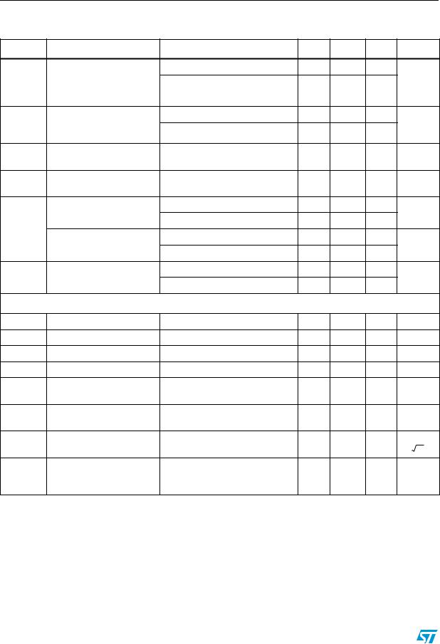
Table 4. |
Electrical characteristics at VCC+ = +2.7 V with VCC- = 0 V, Vicm = VCC/2, T = 25 °C, and |
|||||
|
RL = 10 kΩ connected to VCC/2 (unless otherwise specified) |
|
|
|
||
Symbol |
Parameter |
Conditions |
Min. |
Typ. |
Max. |
Unit |
|
|
|
|
|
|
|
DC performance |
|
|
|
|
|
|
|
|
|
|
|
|
|
|
|
TSV52xA, T = 25 °C |
|
|
800 |
µV |
|
|
|
|
|
|
|
Vio |
Offset voltage |
TSV52xA, -40 °C < T < 125 °C |
|
|
2600 |
µV |
|
|
|
|
|
||
TSV52x, T = 25 °C |
|
|
1.5 |
mV |
||
|
|
|
|
|||
|
|
|
|
|
|
|
|
|
TSV52x, -40 °C < T < 125 °C |
|
|
3.3 |
mV |
|
|
|
|
|
|
|
Vio/ T |
Input offset voltage drift |
-40 °C < T < 125 °C(1) |
|
3 |
18 |
µV/°C |
Iio |
Input offset current |
T = 25 °C |
|
1 |
10(3) |
pA |
|
|
|
|
|
||
(Vout = VCC/2) |
-40° C < T < 125 °C |
|
1 |
100(3) |
pA |
|
|
|
|||||
Iib |
Input bias current |
T = 25 °C |
|
1 |
10(3) |
pA |
|
|
|
|
|
||
(Vout = VCC/2) |
-40 °C < T < 125 °C |
|
1 |
100(3) |
pA |
|
|
|
|||||
|
Common mode rejection |
T = 25 °C |
50 |
72 |
|
|
CMR |
ratio 20 log ( Vic/ Vio) |
|
|
|
|
dB |
|
|
|
|
|||
|
Vic = -0.1 V to VCC+0.1V, |
-40 °C < T < 125 °C |
46 |
|
|
|
|
Vout = VCC/2, RL = 1 MΩ |
|
|
|
|
|
|
Large signal voltage gain |
T = 25 °C |
90 |
105 |
|
|
Avd |
Vout = 0.5 V to (VCC - 0.5V), |
|
|
|
|
dB |
-40 °C < T < 125 °C |
60 |
|
|
|||
|
RL = 1 MΩ |
|
|
|
||
VOH |
High level output voltage |
T = 25 °C |
|
3 |
35 |
mV |
-40 °C < T < 125 °C |
|
|
50 |
|||
VOL |
Low level output voltage |
T = 25 °C |
|
6 |
35 |
mV |
-40 °C < T < 125 °C |
|
|
50 |
|||
|
Isink |
Vout = VCC, T = 25 °C |
12 |
22 |
|
mA |
Iout |
Vout = VCC, -40 °C < T < 125 °C |
8 |
|
|
||
|
|
|
|
|||
Isource |
Vout = 0 V, T = 25 °C |
12 |
18 |
|
mA |
|
|
|
|||||
|
Vout = 0 V, -40 °C < T < 125 °C |
8 |
|
|
||
|
|
|
|
|
||
ICC |
Supply current (per channel) |
T = 25 °C |
|
30 |
51 |
µA |
Vout = VCC/2, RL > 1 MΩ |
-40 °C < T < 125 °C |
|
30 |
51 |
||
|
|
|
||||
|
|
|
|
|
|
|
AC performance |
|
|
|
|
|
|
|
|
|
|
|
|
|
GBP |
Gain bandwidth product |
RL = 10 kΩ, CL = 100 pF |
0.62 |
1 |
|
MHz |
Fu |
Unity gain frequency |
RL = 10 kΩ, CL = 100 pF |
|
900 |
|
kHz |
Φm |
Phase margin |
RL = 10 kΩ, CL = 100 pF |
|
55 |
|
degrees |
Gm |
Gain margin |
RL = 10 kΩ, CL = 100 pF |
|
7 |
|
dB |
SR |
Slew rate |
RL = 10 kΩ, CL = 100 pF, |
|
0.74 |
|
V/µs |
|
|
Vout = 0.5 V to VCC - 0.5 V |
|
|
|
|
Doc ID 022743 Rev 1 |
5/27 |

Electrical characteristics |
TSV521, TSV522, TSV524, TSV521A, TSV522A, TSV524A |
||||||||
|
|
|
|
|
|
|
|||
Table 4. |
Electrical characteristics at VCC+ = +2.7 V with VCC- = 0 V, Vicm = VCC/2, T = 25 °C, and |
||||||||
|
|
|
RL = 10 kΩ connected to VCC/2 (unless otherwise specified) (continued) |
|
|||||
Symbol |
Parameter |
|
Conditions |
Min. |
Typ. |
Max. |
Unit |
||
|
|
|
|
|
|
|
|
|
|
|
|
|
Equivalent input noise |
f = 1 kHz |
|
|
61 |
|
nV |
en |
voltage |
f = 10 kHz |
|
43 |
|
----------- |
|||
|
|
Hz |
|||||||
|
|
|
Total harmonic distortion + |
Follower configuration, fin = 1 kHz, |
|
|
|
|
|
THD+N |
noise |
RL = 100 kΩ, Vicm = VCC/2, |
|
0.003 |
|
% |
|||
|
|
|
|
BW = 22 kHz, Vout = 1 Vpp |
|
|
|
|
|
Table 5. |
Electrical characteristics at VCC+ = +3.3 V with VCC- = 0 V, Vicm = VCC/2, T = 25 °C, and |
||||||||
|
|
|
RL = 10 kΩ connected to VCC/2 (unless otherwise specified) |
|
|
|
|||
Symbol |
Parameter |
|
Conditions |
Min. |
Typ. |
Max. |
Unit |
||
|
|
|
|
|
|
|
|
||
DC performance |
|
|
|
|
|
|
|||
|
|
|
|
|
|
|
|
|
|
|
|
|
|
TSV52xA, T = 25 °C |
|
|
600 |
µV |
|
|
|
|
|
|
|
|
|
|
|
Vio |
Offset voltage |
TSV52xA, -40 °C < T < 125 °C |
|
|
2400 |
µV |
|||
|
|
|
|
|
|
||||
TSV52x, T = 25 °C |
|
|
1.3 |
mV |
|||||
|
|
|
|
|
|
||||
|
|
|
|
|
|
|
|
|
|
|
|
|
|
TSV52x, -40 °C < T < 125 °C |
|
|
3.1 |
mV |
|
|
|
|
|
|
|
|
|
|
|
V |
io |
/ T |
Input offset voltage drift |
-40 °C < T < 125 °C(1) |
|
3 |
18 |
µV/°C |
|
|
|
|
|
|
|
|
|
|
|
|
|
|
|
|
|
|
|
|
|
|
|
|
Long term input offset |
|
(2) |
|
|
|
μV |
|
Vio |
voltage drift |
T = 25 °C |
|
0.3 |
|
-------------------------- |
||
|
|
|
|
month |
|||||
|
Iio |
Input offset current |
T = 25 °C |
|
|
1 |
10(3) |
pA |
|
|
|
|
|
|
|
|
|||
|
(Vout = VCC/2) |
-40 °C < T < 125 °C |
|
1 |
100(3) |
pA |
|||
|
|
|
|
||||||
|
Iib |
Input bias current |
T = 25 °C |
|
|
1 |
10(3) |
pA |
|
|
|
|
|
|
|
|
|||
|
(Vout = VCC/2) |
-40 °C < T < 125 °C |
|
1 |
100(3) |
pA |
|||
|
|
|
|
||||||
|
|
|
Common mode rejection |
T = 25 °C |
|
51 |
73 |
|
|
CMR |
ratio 20 log ( Vic/ Vio) |
|
|
|
|
|
dB |
||
|
|
|
|
|
|||||
|
|
|
Vic = -0.1 V to VCC +0.1 V, |
-40 °C < T < 125 °C |
47 |
|
|
|
|
|
|
|
Vout = VCC/2, RL = 1 MΩ |
|
|
|
|
|
|
|
|
|
Large signal voltage gain |
T = 25 °C |
|
91 |
106 |
|
|
Avd |
Vout = 0.5 V to (VCC - 0.5 V), |
|
|
|
|
|
dB |
||
-40 °C < T < 125 °C |
63 |
|
|
||||||
|
|
|
RL = 1 MΩ |
|
|
|
|||
VOH |
High level output voltage |
T = 25 °C |
|
|
3 |
35 |
mV |
||
-40 °C < T < 125 °C |
|
|
50 |
||||||
VOL |
Low level output voltage |
T = 25 °C |
|
|
7 |
35 |
mV |
||
-40 °C < T < 125 °C |
|
|
50 |
||||||
|
|
|
Isink |
Vout = VCC, T = 25 °C |
20 |
31 |
|
mA |
|
Iout |
Vout = VCC, -40 °C < T < 125 °C |
17 |
|
|
|||||
|
|
|
|
||||||
Isource |
Vout = 0 V, T = 25 °C |
19 |
27 |
|
mA |
||||
|
|
|
|
||||||
|
|
|
Vout = 0 V, -40 °C < T < 125 °C |
17 |
|
|
|||
|
|
|
|
|
|
|
|||
ICC |
Supply current (per channel) |
T = 25 °C |
|
|
32 |
55 |
µA |
||
Vout = VCC/2, RL > 1 MΩ |
-40 °C < T < 125 °C |
|
32 |
55 |
|||||
|
|
|
|
|
|||||
|
|
|
|
|
|
|
|
|
|
6/27 |
|
|
|
Doc ID 022743 Rev 1 |
|
|
|
|
|
|
|
|
|
|
|
|
|
|
|

TSV521, TSV522, TSV524, TSV521A, TSV522A, TSV524A |
|
|
Electrical characteristics |
|||||||||||
|
|
|
|
|
|
|
|
|
|
|
|
|
||
Table 5. |
|
Electrical characteristics at VCC+ = +3.3 V with VCC- = 0 V, Vicm = VCC/2, T = 25 °C, and |
||||||||||||
|
|
RL = 10 kΩ connected to VCC/2 (unless otherwise specified) (continued) |
|
|
||||||||||
Symbol |
|
Parameter |
|
|
Conditions |
|
Min. |
|
|
Typ. |
|
Max. |
|
Unit |
|
|
|
|
|
|
|
|
|
|
|
|
|
|
|
AC performance |
|
|
|
|
|
|
|
|
|
|
|
|
||
|
|
|
|
|
|
|
|
|
|
|
|
|
|
|
GBP |
Gain bandwidth product |
RL = 10 kΩ, CL = 100 pF |
0.64 |
|
1 |
|
|
|
MHz |
|||||
Fu |
Unity gain frequency |
RL = 10 kΩ, CL = 100 pF |
|
|
|
900 |
|
|
|
kHz |
||||
Φm |
Phase margin |
RL = 10 kΩ, CL = 100 pF |
|
|
|
55 |
|
|
|
degrees |
||||
Gm |
Gain margin |
RL = 10 kΩ, CL = 100 pF |
|
|
|
7 |
|
|
|
dB |
||||
SR |
Slew rate |
RL = 10 kΩ, CL = 100 pF, |
|
|
|
0.75 |
|
|
|
V/μs |
||||
|
|
|
Vout = 0.5 V to VCC - 0.5 V |
|
|
|
|
|
|
|
|
|
||
|
Equivalent input noise |
f = 1 kHz |
|
|
|
|
60 |
|
|
|
nV |
|||
en |
voltage |
f = 10 kHz |
|
|
|
|
42 |
|
|
----------- |
||||
|
|
|
|
|
|
|
Hz |
|||||||
|
Total harmonic distortion + |
Follower configuration, fin = 1 kHz, |
|
|
|
|
|
|
|
|
|
|||
THD+N |
noise |
RL = 100 kΩ, Vicm = VCC/2, |
|
|
|
0.003 |
|
|
% |
|||||
|
|
|
BW = 22 kHz, Vout = 1 Vpp |
|
|
|
|
|
|
|
|
|
||
Table 6. |
|
Electrical characteristics at VCC+ = +5 V with VCC- = 0 V, Vicm = VCC/2, T = 25 °C, |
||||||||||||
|
|
and RL = 10 kΩ connected to VCC/2 (unless otherwise specified) |
|
|
|
|
||||||||
Symbol |
|
Parameter |
|
|
Conditions |
|
Min. |
|
|
Typ. |
|
Max. |
|
Unit |
|
|
|
|
|
|
|
|
|
|
|
|
|
|
|
DC performance |
|
|
|
|
|
|
|
|
|
|
|
|
||
|
|
|
|
|
|
|
|
|
|
|
|
|
|
|
|
|
|
|
TSV52xA, T = 25 °C |
|
|
|
|
|
|
600 |
|
µV |
|
|
|
|
|
|
|
|
|
|
|
|
|
|
|
|
Vio |
|
Offset voltage |
|
TSV52xA, -40 °C < T < 125 °C |
|
|
|
|
|
|
2400 |
|
µV |
|
|
|
|
|
|
|
|
|
|
|
|
|
|
||
|
|
TSV52x, T = 25 °C |
|
|
|
|
|
|
1 |
|
mV |
|||
|
|
|
|
|
|
|
|
|
|
|
||||
|
|
|
|
|
|
|
|
|
|
|
|
|
|
|
|
|
|
|
TSV52x, -40 °C < T < 125 °C |
|
|
|
|
|
|
2.8 |
|
mV |
|
|
|
|
|
|
|
|
|
|
|
|
|
|
||
V / T |
|
Input offset voltage drift |
|
-40 °C < T < 125 °C(1) |
|
|
|
|
3 |
|
18 |
|
µV/°C |
|
io |
|
|
|
|
|
|
|
|
|
|
|
|
|
|
|
|
Long term input offset |
|
|
(2) |
|
|
|
|
|
|
|
|
μV |
Vio |
|
voltage drift |
|
T = 25 °C |
|
|
|
|
0.7 |
|
|
|
-------------------------- |
|
|
|
|
|
|
|
|
|
|
month |
|||||
Iio |
|
Input offset current |
|
T = 25 °C |
|
|
|
|
|
1 |
|
10(3) |
|
pA |
|
|
|
|
|
|
|
|
|
|
|
|
|
||
|
(Vout = VCC/2) |
|
-40 °C < T < 125 °C |
|
|
|
|
1 |
|
100(3) |
|
pA |
||
|
|
|
|
|
|
|
|
|||||||
Iib |
|
Input bias current |
|
T = 25 °C |
|
|
|
|
|
1 |
|
10(3) |
|
pA |
|
|
|
|
|
|
|
|
|
|
|
|
|
||
|
(Vout = VCC/2) |
|
-40 °C < T < 125 °C |
|
|
|
|
1 |
|
100(3) |
|
pA |
||
|
|
|
|
|
|
|
|
|||||||
|
|
Common mode rejection |
|
T = 25 °C |
|
|
54 |
|
|
76 |
|
|
|
|
CMR1 |
|
ratio 20 log ( Vic/ Vio) |
|
|
|
|
|
|
|
|
|
|
|
dB |
|
|
|
|
|
|
|
|
|
|
|
|
|||
|
|
Vic = -0.1 V to VCC +0.1 V, |
|
-40 °C < T < 125 °C |
|
50 |
|
|
|
|
|
|
|
|
|
|
Vout = VCC/2, RL = 1 MΩ |
|
|
|
|
|
|
|
|
|
|
|
|
|
|
Common mode rejection |
|
T = 25 °C |
|
|
63 |
|
|
84 |
|
|
|
|
CMR2 |
|
ratio 20 log ( Vic/ Vio) |
|
|
|
|
|
|
|
|
|
|
|
dB |
|
|
|
|
|
|
|
|
|
|
|
|
|||
|
|
Vic = 1 V to VCC -1 V, |
|
-40 °C < T < 125 °C |
|
58 |
|
|
|
|
|
|
|
|
|
|
Vout = VCC/2, RL = 1 MΩ |
|
|
|
|
|
|
|
|
|
|
|
|
Doc ID 022743 Rev 1 |
7/27 |
Electrical characteristics |
TSV521, TSV522, TSV524, TSV521A, TSV522A, TSV524A |
|||||
Table 6. |
Electrical characteristics at VCC+ = +5 V with VCC- = 0 V, Vicm = VCC/2, T = 25 °C, |
|||||
|
and RL = 10 kΩ connected to VCC/2 (unless otherwise specified) |
|
|
|||
Symbol |
Parameter |
Conditions |
Min. |
Typ. |
Max. |
Unit |
|
Supply voltage rejection |
T = 25 °C |
65 |
87 |
|
|
SVR |
ratio 20 log ( VCC/ Vio) |
|
|
|
|
dB |
|
VCC = 2.7 V to 5.5 V, |
-40 °C < T < 125 °C |
60 |
|
|
|
|
Vout = VCC/2 |
|
|
|
|
|
|
Large signal voltage gain |
T = 25 °C |
94 |
109 |
|
|
Avd |
Vout = 0.5 V to (VCC - 0.5 V), |
-40 °C < T < 125 °C |
68 |
|
|
dB |
|
RL = 1 MΩ |
|
|
|
||
VOH |
High level output voltage |
T = 25 °C |
|
5 |
35 |
mV |
-40 °C < T < 125 °C |
|
|
50 |
|||
VOL |
Low level output voltage |
T = 25 °C |
|
9 |
35 |
mV |
-40 °C < T < 125 °C |
|
|
50 |
|||
|
Isink |
Vout = VCC, T = 25 °C |
36 |
55 |
|
mA |
|
Vout = VCC, -40 °C < T < 125 °C |
27 |
|
|
||
Iout |
|
|
|
|
||
|
Vout = 0 V, T = 25 °C |
36 |
55 |
|
|
|
|
Isource |
|
mA |
|||
|
Vout = 0 V, -40 °C < T < 125 °C |
27 |
|
|
||
|
|
|
|
|
||
ICC |
Supply current (per channel) |
T = 25 °C |
|
45 |
60 |
µA |
Vout = VCC/2, RL > 1 MΩ |
-40 °C < T < 125 °C |
|
45 |
60 |
||
|
|
|
||||
AC performance |
|
|
|
|
|
|
GBP |
Gain bandwidth product |
RL = 10 kΩ, CL = 100 pF |
0.73 |
1.15 |
|
MHz |
Fu |
Unity gain frequency |
RL = 10 kΩ, CL = 100 pF |
|
900 |
|
kHz |
Φm |
Phase margin |
RL = 10 kΩ, CL = 100 pF |
|
55 |
|
degrees |
Gm |
Gain margin |
RL = 10 kΩ, CL = 100 pF |
|
7 |
|
dB |
SR |
Slew rate |
RL = 10 kΩ, CL = 100 pF, |
|
0.89 |
|
V/μs |
|
|
Vout = 0.5 V to VCC - 0.5V |
|
|
|
|
∫ en |
Low-frequency peak-to- |
Bandwidth: f = 0.1 to 10 Hz |
|
14 |
|
µVpp |
peak input noise |
|
|
||||
|
|
|
|
|
|
|
|
Equivalent input noise |
f = 1 kHz |
|
57 |
|
nV |
en |
voltage |
f = 10 kHz |
|
39 |
|
----------- |
|
|
Hz |
||||
|
Total harmonic distortion + |
Follower configuration, fin = 1 kHz, |
|
|
|
|
THD+N |
noise |
RL = 100 kΩ, Vicm = VCC/2, |
|
0.002 |
|
% |
|
|
BW = 22 kHz, Vout = 1 Vpp |
|
|
|
|
1.See Section 4.6: Input offset voltage drift over temperature on page 15.
2.Typical value is based on the Vio drift observed after 1000 h at 125 °C extrapolated to 25 °C using the Arrhenius law and assuming an activation energy of 0.7 eV. The operational amplifier is aged in follower mode configuration.
3.Guaranteed by design.
8/27 |
Doc ID 022743 Rev 1 |

TSV521, TSV522, TSV524, TSV521A, TSV522A, TSV524A |
Electrical characteristics |
|
|
Figure 2. Supply current vs. supply voltage Figure 3. at Vicm = VCC/2
Input offset voltage distribution at VCC = 5 V, Vicm = 2.5 V
|
|
|
|
|
|
|
|
|
|
|
6IO DISTRIBUTIONIAT 44 |
##FOR 6## 6 6ICM 6 |
|||||||
|
|
|
|
|
|
|
|
|
|
0OPULATIONA |
|
|
|
|
|
|
|
|
|
|
|
|
|
|
|
|
|
|
|
|
|
|
|
|
|
|
|
|
|
|
|
|
|
|
|
|
|
|
|
|
|
|
|
|
|
|
|
|
|
|
|
|
|
|
|
|
|
!- |
|
Figure 4. Input offset voltage temperature |
Figure 5. Input offset voltage vs. input |
coefficient distribution |
common mode voltage at VCC = 5 V |
|
|
|
|
|
|
|
|
|
|
|
|
|
|
|
|
|
|
|
|
|
|
|
6ICM 6## |
|
|
|
|
|
|
|
|
|
|
|
|
|
|
|
|
|
|
|
|
|
|
|
|
|
|
|
|
|
|
|
|
|
|
|
|
|
|
|
|
|
|
|
|
|
6## 6 |
|
|
|
|
|
|
|
|
|
|
|
|
|
|
|
|
|
|
|
|
|
|
|
|
|
|
|
|
|
|
|
|
|
|
|
|
|
|
|
|
|
|
|
|
|
0OPULATIONA |
|
|
|
|
|
|
|
|
|
|
|
|
|
|
|
44 # |
|
|
|
|
|
|
|
|
|
|
|
|
|
|
|
|
|
|
|
|
|
44 # |
|
|
|
|
|
||
|
|
|
|
|
|
|
|
|
|
|
|
|
|
|
|
|
|
|
|
|
|
|
|
|
|
|
|
|
|
|
|
|
|
|
|
|
|
|
|
|
|
|
|
44 # |
|
|
|
|
|
|
|
|
|
|
|
|
|
|
|
|
|
|
|
|
|
|
|
|
|
|
|
|
|
|
|
|
|
|
|
|
|
|
|
|
|
|
|
|
|
|
|
|
|
|
|
|
|
|
|
|
|
|
|
|
|
|
|
|
|
|
|
|
|
|
|
|
|
|
|
|
|
|
|
|
|
|
|
|
|
|
|
|
|
|
|
|
|
|
|
|
|
|
|
|
|
|
|
|
|
|
|
|
|
|
|
|
|
6## 6 |
||
|
|
|
|
|
|
|
|
|
|
|
|
|
|
|
|
|
|
|
|
|
|
|
|
|
|
|
|
|
|
|
|
||||||||||||||
|
|
|
|
|
|
|
|
|
|
|
|
|
!- |
|
|
|
|
6ICM 6 |
|
|
|
|
|
|
|
|
|
|
|
|
|
|
|
|
|
|
|
|
|
|
|
|
|
!- |
|
|
|
|
|
|
|
|
|
|
|
|
|
|
|
|
|
|
|
|
|
|
|
|
Figure 6. Input offset voltage vs. temperature Figure 7. Output current vs. output voltage at
|
at VCC = 5 V |
|
|
|
|
|
|
VCC = 2.7 V |
|
|
|
||
|
|
|
|
|
|
|
|
|
|
|
44 |
# |
|
|
|
|
,IMITMFOR 436 X! |
|
|
|
|
||||||
|
|
|
|
|
|
44 # |
|
||||||
|
|
|
|
|
|
|
|
||||||
|
|
|
|
|
|
|
|
|
|
|
|
||
|
|
,IMITMFOR 436 8 |
|
|
|
|
|
|
|
|
|
||
|
|
|
|
M! |
|
|
|
|
|
||||
|
|
|
|
|
|
|
|
|
|
|
44 |
# |
|
|
|
|
|
|
|
|
|
|
|
|
|||
|
|
|
|
|
|
|
CURRENT |
|
|
|
|
||
|
|
|
|
|
|
|
|
|
|
|
|
|
|
|
|
|
|
|
|
|
|
|
|
|
|
|
|
|
|
|
|
|
|
|
|
|
|
|
|
|
|
|
|
|
|
|
|
|
|
/UTPUT |
|
44 # 44 |
|
|
|
|
|
|
|
|
|
|
|
|
# |
|
|
||
|
|
|
|
|
|
|
|
|
|
|
|
|
|
|
|
|
|
|
|
|
|
|
|
|
|
|
|
|
|
6## 6 6ICM 6 |
|
|
|
|
|
|
|
||||
|
|
|
|
|
44 # |
|
6## 6 |
||||||
|
|
|
|
|
|
|
|
|
|
|
|||
|
|
|
|
|
|
|
|
|
|
|
|
||
|
|
|
|
|
|
|
|
|
|
|
|||
|
|
|
|
|
|
|
|
!- |
|
/UTPUT VOLTAGE 6 |
!- |
||
|
|
|
|
|
|
|
|
|
|
|
|
||
Doc ID 022743 Rev 1 |
9/27 |
Loading...