


 Loading...
ST LD39015XG08R, LD39015M08R, LD39015XG10R, LD39015M25R, LD39015M10R User Manual
...LD39015xx
150 mA low quiescent current low noise voltage regulator
Features
■Input voltage from 1.5 to 5.5 V
■Ultra low dropout voltage (80 mV typ. at 100 mA load)
■Very low quiescent current (18 µA typ. at no load, 35 µA typ. at 150 mA load, 1 µA max in off mode)
■Very low noise without bypass capacitor (29 µVRMS at VOUT = 0.8 V)
■Output voltage tolerance: ± 2.0% @ 25 °C
■150 mA guaranteed output current
■Wide range of output voltages available on request: 0.8 V to 3.3 V with 100 mV step
■Logic-controlled electronic shutdown
■Compatible with ceramic capacitors CO = 1 µF
■Internal current and thermal limit
■Available in SOT666 and SOT23-5L packages
■Temperature range: -40 °C to 125 °C
Description
The LD39015xx series provides 150 mA maximum current from an input voltage ranging
SOT666 |
SOT23-5L |
from 1.5 V to 5.5 V with a typical dropout voltage of 80 mV. It is stable with ceramic capacitor. The ultra-low drop voltage, low quiescent current and low noise features make it suitable for low power battery-powered applications. Power supply rejection is 65 dB at low frequencies and starts to roll off at 10 kHz. Enable logic control function puts the LD39015xx in shut-down mode allowing a total current consumption lower than 1 µA. The device also includes short-circuit constant current limiting and thermal protection. Typical applications are mobile phones, personal digital assistants (PDAs), cordless phones or similar battery-powered systems.
Table 1. |
Device summary |
|
|
|
|
|
Part numbers |
|
Order codes |
|
Output voltages |
||
|
|
|
|
|||
|
SOT666 |
|
SOT23-5L |
|||
|
|
|
|
|
||
|
|
|
|
|
|
|
LD39015XX08 |
|
LD39015XG08R |
|
LD39015M08R |
0.8 V |
|
|
|
|
|
|
|
|
LD39015XX10 |
|
LD39015XG10R (1) |
|
LD39015M10R |
1.0 V |
|
LD39015XX12 |
|
LD39015XG12R |
|
LD39015M12R |
1.2 V |
|
|
|
|
|
|
|
|
LD39015XX125 |
|
|
|
LD39015M125R |
1.25 V |
|
|
|
|
|
|
|
|
LD39015XX15 |
|
LD39015XG15R (1) |
|
LD39015M15R |
1.5 V |
|
LD39015XX18 |
|
LD39015XG18R (1) |
|
LD39015M18R |
1.8 V |
|
LD39015XX25 |
|
LD39015XG25R (1) |
|
LD39015M25R |
2.5 V |
|
LD39015XX33 |
|
LD39015XG33R |
|
LD39015M33R |
3.3 V |
|
|
|
|
|
|
|
|
1. Available on request. Other voltages available on request from 0.8 V to 3.3 V in 100 mV step.
February 2009 |
Rev 3 |
1/16 |
|
|
www.st.com |

Contents |
LD39015xx |
|
|
Contents
1 |
Diagram . . . . . . . . . . . . . . . . . . . . . . . . . . . . . . . . . . . . . . . . . . . . . . . . . . |
. 3 |
2 |
Pin configuration . . . . . . . . . . . . . . . . . . . . . . . . . . . . . . . . . . . . . . . . . . |
. 4 |
3 |
Typical application . . . . . . . . . . . . . . . . . . . . . . . . . . . . . . . . . . . . . . . . . . |
5 |
4 |
Maximum ratings . . . . . . . . . . . . . . . . . . . . . . . . . . . . . . . . . . . . . . . . . . . . |
6 |
5 |
Electrical characteristics . . . . . . . . . . . . . . . . . . . . . . . . . . . . . . . . . . . . . |
7 |
6 |
Typical performance characteristics . . . . . . . . . . . . . . . . . . . . . . . . . . . . |
9 |
7 |
Package mechanical data . . . . . . . . . . . . . . . . . . . . . . . . . . . . . . . . . . . . |
11 |
8 |
Revision history . . . . . . . . . . . . . . . . . . . . . . . . . . . . . . . . . . . . . . . . . . . |
15 |
2/16

LD39015xx |
Diagram |
|
|
1 Diagram
Figure 1. Block diagram
IN |
OUT |
|
|
|
BandGap |
|
1.22 V |
|
R1 |
|
Trimming |
|
Thermal |
|
R2 |
|
Protection |
|
Enable |
EN |
|
|
GND |
3/16
Pin configuration |
LD39015xx |
|
|
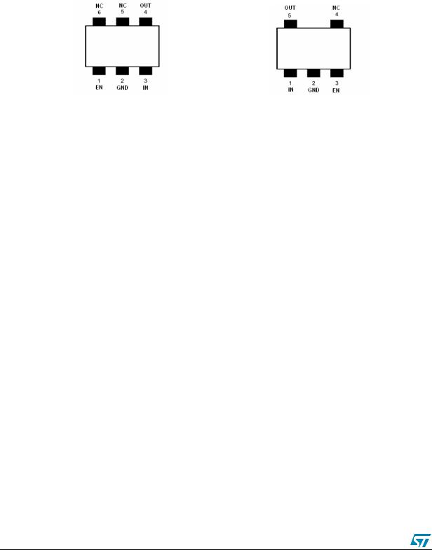
2 Pin configuration
Figure 2. Pin connection (top view)
|
|
SOT666 |
|
SOT23-5L |
|
|
|
|
|
|
|
Table 2. |
Pin description |
|
|
||
|
|
|
|
|
|
|
Pin n° |
|
Symbol |
Function |
|
|
|
|
|
||
SOT666 |
|
SOT23-5L |
|
||
|
|
|
|
||
|
|
|
|
|
|
1 |
|
3 |
|
EN |
Enable pin logic input: Low=shutdown, High=active |
|
|
|
|
|
|
2 |
|
2 |
|
GND |
Common ground. |
|
|
|
|
|
|
3 |
|
1 |
|
IN |
Input voltage of the LDO |
|
|
|
|
|
|
4 |
|
5 |
|
OUT |
Output voltage |
|
|
|
|
|
|
5 |
|
4 |
|
NC |
Not connected |
|
|
|
|
|
|
6 |
|
|
|
NC |
Not connected |
|
|
|
|
|
|
4/16
LD39015xx |
Typical application |
|
|
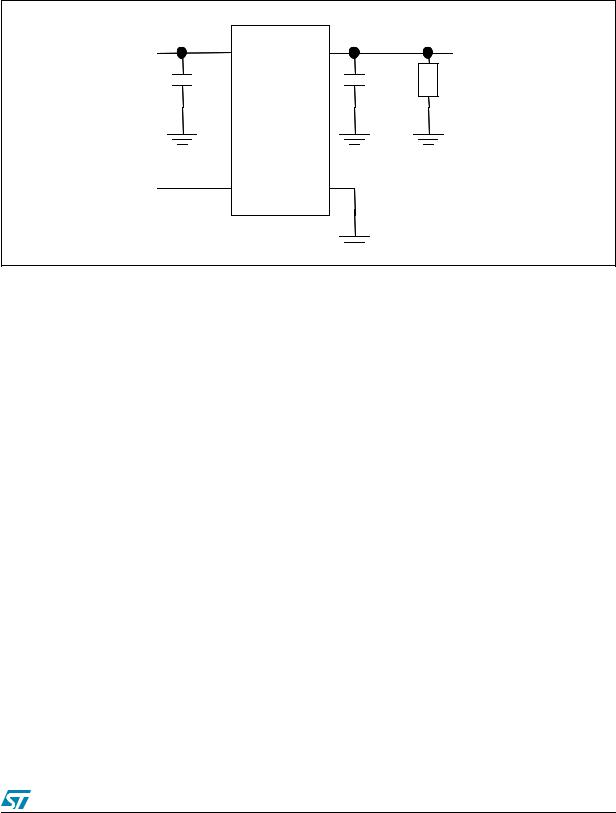
3 Typical application
Figure 3. Typical application circuit
VIN |
IN |
OUT |
|
VOUT |
1 µF |
|
|
1 µF |
Load |
VEN |
EN |
GND |
5/16
Loading...