


 Loading...
ST STM1810, STM1811, STM1812, STM1813, STM1815 User Manual
...STM1810 STM1811 STM1812 STM1813 STM1815 STM1816 STM1817 STM1818
Low power reset circuit
Features
■Precision monitoring of 3 V, 3.3 V, and 5 V supply voltages
■Four output configurations:
– Push-pull, active-high (STM1812,1817)
– Push-pull, active-low (STM1810,1815)
– Open-drain, active-low (STM1811,1816)
–Open-drain, active-low with push-button detect (STM1813,1818)
■ Reset pulse width - 100 ms (min.) |
SOT23-3 (WX) |
■Low supply current - 4 µA (typ.)
■Guaranteed assertion down to VCC = 1.0 V (0 °C to 105 °C)
■Factory-trimmed reset thresholds of 2.55 V, 2.88 V, 3.06 V, 4.37 V, and 4.62 V (typ.)
■Power supply transient immunity
■Push-button/manual reset detect (STM1813/1818)
■Operating temperature: –40 °C to 105 °C
Table 1. Device summary
■± 2.5% reset threshold accuracy: (–40 °C to 105 °C)
■Available in the SOT23-3 package
■Fully compatible with DS181x and MXD181x products.
|
|
3.3 V/ |
Active-low |
Active-low |
Active-high |
Active-low reset |
||
Order codes |
5 V |
reset |
reset |
reset |
(open-drain, |
|||
|
|
3.0 V |
|
|
|
|
|
|
|
|
(push-pull) |
(open-drain) |
(push-pull) |
bidirectional, with MR detect) |
|||
|
|
|
||||||
|
|
|
|
|
|
|
|
|
STM1810L/M |
|
|
|
|
|
|
|
|
|
|
|
|
|
|
|
|
|
STM1811L/M |
|
|
|
(1) |
|
|
|
|
STM1812L/M |
|
|
|
|
|
|
|
|
|
|
|
|
|
|
|
||
STM1813L/M |
|
|
|
|
|
|
||
|
|
|
|
|
|
|
|
|
STM1815T/S/R |
|
|
|
|
|
|
|
|
|
|
|
|
|
|
|
|
|
STM1816T/S/R |
|
|
|
(1) |
|
|
|
|
STM1817T/S/R |
|
|
|
|
|
|
|
|
|
|
|
|
|
|
|
||
STM1818T/S/R |
|
|
|
|
|
|
||
|
|
|
|
|
|
|
|
|
1. Active-low RST with internal pull-up resistor.
September 2010 |
Doc ID11464 Rev 8 |
1/25 |
www.st.com

Contents |
STM1810/1811/1812/1813/1815/1816/1817/1818 |
|
|
Contents
1 |
Description . . . . . . . . . . . . . . . . . . . . . . . . . . . . . . . . . . . . . . . . . . . . . . . . . |
5 |
|
|
1.1 |
Functional block diagrams . . . . . . . . . . . . . . . . . . . . . . . . . . . . . . . . . . . . . |
7 |
|
1.2 |
Pin descriptions . . . . . . . . . . . . . . . . . . . . . . . . . . . . . . . . . . . . . . . . . . . . . |
7 |
1.2.1 Active-low RST output (push-pull) . . . . . . . . . . . . . . . . . . . . . . . . . . . . . . 7 1.2.2 Active-low RST output (open-drain) . . . . . . . . . . . . . . . . . . . . . . . . . . . . . 7 1.2.3 Active-high RST output (push-pull) . . . . . . . . . . . . . . . . . . . . . . . . . . . . . 8
1.2.4Active-low RST output (open-drain with internal 5.5 kΩ pull-up) with
manual reset detect . . . . . . . . . . . . . . . . . . . . . . . . . . . . . . . . . . . . . . . . . 8
1.2.5 VCC . . . . . . . . . . . . . . . . . . . . . . . . . . . . . . . . . . . . . . . . . . . . . . . . . . . . . . . . . . . . . . . . . . . 8
1.2.6 VSS . . . . . . . . . . . . . . . . . . . . . . . . . . . . . . . . . . . . . . . . . . . . . . . . . . . . . . . . . . . . . . . . . . . .8
2 |
Operation . . . . . . . . . . . . . . . . . . . . . . . . . . . . . . . . . . . . . . . . . . . . . . . . . |
. 9 |
|||
|
2.1 |
Reset output . . . . . . . . . . . . . . . . . . . . . . . . . . . . . . . . . . . . . . . . . . . . . . . . |
9 |
||
|
2.2 |
Push-button detect reset (STM1813/1818) . . . . . . . . . . . . . . . . . . . . . . . . |
9 |
||
|
2.3 |
Interfacing to bidirectional microcontrollers (MCU’s) . . . . . . . . . . . . . . . . . |
9 |
||
|
2.4 |
Negative going VCC transients . . . . . . . . . . . . . . . . . . . . . . . . . . . . . . . . . . |
9 |
||
|
2.5 |
Valid |
|
output down to VCC = 0 V |
10 |
|
RST |
||||
3 |
Typical operating characteristics . . . . . . . . . . . . . . . . . . . . . . . . . . . . . |
13 |
|||
4 |
Maximum rating . . . . . . . . . . . . . . . . . . . . . . . . . . . . . . . . . . . . . . . . . . . . |
17 |
|||
5 |
DC and AC parameters . . . . . . . . . . . . . . . . . . . . . . . . . . . . . . . . . . . . . . |
18 |
|||
6 |
Package mechanical . . . . . . . . . . . . . . . . . . . . . . . . . . . . . . . . . . . . . . . . |
20 |
|||
|
6.1 |
ECOPACK® . . . . . . . . . . . . . . . . . . . . . . . . . . . . . . . . . . . . . . . . . . . . . . . . . . . . . . . . . . . . |
20 |
||
7 |
Part numbering . . . . . . . . . . . . . . . . . . . . . . . . . . . . . . . . . . . . . . . . . . . . |
22 |
|||
8 |
Revision history . . . . . . . . . . . . . . . . . . . . . . . . . . . . . . . . . . . . . . . . . . . |
24 |
|||
2/25 |
Doc ID11464 Rev 8 |

STM1810/1811/1812/1813/1815/1816/1817/1818 |
List of tables |
|
|
List of tables
Table 1. Device summary . . . . . . . . . . . . . . . . . . . . . . . . . . . . . . . . . . . . . . . . . . . . . . . . . . . . . . . . . . 1 Table 2. Signal names . . . . . . . . . . . . . . . . . . . . . . . . . . . . . . . . . . . . . . . . . . . . . . . . . . . . . . . . . . . . 6 Table 3. STM1810/STM1815 . . . . . . . . . . . . . . . . . . . . . . . . . . . . . . . . . . . . . . . . . . . . . . . . . . . . . . . 8 Table 4. STM1811/STM1816 . . . . . . . . . . . . . . . . . . . . . . . . . . . . . . . . . . . . . . . . . . . . . . . . . . . . . . . 8 Table 5. STM1812/STM1817 . . . . . . . . . . . . . . . . . . . . . . . . . . . . . . . . . . . . . . . . . . . . . . . . . . . . . . . 8 Table 6. STM1813/STM1818 . . . . . . . . . . . . . . . . . . . . . . . . . . . . . . . . . . . . . . . . . . . . . . . . . . . . . . . 8 Table 7. Absolute maximum ratings . . . . . . . . . . . . . . . . . . . . . . . . . . . . . . . . . . . . . . . . . . . . . . . . . 17 Table 8. Operating and AC measurement conditions . . . . . . . . . . . . . . . . . . . . . . . . . . . . . . . . . . . . 18 Table 9. DC and AC characteristics . . . . . . . . . . . . . . . . . . . . . . . . . . . . . . . . . . . . . . . . . . . . . . . . . 19 Table 10. SOT23-3 – 3-lead small outline transistor package mechanical data. . . . . . . . . . . . . . . . . 21 Table 11. Ordering information scheme . . . . . . . . . . . . . . . . . . . . . . . . . . . . . . . . . . . . . . . . . . . . . . . 22 Table 12. Marking description. . . . . . . . . . . . . . . . . . . . . . . . . . . . . . . . . . . . . . . . . . . . . . . . . . . . . . . 23 Table 13. Document revision history . . . . . . . . . . . . . . . . . . . . . . . . . . . . . . . . . . . . . . . . . . . . . . . . . 24
Doc ID11464 Rev 8 |
3/25 |

List of figures |
STM1810/1811/1812/1813/1815/1816/1817/1818 |
|
|
List of figures
Figure 1. Logic diagram . . . . . . . . . . . . . . . . . . . . . . . . . . . . . . . . . . . . . . . . . . . . . . . . . . . . . . . . . . . . 5 Figure 2. SOT23-3 connections . . . . . . . . . . . . . . . . . . . . . . . . . . . . . . . . . . . . . . . . . . . . . . . . . . . . . . 6 Figure 3. Hardware hookup . . . . . . . . . . . . . . . . . . . . . . . . . . . . . . . . . . . . . . . . . . . . . . . . . . . . . . . . . 6 Figure 4. Push-pull active-low output (STM1810/1812/1815/1817). . . . . . . . . . . . . . . . . . . . . . . . . . . 7 Figure 5. Open-drain, active-low output (STM1811/1816). . . . . . . . . . . . . . . . . . . . . . . . . . . . . . . . . . 7 Figure 6. Open-drain, active-low output (bidirectional, manual reset detect, STM1813/1818) . . . . . . 7 Figure 7. Reset timing diagram . . . . . . . . . . . . . . . . . . . . . . . . . . . . . . . . . . . . . . . . . . . . . . . . . . . . . 10 Figure 8. Push-button manual reset with MR detect (STM1813/1818) . . . . . . . . . . . . . . . . . . . . . . . 10 Figure 9. Manual reset timing diagram, switch bounce/debounce (STM1813/1818). . . . . . . . . . . . . 11 Figure 10. Interfacing MCUs with bidirectional reset pins (RST, open-drain, STM1811/1816) . . . . . . 11
Figure 11. Valid reset (RST) output down to VCC = 0 V (push-pull). . . . . . . . . . . . . . . . . . . . . . . . . . . 11 Figure 12. Valid reset (RST) output down to VCC = 0 V (push-pull). . . . . . . . . . . . . . . . . . . . . . . . . . . 12 Figure 13. Supply current vs. temperature (no load) . . . . . . . . . . . . . . . . . . . . . . . . . . . . . . . . . . . . . . 13
Figure 14. Normalized reset time-out period (trec) vs. temperature - VOD = VTH – VCC . . . . . . . . . . . 13 Figure 15. VCC-to-reset output delay vs. temperature - VOD = VTH – VCC . . . . . . . . . . . . . . . . . . . . . 14 Figure 16. Voltage output low vs. ISINK . . . . . . . . . . . . . . . . . . . . . . . . . . . . . . . . . . . . . . . . . . . . . . . . . . . . . . . . . . . . . 14 Figure 17. Voltage output high vs. ISOURCE . . . . . . . . . . . . . . . . . . . . . . . . . . . . . . . . . . . . . . . . . . . . . . . . . . . . . . . . . 15
Figure 18. Normalized reset threshold vs. temperature . . . . . . . . . . . . . . . . . . . . . . . . . . . . . . . . . . . . 15 Figure 19. Max. transient duration NOT causing reset pulse vs. reset threshold overdrive. . . . . . . . . 16 Figure 20. AC testing input/output waveforms . . . . . . . . . . . . . . . . . . . . . . . . . . . . . . . . . . . . . . . . . . . 18 Figure 21. SOT23-3 – 3-lead small outline transistor package outline . . . . . . . . . . . . . . . . . . . . . . . . 20
4/25 |
Doc ID11464 Rev 8 |
STM1810/1811/1812/1813/1815/1816/1817/1818 |
Description |
|
|
1 Description
STM181x devices are low power reset devices used to monitor power supplies for microcontrollers. They perform a single function: asserting a reset signal whenever VCC supply voltage drops below a preset value and keeping it asserted until VCC has risen above the preset threshold for a minimum period of time (trec). They provide excellent circuit reliability without additional external components when used with +3.0 V / +3.3 V (STM1815–STM1818), and +5 V (STM1810–STM1813) power supply systems.
A precision voltage reference and comparator monitors the VCC input for an out-of-tolerance
condition. When an invalid VCC condition occurs, the reset output (RST) is forced low (or high in the case of RST) and remains asserted for trec after VCC rises above the reset threshold. The STM1813/1818 also keep reset asserted for trec after the output is momentarily pulled to ground by an external push-button switch.
The STM1812 and STM1817 have an active-high, push-pull output. The STM1810 and STM1815 (push-pull) and STM1811, STM1813, STM1816, and STM1818 (open-drain) have an active-low RST output. The open-drain devices (STM1811 / STM1813 / STM1816 / STM1818) also have an internal pull-up resistor to VCC. The STM1813 and STM1818
feature a debounced manual reset feature that asserts a reset if the RST pin is pulled low for more than 1.5 µs. When used to initiate manual reset, RST debounces signals from devices such as mechanical switches. For devices with this feature, the release of the external switch triggers the reset period.
The STM181x devices are guaranteed to output the correct logic state for VCC down to 1.0 V (0 °C to +105 °C). They also provide a reset comparator designed to ignore fast transients on VCC.
Reset thresholds are available between +2.55 V and +4.62 V. These small, low power devices are ideal for use in portable equipment. All are available in the space-saving 3-pin SOT23 package, and are specified from –40 °C to +105 °C.
Figure 1. Logic diagram
6##
|
|
|
|
|
|
34-X |
|
|
2343 234 |
||
|
|||||
|
|
|
|
|
|
633
!)
1. For STM1812, STM1817.
Doc ID11464 Rev 8 |
5/25 |
Description |
|
|
|
|
|
STM1810/1811/1812/1813/1815/1816/1817/1818 |
|||
|
|
|
|
|
|
|
|
|
|
|
Table 2. |
Signal names |
|
|
|
||||
|
|
|
|
|
|
|
|
|
|
|
Symbol |
|
|
|
|
|
Description |
||
|
|
|
|
|
|
|
|
|
|
|
VSS |
Ground |
|
|
|
||||
|
RST |
Active-low reset output |
|
|
|
||||
|
|
|
|
|
|
|
|
|
|
|
RST(1) |
Active-high reset output |
|
|
|
||||
|
VCC |
Supply voltage and input for reset threshold monitor |
|||||||
|
1. For STM1812, STM1817. |
|
|
|
|||||
|
Figure 2. |
SOT23-3 connections |
|
|
|
||||
|
|
|
|
|
|
|
|
|
|
|
|
|
|
|
|
|
|
|
|
|
|
2343 234 |
|
|
|
633 |
|||
|
|
|
|
|
|||||
|
|
|
|
|
|
|
|
|
|
|
|
|
|
|
|
|
|
||
|
|
6## |
|
|
|
|
|
||
|
|
|
|
|
|||||
|
|
|
|
|
|
|
|
!) |
|
|
|
|
|
|
|
|
|
|
|
2. RST for STM1812 and STM1817.
Figure 3. Hardware hookup
6## 
6## |
|
6## |
||||||||||||||||||
34- X |
-#5 |
|||||||||||||||||||
|
|
|
|
|
|
|
|
|
|
|
|
2ESET |
||||||||
234 |
||||||||||||||||||||
|
|
)NPUT |
||||||||||||||||||
|
|
|
|
|
|
|
|
|
|
|
|
|||||||||
|
|
|
|
|
|
|
|
|
|
|
0USH BUTTON |
|||||||||
633 |
|
|
|
RESET |
||||||||||||||||
|
|
|
||||||||||||||||||
|
|
633 |
||||||||||||||||||
|
|
|
|
|
|
|
|
|
|
|
|
|
|
|
|
|
|
|
|
|
|
|
|
|
|
|
|
|
|
|
|
|
|
|
|
|
|
|
|
|
|
|
|
|
|
|
|
|
|
|
|
|
|
|
|
|
|
|
|
|
|
|
!) A
1.RST for STM1812 and STM1817 (see Table 1).
2.Only valid for STM1813 and STM1818.
6/25 |
Doc ID11464 Rev 8 |

STM1810/1811/1812/1813/1815/1816/1817/1818 |
Description |
|
|
1.1Functional block diagrams
Figure 4. Push-pull active-low output (STM1810/1812/1815/1817)
6## |
6234 |
#/-0!2% |
TREC |
234 |
|
GENERATOR |
|||
|
|
|
|
!) A |
1. RST for STM1812 and STM1817.
Figure 5. Open-drain, active-low output (STM1811/1816)
|
6## |
6234 |
#/-0!2% |
TREC |
234 |
|
|
GENERATOR |
|||
|
|
|
|
|
!) |
1. |
5.5 kΩ internal pull-up resistor. |
|
|
||
Figure 6. Open-drain, active-low output (bidirectional, manual reset detect,
|
|
STM1813/1818) |
|
|
|
|
|
|
|
0USH BUTTON |
|
|
|
|
|
DETECT |
234 |
|
6## |
|
|
|
|
|
6234 |
#/-0!2% |
TREC |
|
|
|
|
GENERATOR |
|
||
|
|
|
|
|
!) |
1. |
5.5 kΩ internal pull-up resistor. |
|
|
||
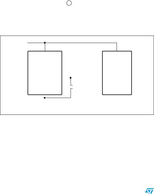
1.2Pin descriptions
See Figure 1 and Table 2 for a brief overview of the signals connected to this device.
1.2.1Active-low RST output (push-pull)
Pulses low when VCC drops below VRST, and stays low as long as VCC is below the reset threshold. It remains low for trec after VCC rises above the reset threshold.
1.2.2Active-low RST output (open-drain)
Pulses low when VCC drops below VRST, and stays low as long as VCC is below the reset threshold. It remains low for trec after VCC rises above the reset threshold. RST output has
an internal 5.5 kΩ pull-up resistor.
Doc ID11464 Rev 8 |
7/25 |

Description |
STM1810/1811/1812/1813/1815/1816/1817/1818 |
|
|
1.2.3Active-high RST output (push-pull)
Pulses high when VCC drops below VRST, and stays high as long as VCC is below the reset threshold. It remains high for trec after VCC rises above the reset threshold.
1.2.4Active-low RST output (open-drain with internal 5.5 kΩ pull-up) with manual reset detect
Pulses low when VCC drops below VRST, or RST is externally pulled low for at least 1.5 µs. It remains low for tPBRST after VCC rises above the reset threshold, or after the external manual reset is released (see Figure 9). RST output has an internal 5.5 kΩ pull-up resistor.
1.2.5VCC
Supply voltage and input for VRST comparator.
1.2.6VSS
Ground, is the reference for the power supply. It must be connected to the system ground.
Table 3. |
|
STM1810/STM1815 |
|||
Pin |
|
Name |
Function |
||
|
|
|
|
|
|
1 |
|
|
|
|
Active-low reset output (push-pull) |
|
RST |
||||
|
|
|
|
|
|
2 |
|
|
VCC |
Supply voltage and input for reset threshold monitor |
|
3 |
|
|
VSS |
Ground |
|
Table 4. |
|
STM1811/STM1816 |
|||
Pin |
|
Name |
Function |
||
|
|
|
|
|
|
1 |
|
|
|
|
Active-low reset output (open-drain, with internal 5.5 kΩ pull-up resistor) |
|
RST |
||||
|
|
|
|
|
|
2 |
|
|
VCC |
Supply voltage and input for reset threshold monitor |
|
3 |
|
|
VSS |
Ground |
|
Table 5. |
STM1812/STM1817 |
|
Pin |
Name |
Function |
|
|
|
1 |
RST |
Active-high reset output (push-pull) |
|
|
|
2 |
VCC |
Supply voltage and input for reset threshold monitor |
3 |
VSS |
Ground |
Table 6. |
|
STM1813/STM1818 |
||
Pin |
Name |
Function |
||
|
|
|
|
|
1 |
|
|
|
Active-low reset output (open-drain, with internal 5.5 kΩ pull-up) with push- |
|
RST |
|||
|
|
|
|
button/manual reset detect |
|
|
|
|
|
2 |
|
VCC |
Supply voltage and input for reset threshold monitor |
|
3 |
|
VSS |
Ground |
|
8/25 |
Doc ID11464 Rev 8 |
Loading...