


 Loading...
STGIPS10K60T
SLLIMM™ (small low-loss intelligent molded module) IPM, 3-phase inverter - 10 A, 600 V short-circuit rugged IGBT
Features
■IPM 10 A, 600 V 3-phase IGBT inverter bridge including control ICs for gate driving and freewheeling diodes
■Short-circuit rugged IGBTs
■VCE(sat) negative temperature coefficient
■3.3 V, 5 V, 15 V CMOS/TTL inputs comparators with hysteresis and pull down / pull up resistors
■Undervoltage lockout
■Internal bootstrap diode
■Interlocking function
■Shut down function
■DBC substrate leading to low thermal resistance
■Isolation rating of 2500 Vrms/min
■4.7 kΩ NTC for temperature control
Applications
■3-phase inverters for motor drives
■Home appliances, such as washing machines, refrigerators, air conditioners and sewing machines
Description
This intelligent power module provides a compact, high performance AC motor drive in a simple, rugged design. Combining ST proprietary control ICs with the most advanced short-circuit- rugged IGBT system technology, this device is ideal for 3-phase inverters in applications such as home appliances and air conditioners. SLLIMM™ is a trademark of STMicroelectronics.
SDIP-25L |
Table 1. |
Device summary |
|
|
|
|
Order code |
|
Marking |
Package |
Packaging |
|
|
|
|
|
|
|
STGIPS10K60T |
|
GIPS10K60T |
SDIP-25L |
Tube |
|
|
|
|
|
|
|
September 2011 |
Doc ID 018533 Rev 2 |
1/19 |
|||
|
|
|
|
|
|
|
|
|
|
|
www.st.com |

Contents |
STGIPS10K60T |
|
|
Contents
1 |
Internal block diagram and pin configuration . . . . . . . . . . . . . . . . . . . |
. 3 |
||
2 |
Electrical ratings . . . . . . . . . . . . . . . . . . . . . . . . . . . . . . . . . . . . . . . . . . . . |
5 |
||
|
2.1 |
Absolute maximum ratings . . . . . . . . . . . . . . . . . . . . . . . . . . . . . . . . . . . . . |
5 |
|
|
2.2 |
Thermal data . . . . . . . . . . . . . . . . . . . . . . . . . . . . . . . . . . . . . . . . . . . . . . . |
6 |
|
3 |
Electrical characteristics . . . . . . . . . . . . . . . . . . . . . . . . . . . . . . . . . . . . . |
7 |
||
|
3.1 |
Control part . . . . . . . . . . . . . . . . . . . . . . . . . . . . . . . . . . . . . . . . . . . . . . . . |
9 |
|
|
|
3.1.1 |
NTC thermistor . . . . . . . . . . . . . . . . . . . . . . . . . . . . . . . . . . . . . . . . . . . |
11 |
|
3.2 |
Waveforms definitions . . . . . . . . . . . . . . . . . . . . . . . . . . . . . . . . . . . . . . . |
12 |
|
4 |
Applications information . . . . . . . . . . . . . . . . . . . . . . . . . . . . . . . . . . . . |
13 |
||
|
4.1 |
Recommendations . . . . . . . . . . . . . . . . . . . . . . . . . . . . . . . . . . . . . . . . . . |
14 |
|
5 |
Package mechanical data . . . . . . . . . . . . . . . . . . . . . . . . . . . . . . . . . . . . |
15 |
||
6 |
Revision history . . . . . . . . . . . . . . . . . . . . . . . . . . . . . . . . . . . . . . . . . . . |
18 |
||
2/19 |
Doc ID 018533 Rev 2 |

STGIPS10K60T |
Internal block diagram and pin configuration |
|
|
1 Internal block diagram and pin configuration
Figure 1. Internal block diagram
Doc ID 018533 Rev 2 |
3/19 |
Internal block diagram and pin configuration |
STGIPS10K60T |
||||||||||
|
|
|
|
|
|
|
|
|
|
|
|
|
Table 2. |
Pin description |
|
|
|||||||
|
|
|
|
|
|
|
|||||
|
Pin n° |
|
|
Symbol |
Description |
|
|||||
|
|
|
|
|
|
|
|||||
|
1 |
|
|
OUTU |
High side reference output for U phase |
|
|||||
|
2 |
|
|
Vboot U |
Bootstrap voltage for U phase |
|
|||||
|
3 |
|
|
|
|
|
|
U |
Low side logic input for U phase |
|
|
|
|
|
LIN |
|
|||||||
|
|
|
|
|
|
|
|
||||
|
4 |
|
|
|
HINU |
High side logic input for U phase |
|
||||
|
5 |
|
|
|
VCC |
Low voltage power supply |
|
||||
|
6 |
|
|
OUTV |
High side reference output for V phase |
|
|||||
|
7 |
|
|
Vboot V |
Bootstrap voltage for V phase |
|
|||||
|
8 |
|
|
|
GND |
Ground |
|
||||
|
|
|
|
|
|
|
|
|
|
|
|
|
9 |
|
|
|
|
|
|
|
V |
Low side logic input for V phase |
|
|
|
|
LIN |
|
|||||||
|
|
|
|
|
|
|
|
||||
|
10 |
|
|
|
HINV |
High side logic input for V phase |
|
||||
|
11 |
|
|
OUTW |
High side reference output for W phase |
|
|||||
|
12 |
|
|
Vboot W |
Bootstrap voltage for W phase |
|
|||||
|
13 |
|
|
|
|
|
W |
Low side logic input for W phase |
|
||
|
|
|
LIN |
|
|||||||
|
|
|
|
|
|
|
|||||
|
14 |
|
|
HINW |
High side logic input for W phase |
|
|||||
|
15 |
|
|
|
|
/ OD |
Shut down logic input (active low) / open drain (comparator output) |
||||
SD |
|||||||||||
|
|
|
|
|
|
|
|
||||
|
16 |
|
|
|
T1 |
NTC thermistor terminal |
|
||||
|
|
|
|
|
|
|
|
||||
|
17 |
|
|
|
NW |
Negative DC input for W phase |
|
||||
|
18 |
|
|
|
W |
W phase output |
|
||||
|
|
|
|
|
|
|
|
|
|||
|
19 |
|
|
|
|
P |
Positive DC input |
|
|||
|
|
|
|
|
|
|
|
||||
|
20 |
|
|
|
NV |
Negative DC input for V phase |
|
||||
|
21 |
|
|
|
|
V |
V phase output |
|
|||
|
|
|
|
|
|
|
|
|
|||
|
22 |
|
|
|
|
P |
Positive DC input |
|
|||
|
|
|
|
|
|
|
|
||||
|
23 |
|
|
|
NU |
Negative DC input for U phase |
|
||||
|
24 |
|
|
|
|
U |
U phase output |
|
|||
|
|
|
|
|
|
|
|
|
|||
|
25 |
|
|
|
|
P |
Positive DC input |
|
|||
|
|
|
|
|
|
|
|
|
|
|
|
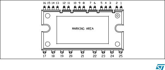
Figure 2. Pin layout (bottom view)
4/19 |
Doc ID 018533 Rev 2 |

STGIPS10K60T |
Electrical ratings |
|
|
2 Electrical ratings
2.1Absolute maximum ratings
Table 3. |
Inverter part |
|
|
|
|
|||
Symbol |
|
|
|
|
Parameter |
|
Value |
Unit |
|
|
|
|
|
|
|||
VPN |
Supply voltage applied between P - NU, NV, NW |
450 |
V |
|||||
VPN(surge) |
Supply voltage (surge) applied between P - NU, |
500 |
V |
|||||
N , N |
W |
|
|
|||||
|
V |
|
|
|
|
|||
VCES |
Each IGBT collector emitter voltage (V (1) = 0) |
600 |
V |
|||||
|
|
|
|
|
|
IN |
|
|
± I (2) |
Each IGBT continuous collector current at |
10 |
A |
|||||
|
|
|
|
|
|
|||
C |
TC = 25°C |
|
|
|
|
|||
|
|
|
|
|
||||
(3) |
Each IGBT pulsed collector current |
20 |
A |
|||||
± ICP |
||||||||
PTOT |
Each IGBT total dissipation at TC = 25°C |
33 |
W |
|||||
tscw |
Short-circuit withstand time, VCE = 0.5 V(BR)CES |
5 |
µs |
|||||
T = 125 °C, V |
= V = 15 V, V |
(1)= 5 V |
||||||
|
j |
|
CC |
boot |
IN |
|
|
|
|
|
|
|
|
|
|
|
|
1.Applied between HINi, LINi and GND for i = U, V, W.
2.Calculated according to the iterative formula:
IC(TC) |
= |
Tj(max) – TC |
|
× VCE-----------------(sat)(max-----------------)(T-----------------j(max),-----------------IC(TC---))- |
|||
|
Rthj – c |
3. Pulse width limited by max junction temperature.
Table 4. |
Control part |
|
|
|||||
Symbol |
Parameter |
Value |
Unit |
|||||
|
|
|
|
|
|
|||
VOUT |
Output voltage applied between |
Vboot - 21 to Vboot + 0.3 |
V |
|||||
OUTU, OUTV, OUTW - GND |
||||||||
|
|
|
|
|
||||
|
VCC |
Low voltage power supply |
-0.3 to +21 |
V |
||||
Vboot |
Bootstrap voltage applied between |
-0.3 to 620 |
V |
|||||
Vboot i - OUTi for i = U, V, W |
||||||||
|
|
|
|
|
||||
|
|
|
Logic input voltage applied between HIN, |
|
and |
|
|
|
|
VIN |
LIN |
-0.3 to 15 |
V |
||||
|
GND |
|||||||
V |
|
|
Open drain voltage |
-0.3 to 15 |
V |
|||
SD/OD |
||||||||
dVOUT/dt |
Allowed output slew rate |
50 |
V/ns |
|||||
Doc ID 018533 Rev 2 |
5/19 |

Electrical ratings |
|
STGIPS10K60T |
||
|
|
|
|
|
|
Table 5. |
Total system |
|
|
|
|
|
|
|
|
Symbol |
Parameter |
Value |
Unit |
|
|
|
|
|
|
VISO |
Isolation withstand voltage applied between each |
2500 |
V |
|
pin and heatsink plate (AC voltage, t = 60 sec.) |
|||
|
TC |
Module case operation temperature |
-40 to 125 |
°C |
|
TJ (1) |
Operating junction temperature |
-40 to 150 |
°C |
1.The maximum junction temperature rating of the power chips integrated within the SDIP module is 150°C (@TC ≤ 100°C). To ensure safe operation of the SDIP module, the average junction temperature should be limited to TJ(avg) ≤ 125°C (@TC ≤ 100°C)
2.2Thermal data
Table 6. |
Thermal data |
|
|
|
Symbol |
Parameter |
Value |
Unit |
|
|
|
|
|
|
RthJC |
Thermal resistance junction-case single IGBT max. |
3.8 |
°C/W |
|
|
|
|
||
Thermal resistance junction-case single diode max. |
5.5 |
°C/W |
||
|
||||
|
|
|
|
6/19 |
Doc ID 018533 Rev 2 |
Loading...