


ST72324BK2
Table of contents
 Loading...
ST ST72324BK2, ST72324BK4, ST72324BK6, ST72324BJ2, ST72324BJ4 User Manual
...
8-bit MCU for automotive, 3.8 to 5.5V operating range with
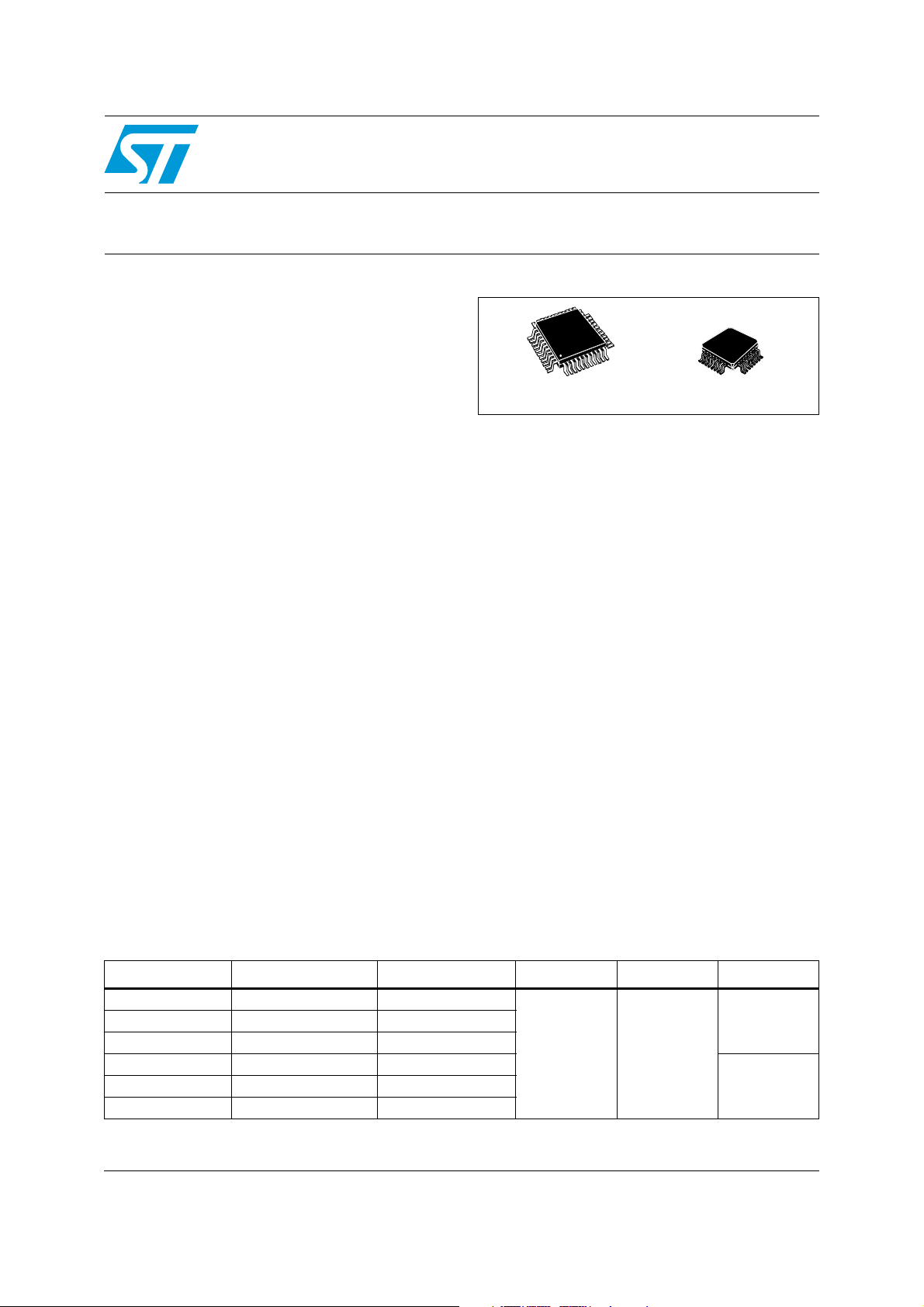
LQFP44
10 x 10
LQFP32
7 x 7
8 to 32 Kbyte Flash/ROM, 10-bit ADC, 4 timers, SPI, SCI
Features
Memories
■ 8 to 32 Kbyte dual voltage High Density Flash
(HDFlash) or ROM with readout protection
capability. In-application programming and Incircuit programming for HDFlash devices
■ 384 bytes to 1 Kbyte RAM
■ HDFlash endurance: 100 cycles, data retention
20 years
Clock, reset and supply management
■ Enhanced low voltage supervisor (LVD) with
programmable reset thresholds and auxiliary
voltage detector (AVD) with interrupt capability
■ Clock sources: crystal/ceramic resonator
oscillators, internal RC oscillator and external
clock input
■ PLL for 2x frequency multiplication
■ 4 power saving modes: Slow, Wait, Active Halt,
and Halt
ST72324Bxx-Auto
4 timers
■ Main clock controller with Real-time base,
Beep and Clock-out capabilities
■ Configurable watchdog timer
■ 16-bit Timer A with 1 input capture, 1 output
compare, external clock input, PWM and pulse
generator modes
■ 16-bit Timer B with 2 input captures, 2 output
compares, PWM and pulse generator modes
2 communication interfaces
■ SPI synchronous serial interface
■ SCI asynchronous serial interface
Interrupt management
■ Nested interrupt controller
■ 10 interrupt vectors plus TRAP and RESET
■ 9/6 external interrupt lines (on 4 vectors)
Up to 32 I/O ports
■ 32/24 multifunctional bidirectional I/O lines
■ 22/17 alternate function lines
■ 12/10 high sink outputs
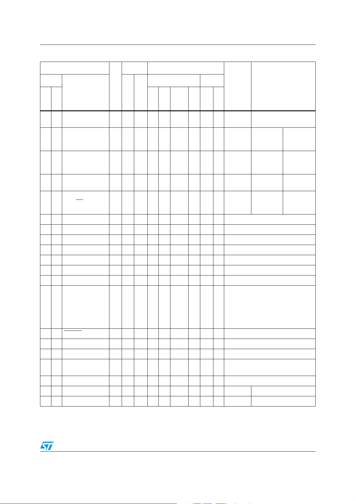
Table 1. Device summary
Device Memory RAM (stack) Voltage range Temp. range Package
ST72324BK2-Auto Flash/ROM 8 Kbytes 384 (256) bytes
ST72324BK4-Auto Flash/ROM 16 Kbytes 512 (256) bytes
ST72324BK6-Auto Flash/ROM 32 Kbytes 1024 (256) bytes
ST72324BJ2-Auto Flash/ROM 8 Kbytes 384 (256) bytes
ST72324BJ4-Auto Flash/ROM 16 Kbytes 512 (256) bytes
ST72324BJ6-Auto Flash/ROM 32 Kbytes 1024 (256) bytes
1 analog peripheral (low current coupling)
■ 10-bit ADC with up to 12 input ports
Instruction set
■ 8-bit data manipulation
■ 63 basic instructions
■ 17 main addressing modes
■ 8 x 8 Unsigned Multiply Instruction
Development tools
■ In-circuit testing capability
3.8 to 5.5V
up to
-40 to 125°C
LQFP32
7x7
LQFP44
10x10
July 2010 Doc ID13466 Rev 4 1/198
www.st.com
1

Contents ST72324B-Auto
Contents
1 Description . . . . . . . . . . . . . . . . . . . . . . . . . . . . . . . . . . . . . . . . . . . . . . . . 14
2 Pin description . . . . . . . . . . . . . . . . . . . . . . . . . . . . . . . . . . . . . . . . . . . . 15
3 Register and memory map . . . . . . . . . . . . . . . . . . . . . . . . . . . . . . . . . . . 19
4 Flash program memory . . . . . . . . . . . . . . . . . . . . . . . . . . . . . . . . . . . . . 22
4.1 Introduction . . . . . . . . . . . . . . . . . . . . . . . . . . . . . . . . . . . . . . . . . . . . . . . 22
4.2 Main features . . . . . . . . . . . . . . . . . . . . . . . . . . . . . . . . . . . . . . . . . . . . . . 22
4.3 Structure . . . . . . . . . . . . . . . . . . . . . . . . . . . . . . . . . . . . . . . . . . . . . . . . . . 22
4.3.1 Readout protection . . . . . . . . . . . . . . . . . . . . . . . . . . . . . . . . . . . . . . . . 23
4.4 ICC interface . . . . . . . . . . . . . . . . . . . . . . . . . . . . . . . . . . . . . . . . . . . . . . 23
4.5 ICP (in-circuit programming) . . . . . . . . . . . . . . . . . . . . . . . . . . . . . . . . . . 24
4.6 IAP (in-application programming) . . . . . . . . . . . . . . . . . . . . . . . . . . . . . . . 25
4.7 Related documentation . . . . . . . . . . . . . . . . . . . . . . . . . . . . . . . . . . . . . . 25
4.7.1 Flash Control/Status Register (FCSR) . . . . . . . . . . . . . . . . . . . . . . . . . . 25
5 Central processing unit (CPU) . . . . . . . . . . . . . . . . . . . . . . . . . . . . . . . . 26
5.1 Introduction . . . . . . . . . . . . . . . . . . . . . . . . . . . . . . . . . . . . . . . . . . . . . . . 26
5.2 Main features . . . . . . . . . . . . . . . . . . . . . . . . . . . . . . . . . . . . . . . . . . . . . . 26
5.3 CPU registers . . . . . . . . . . . . . . . . . . . . . . . . . . . . . . . . . . . . . . . . . . . . . . 26
5.3.1 Accumulator (A) . . . . . . . . . . . . . . . . . . . . . . . . . . . . . . . . . . . . . . . . . . . 27
5.3.2 Index registers (X and Y) . . . . . . . . . . . . . . . . . . . . . . . . . . . . . . . . . . . . 27
5.3.3 Program counter (PC) . . . . . . . . . . . . . . . . . . . . . . . . . . . . . . . . . . . . . . 27
5.3.4 Condition Code register (CC) . . . . . . . . . . . . . . . . . . . . . . . . . . . . . . . . 27
5.3.5 Stack Pointer register (SP) . . . . . . . . . . . . . . . . . . . . . . . . . . . . . . . . . . 29
6 Supply, reset and clock management . . . . . . . . . . . . . . . . . . . . . . . . . . 31
6.1 Introduction . . . . . . . . . . . . . . . . . . . . . . . . . . . . . . . . . . . . . . . . . . . . . . . 31
6.2 PLL (phase locked loop) . . . . . . . . . . . . . . . . . . . . . . . . . . . . . . . . . . . . . . 31
6.3 Multi-oscillator (MO) . . . . . . . . . . . . . . . . . . . . . . . . . . . . . . . . . . . . . . . . . 32
6.3.1 External clock source . . . . . . . . . . . . . . . . . . . . . . . . . . . . . . . . . . . . . . . 32
6.3.2 Crystal/ceramic oscillators . . . . . . . . . . . . . . . . . . . . . . . . . . . . . . . . . . . 33
2/198 Doc ID13466 Rev 4

ST72324B-Auto Contents
6.3.3 Internal RC oscillator . . . . . . . . . . . . . . . . . . . . . . . . . . . . . . . . . . . . . . . 33
6.4 Reset sequence manager (RSM) . . . . . . . . . . . . . . . . . . . . . . . . . . . . . . . 34
6.4.1 Asynchronous external RESET pin . . . . . . . . . . . . . . . . . . . . . . . . . . . . 34
6.5 System integrity management (SI) . . . . . . . . . . . . . . . . . . . . . . . . . . . . . . 36
6.5.1 LVD (low voltage detector) . . . . . . . . . . . . . . . . . . . . . . . . . . . . . . . . . . . 36
6.5.2 AVD (auxiliary voltage detector) . . . . . . . . . . . . . . . . . . . . . . . . . . . . . . 37
6.5.3 Low power modes . . . . . . . . . . . . . . . . . . . . . . . . . . . . . . . . . . . . . . . . . 38
6.5.4 Interrupts . . . . . . . . . . . . . . . . . . . . . . . . . . . . . . . . . . . . . . . . . . . . . . . . 38
6.6 SI registers . . . . . . . . . . . . . . . . . . . . . . . . . . . . . . . . . . . . . . . . . . . . . . . . 39
6.6.1 System integrity (SI) control/status register (SICSR) . . . . . . . . . . . . . . . 39
7 Interrupts . . . . . . . . . . . . . . . . . . . . . . . . . . . . . . . . . . . . . . . . . . . . . . . . . 41
7.1 Introduction . . . . . . . . . . . . . . . . . . . . . . . . . . . . . . . . . . . . . . . . . . . . . . . 41
7.2 Masking and processing flow . . . . . . . . . . . . . . . . . . . . . . . . . . . . . . . . . . 41
7.2.1 Servicing pending interrupts . . . . . . . . . . . . . . . . . . . . . . . . . . . . . . . . . 42
7.2.2 Different interrupt vector sources . . . . . . . . . . . . . . . . . . . . . . . . . . . . . . 43
7.2.3 Non-maskable sources . . . . . . . . . . . . . . . . . . . . . . . . . . . . . . . . . . . . . 43
7.2.4 Maskable sources . . . . . . . . . . . . . . . . . . . . . . . . . . . . . . . . . . . . . . . . . 43
7.3 Interrupts and low power modes . . . . . . . . . . . . . . . . . . . . . . . . . . . . . . . 44
7.4 Concurrent and nested management . . . . . . . . . . . . . . . . . . . . . . . . . . . . 44
7.5 Interrupt registers . . . . . . . . . . . . . . . . . . . . . . . . . . . . . . . . . . . . . . . . . . . 45
7.5.1 CPU CC register interrupt bits . . . . . . . . . . . . . . . . . . . . . . . . . . . . . . . . 45
7.5.2 Interrupt software priority registers (ISPRx) . . . . . . . . . . . . . . . . . . . . . . 46
7.6 External interrupts . . . . . . . . . . . . . . . . . . . . . . . . . . . . . . . . . . . . . . . . . . 48
7.6.1 I/O port interrupt sensitivity . . . . . . . . . . . . . . . . . . . . . . . . . . . . . . . . . . 48
7.6.2 External interrupt control register (EICR) . . . . . . . . . . . . . . . . . . . . . . . . 49
8 Power saving modes . . . . . . . . . . . . . . . . . . . . . . . . . . . . . . . . . . . . . . . . 52
8.1 Introduction . . . . . . . . . . . . . . . . . . . . . . . . . . . . . . . . . . . . . . . . . . . . . . . 52
8.2 Slow mode . . . . . . . . . . . . . . . . . . . . . . . . . . . . . . . . . . . . . . . . . . . . . . . . 52
8.3 Wait mode . . . . . . . . . . . . . . . . . . . . . . . . . . . . . . . . . . . . . . . . . . . . . . . . 53
8.4 Active Halt and Halt modes . . . . . . . . . . . . . . . . . . . . . . . . . . . . . . . . . . . 54
8.4.1 Active Halt mode . . . . . . . . . . . . . . . . . . . . . . . . . . . . . . . . . . . . . . . . . . 54
8.4.2 Halt mode . . . . . . . . . . . . . . . . . . . . . . . . . . . . . . . . . . . . . . . . . . . . . . . 55
9 I/O ports . . . . . . . . . . . . . . . . . . . . . . . . . . . . . . . . . . . . . . . . . . . . . . . . . . 58
Doc ID13466 Rev 4 3/198

Contents ST72324B-Auto
9.1 Introduction . . . . . . . . . . . . . . . . . . . . . . . . . . . . . . . . . . . . . . . . . . . . . . . 58
9.2 Functional description . . . . . . . . . . . . . . . . . . . . . . . . . . . . . . . . . . . . . . . 58
9.2.1 Input modes . . . . . . . . . . . . . . . . . . . . . . . . . . . . . . . . . . . . . . . . . . . . . . 58
9.2.2 Output modes . . . . . . . . . . . . . . . . . . . . . . . . . . . . . . . . . . . . . . . . . . . . 59
9.2.3 Alternate functions . . . . . . . . . . . . . . . . . . . . . . . . . . . . . . . . . . . . . . . . . 59
9.3 I/O port implementation . . . . . . . . . . . . . . . . . . . . . . . . . . . . . . . . . . . . . . 62
9.4 Low power modes . . . . . . . . . . . . . . . . . . . . . . . . . . . . . . . . . . . . . . . . . . 62
9.5 Interrupts . . . . . . . . . . . . . . . . . . . . . . . . . . . . . . . . . . . . . . . . . . . . . . . . . 62
9.5.1 I/O port implementation . . . . . . . . . . . . . . . . . . . . . . . . . . . . . . . . . . . . . 63
10 On-chip peripherals . . . . . . . . . . . . . . . . . . . . . . . . . . . . . . . . . . . . . . . . 65
10.1 Watchdog timer (WDG) . . . . . . . . . . . . . . . . . . . . . . . . . . . . . . . . . . . . . . 65
10.1.1 Introduction . . . . . . . . . . . . . . . . . . . . . . . . . . . . . . . . . . . . . . . . . . . . . . 65
10.1.2 Main features . . . . . . . . . . . . . . . . . . . . . . . . . . . . . . . . . . . . . . . . . . . . . 65
10.1.3 Functional description . . . . . . . . . . . . . . . . . . . . . . . . . . . . . . . . . . . . . . 65
10.1.4 How to program the Watchdog timeout . . . . . . . . . . . . . . . . . . . . . . . . . 66
10.1.5 Low power modes . . . . . . . . . . . . . . . . . . . . . . . . . . . . . . . . . . . . . . . . . 68
10.1.6 Hardware Watchdog option . . . . . . . . . . . . . . . . . . . . . . . . . . . . . . . . . . 68
10.1.7 Using Halt mode with the WDG (WDGHALT option) . . . . . . . . . . . . . . . 68
10.1.8 Interrupts . . . . . . . . . . . . . . . . . . . . . . . . . . . . . . . . . . . . . . . . . . . . . . . . 68
10.1.9 Control register (WDGCR) . . . . . . . . . . . . . . . . . . . . . . . . . . . . . . . . . . . 69
10.2 Main clock controller with real-time clock and beeper (MCC/RTC) . . . . . 69
10.2.1 Programmable CPU clock prescaler . . . . . . . . . . . . . . . . . . . . . . . . . . . 69
10.2.2 Clock-out capability . . . . . . . . . . . . . . . . . . . . . . . . . . . . . . . . . . . . . . . . 70
10.2.3 Real-time clock (RTC) timer . . . . . . . . . . . . . . . . . . . . . . . . . . . . . . . . . . 70
10.2.4 Beeper . . . . . . . . . . . . . . . . . . . . . . . . . . . . . . . . . . . . . . . . . . . . . . . . . . 70
10.2.5 Low power modes . . . . . . . . . . . . . . . . . . . . . . . . . . . . . . . . . . . . . . . . . 71
10.2.6 Interrupts . . . . . . . . . . . . . . . . . . . . . . . . . . . . . . . . . . . . . . . . . . . . . . . . 71
10.2.7 MCC registers . . . . . . . . . . . . . . . . . . . . . . . . . . . . . . . . . . . . . . . . . . . . 71
10.3 16-bit timer . . . . . . . . . . . . . . . . . . . . . . . . . . . . . . . . . . . . . . . . . . . . . . . . 74
10.3.1 Introduction . . . . . . . . . . . . . . . . . . . . . . . . . . . . . . . . . . . . . . . . . . . . . . 74
10.3.2 Main features . . . . . . . . . . . . . . . . . . . . . . . . . . . . . . . . . . . . . . . . . . . . . 74
10.3.3 Functional description . . . . . . . . . . . . . . . . . . . . . . . . . . . . . . . . . . . . . . 75
10.3.4 Low power modes . . . . . . . . . . . . . . . . . . . . . . . . . . . . . . . . . . . . . . . . . 88
10.3.5 Interrupts . . . . . . . . . . . . . . . . . . . . . . . . . . . . . . . . . . . . . . . . . . . . . . . . 88
10.3.6 Summary of timer modes . . . . . . . . . . . . . . . . . . . . . . . . . . . . . . . . . . . . 89
4/198 Doc ID13466 Rev 4

ST72324B-Auto Contents
10.3.7 16-bit timer registers . . . . . . . . . . . . . . . . . . . . . . . . . . . . . . . . . . . . . . . 89
10.4 Serial peripheral interface (SPI) . . . . . . . . . . . . . . . . . . . . . . . . . . . . . . . . 97
10.4.1 Introduction . . . . . . . . . . . . . . . . . . . . . . . . . . . . . . . . . . . . . . . . . . . . . . 97
10.4.2 Main features . . . . . . . . . . . . . . . . . . . . . . . . . . . . . . . . . . . . . . . . . . . . . 97
10.4.3 General description . . . . . . . . . . . . . . . . . . . . . . . . . . . . . . . . . . . . . . . . 98
10.4.4 Clock phase and clock polarity . . . . . . . . . . . . . . . . . . . . . . . . . . . . . . 102
10.4.5 Error flags . . . . . . . . . . . . . . . . . . . . . . . . . . . . . . . . . . . . . . . . . . . . . . 103
10.4.6 Low power modes . . . . . . . . . . . . . . . . . . . . . . . . . . . . . . . . . . . . . . . . 105
10.4.7 Interrupts . . . . . . . . . . . . . . . . . . . . . . . . . . . . . . . . . . . . . . . . . . . . . . . 105
10.4.8 SPI registers . . . . . . . . . . . . . . . . . . . . . . . . . . . . . . . . . . . . . . . . . . . . 106
10.5 Serial communications interface (SCI) . . . . . . . . . . . . . . . . . . . . . . . . . . 110
10.5.1 Introduction . . . . . . . . . . . . . . . . . . . . . . . . . . . . . . . . . . . . . . . . . . . . . 110
10.5.2 Main features . . . . . . . . . . . . . . . . . . . . . . . . . . . . . . . . . . . . . . . . . . . . 110
10.5.3 General description . . . . . . . . . . . . . . . . . . . . . . . . . . . . . . . . . . . . . . . 111
10.5.4 Functional description . . . . . . . . . . . . . . . . . . . . . . . . . . . . . . . . . . . . . 113
10.5.5 Low power modes . . . . . . . . . . . . . . . . . . . . . . . . . . . . . . . . . . . . . . . . 122
10.5.6 Interrupts . . . . . . . . . . . . . . . . . . . . . . . . . . . . . . . . . . . . . . . . . . . . . . . 122
10.5.7 SCI registers . . . . . . . . . . . . . . . . . . . . . . . . . . . . . . . . . . . . . . . . . . . . 122
10.6 10-bit A/D converter (ADC) . . . . . . . . . . . . . . . . . . . . . . . . . . . . . . . . . . 131
10.6.1 Introduction . . . . . . . . . . . . . . . . . . . . . . . . . . . . . . . . . . . . . . . . . . . . . 131
10.6.2 Main features . . . . . . . . . . . . . . . . . . . . . . . . . . . . . . . . . . . . . . . . . . . . 131
10.6.3 Functional description . . . . . . . . . . . . . . . . . . . . . . . . . . . . . . . . . . . . . 132
10.6.4 Low power modes . . . . . . . . . . . . . . . . . . . . . . . . . . . . . . . . . . . . . . . . 133
10.6.5 Interrupts . . . . . . . . . . . . . . . . . . . . . . . . . . . . . . . . . . . . . . . . . . . . . . . 133
10.6.6 ADC registers . . . . . . . . . . . . . . . . . . . . . . . . . . . . . . . . . . . . . . . . . . . 133
11 Instruction set . . . . . . . . . . . . . . . . . . . . . . . . . . . . . . . . . . . . . . . . . . . . 136
11.1 CPU addressing modes . . . . . . . . . . . . . . . . . . . . . . . . . . . . . . . . . . . . . 136
11.1.1 Inherent . . . . . . . . . . . . . . . . . . . . . . . . . . . . . . . . . . . . . . . . . . . . . . . . 137
11.1.2 Immediate . . . . . . . . . . . . . . . . . . . . . . . . . . . . . . . . . . . . . . . . . . . . . . 138
11.1.3 Direct . . . . . . . . . . . . . . . . . . . . . . . . . . . . . . . . . . . . . . . . . . . . . . . . . . 138
11.1.4 Indexed (no offset, short, long) . . . . . . . . . . . . . . . . . . . . . . . . . . . . . . 138
11.1.5 Indirect (short, long) . . . . . . . . . . . . . . . . . . . . . . . . . . . . . . . . . . . . . . . 139
11.1.6 Indirect indexed (short, long) . . . . . . . . . . . . . . . . . . . . . . . . . . . . . . . . 139
11.1.7 Relative mode (direct, indirect) . . . . . . . . . . . . . . . . . . . . . . . . . . . . . . 140
11.2 Instruction groups . . . . . . . . . . . . . . . . . . . . . . . . . . . . . . . . . . . . . . . . . . 140
Doc ID13466 Rev 4 5/198

Contents ST72324B-Auto
12 Electrical characteristics . . . . . . . . . . . . . . . . . . . . . . . . . . . . . . . . . . . 145
12.1 Parameter conditions . . . . . . . . . . . . . . . . . . . . . . . . . . . . . . . . . . . . . . . 145
12.1.1 Minimum and maximum values . . . . . . . . . . . . . . . . . . . . . . . . . . . . . . 145
12.1.2 Typical values . . . . . . . . . . . . . . . . . . . . . . . . . . . . . . . . . . . . . . . . . . . . 145
12.1.3 Typical curves . . . . . . . . . . . . . . . . . . . . . . . . . . . . . . . . . . . . . . . . . . . 145
12.1.4 Loading capacitor . . . . . . . . . . . . . . . . . . . . . . . . . . . . . . . . . . . . . . . . 145
12.1.5 Pin input voltage . . . . . . . . . . . . . . . . . . . . . . . . . . . . . . . . . . . . . . . . . 146
12.2 Absolute maximum ratings . . . . . . . . . . . . . . . . . . . . . . . . . . . . . . . . . . . 146
12.2.1 Voltage characteristics . . . . . . . . . . . . . . . . . . . . . . . . . . . . . . . . . . . . . 146
12.2.2 Current characteristics . . . . . . . . . . . . . . . . . . . . . . . . . . . . . . . . . . . . . 147
12.2.3 Thermal characteristics . . . . . . . . . . . . . . . . . . . . . . . . . . . . . . . . . . . . 147
12.3 Operating conditions . . . . . . . . . . . . . . . . . . . . . . . . . . . . . . . . . . . . . . . 148
12.4 LVD/AVD characteristics . . . . . . . . . . . . . . . . . . . . . . . . . . . . . . . . . . . . . 149
12.4.1 Operating conditions with LVD . . . . . . . . . . . . . . . . . . . . . . . . . . . . . . . 149
12.4.2 Auxiliary voltage detector (AVD) thresholds . . . . . . . . . . . . . . . . . . . . . 149
12.5 Supply current characteristics . . . . . . . . . . . . . . . . . . . . . . . . . . . . . . . . 150
12.5.1 ROM current consumption . . . . . . . . . . . . . . . . . . . . . . . . . . . . . . . . . . 150
12.5.2 Flash current consumption . . . . . . . . . . . . . . . . . . . . . . . . . . . . . . . . . 151
12.5.3 Supply and clock managers . . . . . . . . . . . . . . . . . . . . . . . . . . . . . . . . . 152
12.5.4 On-chip peripherals . . . . . . . . . . . . . . . . . . . . . . . . . . . . . . . . . . . . . . . 152
12.6 Clock and timing characteristics . . . . . . . . . . . . . . . . . . . . . . . . . . . . . . . 153
12.6.1 General timings . . . . . . . . . . . . . . . . . . . . . . . . . . . . . . . . . . . . . . . . . . 153
12.6.2 External clock source . . . . . . . . . . . . . . . . . . . . . . . . . . . . . . . . . . . . . . 153
12.6.3 Crystal and ceramic resonator oscillators . . . . . . . . . . . . . . . . . . . . . . 154
12.6.4 RC oscillators . . . . . . . . . . . . . . . . . . . . . . . . . . . . . . . . . . . . . . . . . . . . 155
12.6.5 PLL characteristics . . . . . . . . . . . . . . . . . . . . . . . . . . . . . . . . . . . . . . . 156
12.7 Memory characteristics . . . . . . . . . . . . . . . . . . . . . . . . . . . . . . . . . . . . . 156
12.7.1 RAM and hardware registers . . . . . . . . . . . . . . . . . . . . . . . . . . . . . . . . 156
12.7.2 Flash memory . . . . . . . . . . . . . . . . . . . . . . . . . . . . . . . . . . . . . . . . . . . 157
12.8 EMC characteristics . . . . . . . . . . . . . . . . . . . . . . . . . . . . . . . . . . . . . . . . 158
12.8.1 Functional electromagnetic susceptibility (EMS) . . . . . . . . . . . . . . . . . 158
12.8.2 Electromagnetic interference (EMI) . . . . . . . . . . . . . . . . . . . . . . . . . . . 159
12.8.3 Absolute maximum ratings (electrical sensitivity) . . . . . . . . . . . . . . . . 160
12.9 I/O port pin characteristics . . . . . . . . . . . . . . . . . . . . . . . . . . . . . . . . . . . 162
12.9.1 General characteristics . . . . . . . . . . . . . . . . . . . . . . . . . . . . . . . . . . . . 162
12.9.2 Output driving current . . . . . . . . . . . . . . . . . . . . . . . . . . . . . . . . . . . . . 163
6/198 Doc ID13466 Rev 4

ST72324B-Auto Contents
12.10 Control pin characteristics . . . . . . . . . . . . . . . . . . . . . . . . . . . . . . . . . . . 166
12.10.1 Asynchronous RESET pin . . . . . . . . . . . . . . . . . . . . . . . . . . . . . . . . . . 166
12.10.2 ICCSEL/VPP pin . . . . . . . . . . . . . . . . . . . . . . . . . . . . . . . . . . . . . . . . . 168
12.11 Timer peripheral characteristics . . . . . . . . . . . . . . . . . . . . . . . . . . . . . . . 168
12.11.1 16-bit timer . . . . . . . . . . . . . . . . . . . . . . . . . . . . . . . . . . . . . . . . . . . . . . 168
12.12 Communication interface characteristics . . . . . . . . . . . . . . . . . . . . . . . . 169
12.12.1 Serial peripheral interface (SPI) . . . . . . . . . . . . . . . . . . . . . . . . . . . . . . 169
12.13 10-bit ADC characteristics . . . . . . . . . . . . . . . . . . . . . . . . . . . . . . . . . . . 171
12.13.1 Analog power supply and reference pins . . . . . . . . . . . . . . . . . . . . . . . 173
12.13.2 General PCB design guidelines . . . . . . . . . . . . . . . . . . . . . . . . . . . . . . 173
12.13.3 ADC accuracy . . . . . . . . . . . . . . . . . . . . . . . . . . . . . . . . . . . . . . . . . . . 174
13 Package characteristics . . . . . . . . . . . . . . . . . . . . . . . . . . . . . . . . . . . . 175
13.1 LQFP44 package characteristics . . . . . . . . . . . . . . . . . . . . . . . . . . . . . . 175
13.2 LQFP32 package characteristics . . . . . . . . . . . . . . . . . . . . . . . . . . . . . . 176
13.3 Thermal characteristics . . . . . . . . . . . . . . . . . . . . . . . . . . . . . . . . . . . . . 178
13.4 Ecopack information . . . . . . . . . . . . . . . . . . . . . . . . . . . . . . . . . . . . . . . . 178
13.5 Packaging for automatic handling . . . . . . . . . . . . . . . . . . . . . . . . . . . . . 178
14 Device configuration and ordering information . . . . . . . . . . . . . . . . . 179
14.1 Flash devices . . . . . . . . . . . . . . . . . . . . . . . . . . . . . . . . . . . . . . . . . . . . . 179
14.1.1 Flash configuration . . . . . . . . . . . . . . . . . . . . . . . . . . . . . . . . . . . . . . . 179
14.1.2 Flash ordering information . . . . . . . . . . . . . . . . . . . . . . . . . . . . . . . . . . 182
14.2 ROM device ordering information and transfer of customer code . . . . . 183
14.3 Development tools . . . . . . . . . . . . . . . . . . . . . . . . . . . . . . . . . . . . . . . . . 187
14.3.1 Introduction . . . . . . . . . . . . . . . . . . . . . . . . . . . . . . . . . . . . . . . . . . . . . 187
14.3.2 Evaluation tools and starter kits . . . . . . . . . . . . . . . . . . . . . . . . . . . . . . 187
14.3.3 Development and debugging tools . . . . . . . . . . . . . . . . . . . . . . . . . . . 187
14.3.4 Programming tools . . . . . . . . . . . . . . . . . . . . . . . . . . . . . . . . . . . . . . . . 187
14.3.5 Socket and emulator adapter information . . . . . . . . . . . . . . . . . . . . . . 188
14.4 ST7 Application notes . . . . . . . . . . . . . . . . . . . . . . . . . . . . . . . . . . . . . . 188
15 Known limitations . . . . . . . . . . . . . . . . . . . . . . . . . . . . . . . . . . . . . . . . . 189
15.1 All Flash and ROM devices . . . . . . . . . . . . . . . . . . . . . . . . . . . . . . . . . . 189
15.1.1 Safe connection of OSC1/OSC2 pins . . . . . . . . . . . . . . . . . . . . . . . . . 189
15.1.2 External interrupt missed . . . . . . . . . . . . . . . . . . . . . . . . . . . . . . . . . . . 189
Doc ID13466 Rev 4 7/198

Contents ST72324B-Auto
15.1.3 Unexpected reset fetch . . . . . . . . . . . . . . . . . . . . . . . . . . . . . . . . . . . . 191
15.1.4 Clearing active interrupts outside interrupt routine . . . . . . . . . . . . . . . 191
15.1.5 16-bit timer PWM mode . . . . . . . . . . . . . . . . . . . . . . . . . . . . . . . . . . . . 192
15.1.6 TIMD set simultaneously with OC interrupt . . . . . . . . . . . . . . . . . . . . . 192
15.1.7 SCI wrong break duration . . . . . . . . . . . . . . . . . . . . . . . . . . . . . . . . . . 192
15.2 8/16 Kbyte Flash devices only . . . . . . . . . . . . . . . . . . . . . . . . . . . . . . . . 193
15.2.1 39-pulse ICC entry mode . . . . . . . . . . . . . . . . . . . . . . . . . . . . . . . . . . . 193
15.2.2 Negative current injection on pin PB0 . . . . . . . . . . . . . . . . . . . . . . . . . 193
15.3 8/16 Kbyte ROM devices only . . . . . . . . . . . . . . . . . . . . . . . . . . . . . . . . 193
15.3.1 Readout protection with LVD . . . . . . . . . . . . . . . . . . . . . . . . . . . . . . . . 193
15.3.2 I/O Port A and F configuration . . . . . . . . . . . . . . . . . . . . . . . . . . . . . . . 193
16 Revision history . . . . . . . . . . . . . . . . . . . . . . . . . . . . . . . . . . . . . . . . . . 195
8/198 Doc ID13466 Rev 4

ST72324B-Auto List of tables
List of tables
Table 1. Device summary. . . . . . . . . . . . . . . . . . . . . . . . . . . . . . . . . . . . . . . . . . . . . . . . . . . . . . . . . . 1
Table 2. Device pin description. . . . . . . . . . . . . . . . . . . . . . . . . . . . . . . . . . . . . . . . . . . . . . . . . . . . . 16
Table 3. Hardware register map . . . . . . . . . . . . . . . . . . . . . . . . . . . . . . . . . . . . . . . . . . . . . . . . . . . . 19
Table 4. Sectors available in Flash devices . . . . . . . . . . . . . . . . . . . . . . . . . . . . . . . . . . . . . . . . . . . 22
Table 5. Flash control/status register address and reset value . . . . . . . . . . . . . . . . . . . . . . . . . . . . 25
Table 6. Arithmetic management bits . . . . . . . . . . . . . . . . . . . . . . . . . . . . . . . . . . . . . . . . . . . . . . . . 27
Table 7. Software interrupt bits. . . . . . . . . . . . . . . . . . . . . . . . . . . . . . . . . . . . . . . . . . . . . . . . . . . . . 28
Table 8. Interrupt software priority selection. . . . . . . . . . . . . . . . . . . . . . . . . . . . . . . . . . . . . . . . . . . 28
Table 9. ST7 clock sources . . . . . . . . . . . . . . . . . . . . . . . . . . . . . . . . . . . . . . . . . . . . . . . . . . . . . . . 33
Table 10. Effect of low power modes on SI . . . . . . . . . . . . . . . . . . . . . . . . . . . . . . . . . . . . . . . . . . . . 38
Table 11. AVD interrupt control/wake-up capability . . . . . . . . . . . . . . . . . . . . . . . . . . . . . . . . . . . . . . 38
Table 12. SICSR register description . . . . . . . . . . . . . . . . . . . . . . . . . . . . . . . . . . . . . . . . . . . . . . . . . 39
Table 13. Reset source flags . . . . . . . . . . . . . . . . . . . . . . . . . . . . . . . . . . . . . . . . . . . . . . . . . . . . . . . 39
Table 14. Interrupt software priority levels . . . . . . . . . . . . . . . . . . . . . . . . . . . . . . . . . . . . . . . . . . . . . 42
Table 15. CPU CC register interrupt bits description . . . . . . . . . . . . . . . . . . . . . . . . . . . . . . . . . . . . . 45
Table 16. Interrupt software priority levels . . . . . . . . . . . . . . . . . . . . . . . . . . . . . . . . . . . . . . . . . . . . . 45
Table 17. ISPRx interrupt vector correspondence . . . . . . . . . . . . . . . . . . . . . . . . . . . . . . . . . . . . . . . 46
Table 18. Dedicated interrupt instruction set . . . . . . . . . . . . . . . . . . . . . . . . . . . . . . . . . . . . . . . . . . . 46
Table 19. EICR register description . . . . . . . . . . . . . . . . . . . . . . . . . . . . . . . . . . . . . . . . . . . . . . . . . . 49
Table 20. Interrupt sensitivity - ei2 . . . . . . . . . . . . . . . . . . . . . . . . . . . . . . . . . . . . . . . . . . . . . . . . . . . 49
Table 21. Interrupt sensitivity - ei3 . . . . . . . . . . . . . . . . . . . . . . . . . . . . . . . . . . . . . . . . . . . . . . . . . . . 50
Table 22. Interrupt sensitivity - ei0 . . . . . . . . . . . . . . . . . . . . . . . . . . . . . . . . . . . . . . . . . . . . . . . . . . . 50
Table 23. Interrupt sensitivity - ei1 . . . . . . . . . . . . . . . . . . . . . . . . . . . . . . . . . . . . . . . . . . . . . . . . . . . 50
Table 24. Nested interrupts register map and reset values . . . . . . . . . . . . . . . . . . . . . . . . . . . . . . . . 50
Table 25. Interrupt mapping . . . . . . . . . . . . . . . . . . . . . . . . . . . . . . . . . . . . . . . . . . . . . . . . . . . . . . . . 51
Table 26. MCC/RTC low power mode selection. . . . . . . . . . . . . . . . . . . . . . . . . . . . . . . . . . . . . . . . . 54
Table 27. DR register value and output pin status . . . . . . . . . . . . . . . . . . . . . . . . . . . . . . . . . . . . . . . 59
Table 28. I/O port mode options . . . . . . . . . . . . . . . . . . . . . . . . . . . . . . . . . . . . . . . . . . . . . . . . . . . . . 60
Table 29. I/O port configurations . . . . . . . . . . . . . . . . . . . . . . . . . . . . . . . . . . . . . . . . . . . . . . . . . . . . 61
Table 30. Effect of low power modes on I/O ports . . . . . . . . . . . . . . . . . . . . . . . . . . . . . . . . . . . . . . . 62
Table 31. I/O port interrupt control/wake-up capability . . . . . . . . . . . . . . . . . . . . . . . . . . . . . . . . . . . . 63
Table 32. Port configuration . . . . . . . . . . . . . . . . . . . . . . . . . . . . . . . . . . . . . . . . . . . . . . . . . . . . . . . . 63
Table 33. I/O port register map and reset values . . . . . . . . . . . . . . . . . . . . . . . . . . . . . . . . . . . . . . . . 63
Table 34. Effect of lower power modes on Watchdog . . . . . . . . . . . . . . . . . . . . . . . . . . . . . . . . . . . . 68
Table 35. WDGCR register description . . . . . . . . . . . . . . . . . . . . . . . . . . . . . . . . . . . . . . . . . . . . . . . 69
Table 36. Watchdog timer register map and reset values . . . . . . . . . . . . . . . . . . . . . . . . . . . . . . . . . 69
Table 37. Effect of low power modes on MCC/RTC . . . . . . . . . . . . . . . . . . . . . . . . . . . . . . . . . . . . . . 71
Table 38. MCC/RTC interrupt control/wake-up capability. . . . . . . . . . . . . . . . . . . . . . . . . . . . . . . . . . 71
Table 39. MCCSR register description . . . . . . . . . . . . . . . . . . . . . . . . . . . . . . . . . . . . . . . . . . . . . . . . 71
Table 40. Time base selection . . . . . . . . . . . . . . . . . . . . . . . . . . . . . . . . . . . . . . . . . . . . . . . . . . . . . . 72
Table 41. MCCBCR register description. . . . . . . . . . . . . . . . . . . . . . . . . . . . . . . . . . . . . . . . . . . . . . . 73
Table 42. Beep frequency selection . . . . . . . . . . . . . . . . . . . . . . . . . . . . . . . . . . . . . . . . . . . . . . . . . . 73
Table 43. Main clock controller register map and reset values. . . . . . . . . . . . . . . . . . . . . . . . . . . . . . 73
Table 44. Input capture byte distribution. . . . . . . . . . . . . . . . . . . . . . . . . . . . . . . . . . . . . . . . . . . . . . . 79
Table 45. Output compare byte distribution . . . . . . . . . . . . . . . . . . . . . . . . . . . . . . . . . . . . . . . . . . . . 81
Table 46. Effect of low power modes on 16-bit timer . . . . . . . . . . . . . . . . . . . . . . . . . . . . . . . . . . . . . 88
Table 47. 16-bit timer interrupt control/wake-up capability . . . . . . . . . . . . . . . . . . . . . . . . . . . . . . . . . 88
Table 48. Summary of timer modes . . . . . . . . . . . . . . . . . . . . . . . . . . . . . . . . . . . . . . . . . . . . . . . . . . 89
Doc ID13466 Rev 4 9/198

List of tables ST72324B-Auto
Table 49. CR1 register description . . . . . . . . . . . . . . . . . . . . . . . . . . . . . . . . . . . . . . . . . . . . . . . . . . . 89
Table 50. CR2 register description . . . . . . . . . . . . . . . . . . . . . . . . . . . . . . . . . . . . . . . . . . . . . . . . . . . 91
Table 51. CSR register description. . . . . . . . . . . . . . . . . . . . . . . . . . . . . . . . . . . . . . . . . . . . . . . . . . . 92
Table 52. 16-bit timer register map and reset values . . . . . . . . . . . . . . . . . . . . . . . . . . . . . . . . . . . . . 96
Table 53. Effect of low power modes on SPI . . . . . . . . . . . . . . . . . . . . . . . . . . . . . . . . . . . . . . . . . . 105
Table 54. SPI interrupt control/wake-up capability . . . . . . . . . . . . . . . . . . . . . . . . . . . . . . . . . . . . . . 105
Table 55. SPICR register description . . . . . . . . . . . . . . . . . . . . . . . . . . . . . . . . . . . . . . . . . . . . . . . . 106
Table 56. SPI master mode SCK frequency. . . . . . . . . . . . . . . . . . . . . . . . . . . . . . . . . . . . . . . . . . . 107
Table 57. SPICSR register description . . . . . . . . . . . . . . . . . . . . . . . . . . . . . . . . . . . . . . . . . . . . . . . 108
Table 58. SPI register map and reset values . . . . . . . . . . . . . . . . . . . . . . . . . . . . . . . . . . . . . . . . . . 109
Table 59. Frame formats . . . . . . . . . . . . . . . . . . . . . . . . . . . . . . . . . . . . . . . . . . . . . . . . . . . . . . . . . 119
Table 60. Effect of low power modes on SCI . . . . . . . . . . . . . . . . . . . . . . . . . . . . . . . . . . . . . . . . . . 122
Table 61. SCI interrupt control/wake-up capability . . . . . . . . . . . . . . . . . . . . . . . . . . . . . . . . . . . . . . 122
Table 62. SCISR register description . . . . . . . . . . . . . . . . . . . . . . . . . . . . . . . . . . . . . . . . . . . . . . . . 123
Table 63. SCICR1 register description . . . . . . . . . . . . . . . . . . . . . . . . . . . . . . . . . . . . . . . . . . . . . . . 124
Table 64. SCICR2 register description . . . . . . . . . . . . . . . . . . . . . . . . . . . . . . . . . . . . . . . . . . . . . . . 125
Table 65. SCIBRR register description. . . . . . . . . . . . . . . . . . . . . . . . . . . . . . . . . . . . . . . . . . . . . . . 127
Table 66. SCIERPR register description . . . . . . . . . . . . . . . . . . . . . . . . . . . . . . . . . . . . . . . . . . . . . 128
Table 67. SCIETPR register description. . . . . . . . . . . . . . . . . . . . . . . . . . . . . . . . . . . . . . . . . . . . . . 129
Table 68. Baud rate selection. . . . . . . . . . . . . . . . . . . . . . . . . . . . . . . . . . . . . . . . . . . . . . . . . . . . . . 129
Table 69. SCI register map and reset values . . . . . . . . . . . . . . . . . . . . . . . . . . . . . . . . . . . . . . . . . . 130
Table 70. Effect of low power modes on ADC . . . . . . . . . . . . . . . . . . . . . . . . . . . . . . . . . . . . . . . . . 133
Table 71. ADCCSR register description . . . . . . . . . . . . . . . . . . . . . . . . . . . . . . . . . . . . . . . . . . . . . . 133
Table 72. ADCDRH register description . . . . . . . . . . . . . . . . . . . . . . . . . . . . . . . . . . . . . . . . . . . . . . 134
Table 73. ADCDRL register description . . . . . . . . . . . . . . . . . . . . . . . . . . . . . . . . . . . . . . . . . . . . . . 135
Table 74. ADC register map and reset values . . . . . . . . . . . . . . . . . . . . . . . . . . . . . . . . . . . . . . . . . 135
Table 75. Addressing mode groups . . . . . . . . . . . . . . . . . . . . . . . . . . . . . . . . . . . . . . . . . . . . . . . . . 136
Table 76. CPU addressing mode overview . . . . . . . . . . . . . . . . . . . . . . . . . . . . . . . . . . . . . . . . . . . 136
Table 77. Inherent instructions . . . . . . . . . . . . . . . . . . . . . . . . . . . . . . . . . . . . . . . . . . . . . . . . . . . . . 137
Table 78. Immediate instructions . . . . . . . . . . . . . . . . . . . . . . . . . . . . . . . . . . . . . . . . . . . . . . . . . . . 138
Table 79. Instructions supporting direct, indexed, indirect and indirect indexed addressing modes 139
Table 80. Relative direct and indirect instructions and functions . . . . . . . . . . . . . . . . . . . . . . . . . . . 140
Table 81. Instruction groups . . . . . . . . . . . . . . . . . . . . . . . . . . . . . . . . . . . . . . . . . . . . . . . . . . . . . . . 140
Table 82. Instruction set overview . . . . . . . . . . . . . . . . . . . . . . . . . . . . . . . . . . . . . . . . . . . . . . . . . . 143
Table 83. Voltage characteristics . . . . . . . . . . . . . . . . . . . . . . . . . . . . . . . . . . . . . . . . . . . . . . . . . . . 146
Table 84. Current characteristics . . . . . . . . . . . . . . . . . . . . . . . . . . . . . . . . . . . . . . . . . . . . . . . . . . . 147
Table 85. Thermal characteristics. . . . . . . . . . . . . . . . . . . . . . . . . . . . . . . . . . . . . . . . . . . . . . . . . . . 147
Table 86. Operating conditions. . . . . . . . . . . . . . . . . . . . . . . . . . . . . . . . . . . . . . . . . . . . . . . . . . . . . 148
Table 87. Operating conditions with LVD . . . . . . . . . . . . . . . . . . . . . . . . . . . . . . . . . . . . . . . . . . . . . 149
Table 88. AVD thresholds. . . . . . . . . . . . . . . . . . . . . . . . . . . . . . . . . . . . . . . . . . . . . . . . . . . . . . . . . 149
Table 89. ROM current consumption . . . . . . . . . . . . . . . . . . . . . . . . . . . . . . . . . . . . . . . . . . . . . . . . 150
Table 90. Flash current consumption . . . . . . . . . . . . . . . . . . . . . . . . . . . . . . . . . . . . . . . . . . . . . . . . 151
Table 91. Oscillators, PLL and LVD current consumption . . . . . . . . . . . . . . . . . . . . . . . . . . . . . . . . 152
Table 92. On-chip peripherals current consumption. . . . . . . . . . . . . . . . . . . . . . . . . . . . . . . . . . . . . 152
Table 93. General timings. . . . . . . . . . . . . . . . . . . . . . . . . . . . . . . . . . . . . . . . . . . . . . . . . . . . . . . . . 153
Table 94. External clock source . . . . . . . . . . . . . . . . . . . . . . . . . . . . . . . . . . . . . . . . . . . . . . . . . . . . 153
Table 95. Crystal and ceramic resonator oscillators . . . . . . . . . . . . . . . . . . . . . . . . . . . . . . . . . . . . . 154
Table 96. OSCRANGE selection for typical resonators . . . . . . . . . . . . . . . . . . . . . . . . . . . . . . . . . . 155
Table 97. RC oscillators . . . . . . . . . . . . . . . . . . . . . . . . . . . . . . . . . . . . . . . . . . . . . . . . . . . . . . . . . . 155
Table 98. PLL characteristics . . . . . . . . . . . . . . . . . . . . . . . . . . . . . . . . . . . . . . . . . . . . . . . . . . . . . . 156
Table 99. RAM and hardware registers . . . . . . . . . . . . . . . . . . . . . . . . . . . . . . . . . . . . . . . . . . . . . . 156
Table 100. Dual voltage HDFlash memory. . . . . . . . . . . . . . . . . . . . . . . . . . . . . . . . . . . . . . . . . . . . . 157
10/198 Doc ID13466 Rev 4

ST72324B-Auto List of tables
Table 101. EMS test results . . . . . . . . . . . . . . . . . . . . . . . . . . . . . . . . . . . . . . . . . . . . . . . . . . . . . . . . 159
Table 102. EMI emissions . . . . . . . . . . . . . . . . . . . . . . . . . . . . . . . . . . . . . . . . . . . . . . . . . . . . . . . . . 159
Table 103. Absolute maximum ratings . . . . . . . . . . . . . . . . . . . . . . . . . . . . . . . . . . . . . . . . . . . . . . . . 160
Table 104. Electrical sensitivities . . . . . . . . . . . . . . . . . . . . . . . . . . . . . . . . . . . . . . . . . . . . . . . . . . . . 161
Table 105. General characteristics . . . . . . . . . . . . . . . . . . . . . . . . . . . . . . . . . . . . . . . . . . . . . . . . . . . 162
Table 106. Output driving current . . . . . . . . . . . . . . . . . . . . . . . . . . . . . . . . . . . . . . . . . . . . . . . . . . . . 163
Table 107. Asynchronous RESET
Table 108. ICCSEL/V
pin . . . . . . . . . . . . . . . . . . . . . . . . . . . . . . . . . . . . . . . . . . . . . . . . . . . . . . . . 168
PP
pin . . . . . . . . . . . . . . . . . . . . . . . . . . . . . . . . . . . . . . . . . . . . . . . . 166
Table 109. 16-bit timer . . . . . . . . . . . . . . . . . . . . . . . . . . . . . . . . . . . . . . . . . . . . . . . . . . . . . . . . . . . . 168
Table 110. SPI characteristics . . . . . . . . . . . . . . . . . . . . . . . . . . . . . . . . . . . . . . . . . . . . . . . . . . . . . . 169
Table 111. 10-bit ADC characteristics . . . . . . . . . . . . . . . . . . . . . . . . . . . . . . . . . . . . . . . . . . . . . . . . 171
Table 112. ADC accuracy . . . . . . . . . . . . . . . . . . . . . . . . . . . . . . . . . . . . . . . . . . . . . . . . . . . . . . . . . . 174
Table 113. 44-pin low profile quad flat package mechanical data . . . . . . . . . . . . . . . . . . . . . . . . . . . 175
Table 114. 32-pin low profile quad flat package mechanical data . . . . . . . . . . . . . . . . . . . . . . . . . . . 176
Table 115. Thermal characteristics. . . . . . . . . . . . . . . . . . . . . . . . . . . . . . . . . . . . . . . . . . . . . . . . . . . 178
Table 116. Flash option bytes. . . . . . . . . . . . . . . . . . . . . . . . . . . . . . . . . . . . . . . . . . . . . . . . . . . . . . . 179
Table 117. Option byte 0 bit description . . . . . . . . . . . . . . . . . . . . . . . . . . . . . . . . . . . . . . . . . . . . . . . 179
Table 118. Option byte 1 bit description . . . . . . . . . . . . . . . . . . . . . . . . . . . . . . . . . . . . . . . . . . . . . . . 180
Table 119. Package selection (OPT7) . . . . . . . . . . . . . . . . . . . . . . . . . . . . . . . . . . . . . . . . . . . . . . . . 181
Table 120. STMicroelectronics development tools . . . . . . . . . . . . . . . . . . . . . . . . . . . . . . . . . . . . . . . 188
Table 121. Suggested list of socket types . . . . . . . . . . . . . . . . . . . . . . . . . . . . . . . . . . . . . . . . . . . . . 188
Table 122. Port A and F configuration . . . . . . . . . . . . . . . . . . . . . . . . . . . . . . . . . . . . . . . . . . . . . . . . 194
Table 123. Document revision history . . . . . . . . . . . . . . . . . . . . . . . . . . . . . . . . . . . . . . . . . . . . . . . . 195
Doc ID13466 Rev 4 11/198

List of figures ST72324B-Auto
List of figures
Figure 1. Device block diagram . . . . . . . . . . . . . . . . . . . . . . . . . . . . . . . . . . . . . . . . . . . . . . . . . . . . . 14
Figure 2. 44-pin LQFP package pinout . . . . . . . . . . . . . . . . . . . . . . . . . . . . . . . . . . . . . . . . . . . . . . . 15
Figure 3. 32-pin LQFP package pinout . . . . . . . . . . . . . . . . . . . . . . . . . . . . . . . . . . . . . . . . . . . . . . . 15
Figure 4. Memory map . . . . . . . . . . . . . . . . . . . . . . . . . . . . . . . . . . . . . . . . . . . . . . . . . . . . . . . . . . . . 19
Figure 5. Memory map and sector address . . . . . . . . . . . . . . . . . . . . . . . . . . . . . . . . . . . . . . . . . . . . 23
Figure 6. Typical ICC interface . . . . . . . . . . . . . . . . . . . . . . . . . . . . . . . . . . . . . . . . . . . . . . . . . . . . . 24
Figure 7. CPU registers . . . . . . . . . . . . . . . . . . . . . . . . . . . . . . . . . . . . . . . . . . . . . . . . . . . . . . . . . . . 26
Figure 8. Stack manipulation example . . . . . . . . . . . . . . . . . . . . . . . . . . . . . . . . . . . . . . . . . . . . . . . . 30
Figure 9. PLL block diagram . . . . . . . . . . . . . . . . . . . . . . . . . . . . . . . . . . . . . . . . . . . . . . . . . . . . . . . 31
Figure 10. Clock, reset and supply block diagram. . . . . . . . . . . . . . . . . . . . . . . . . . . . . . . . . . . . . . . . 32
Figure 11. Reset sequence phases . . . . . . . . . . . . . . . . . . . . . . . . . . . . . . . . . . . . . . . . . . . . . . . . . . . 34
Figure 12. Reset block diagram . . . . . . . . . . . . . . . . . . . . . . . . . . . . . . . . . . . . . . . . . . . . . . . . . . . . . 35
Figure 13. RESET sequences . . . . . . . . . . . . . . . . . . . . . . . . . . . . . . . . . . . . . . . . . . . . . . . . . . . . . . 36
Figure 14. Low voltage detector vs reset . . . . . . . . . . . . . . . . . . . . . . . . . . . . . . . . . . . . . . . . . . . . . . 37
Figure 15. Using the AVD to monitor V
Figure 16. Interrupt processing flowchart . . . . . . . . . . . . . . . . . . . . . . . . . . . . . . . . . . . . . . . . . . . . . . 42
Figure 17. Priority decision process flowchart . . . . . . . . . . . . . . . . . . . . . . . . . . . . . . . . . . . . . . . . . . . 42
Figure 18. Concurrent interrupt management . . . . . . . . . . . . . . . . . . . . . . . . . . . . . . . . . . . . . . . . . . . 44
Figure 19. Nested interrupt management . . . . . . . . . . . . . . . . . . . . . . . . . . . . . . . . . . . . . . . . . . . . . . 45
Figure 20. External interrupt control bits . . . . . . . . . . . . . . . . . . . . . . . . . . . . . . . . . . . . . . . . . . . . . . . 48
Figure 21. Power saving mode transitions . . . . . . . . . . . . . . . . . . . . . . . . . . . . . . . . . . . . . . . . . . . . . . 52
Figure 22. Slow mode clock transitions . . . . . . . . . . . . . . . . . . . . . . . . . . . . . . . . . . . . . . . . . . . . . . . . 53
Figure 23. Wait mode flowchart . . . . . . . . . . . . . . . . . . . . . . . . . . . . . . . . . . . . . . . . . . . . . . . . . . . . . . 53
Figure 24. Active Halt timing overview . . . . . . . . . . . . . . . . . . . . . . . . . . . . . . . . . . . . . . . . . . . . . . . . . 54
Figure 25. Active Halt mode flowchart . . . . . . . . . . . . . . . . . . . . . . . . . . . . . . . . . . . . . . . . . . . . . . . . . 55
Figure 26. HALT timing overview . . . . . . . . . . . . . . . . . . . . . . . . . . . . . . . . . . . . . . . . . . . . . . . . . . . . . 56
Figure 27. Halt mode flowchart . . . . . . . . . . . . . . . . . . . . . . . . . . . . . . . . . . . . . . . . . . . . . . . . . . . . . . 56
Figure 28. I/O port general block diagram . . . . . . . . . . . . . . . . . . . . . . . . . . . . . . . . . . . . . . . . . . . . . . 60
Figure 29. Interrupt I/O port state transitions . . . . . . . . . . . . . . . . . . . . . . . . . . . . . . . . . . . . . . . . . . . 62
Figure 30. Watchdog block diagram . . . . . . . . . . . . . . . . . . . . . . . . . . . . . . . . . . . . . . . . . . . . . . . . . . 66
Figure 31. Approximate timeout duration . . . . . . . . . . . . . . . . . . . . . . . . . . . . . . . . . . . . . . . . . . . . . . . 66
Figure 32. Exact timeout duration (t
Figure 33. Main clock controller (MCC/RTC) block diagram . . . . . . . . . . . . . . . . . . . . . . . . . . . . . . . . 70
Figure 34. Timer block diagram . . . . . . . . . . . . . . . . . . . . . . . . . . . . . . . . . . . . . . . . . . . . . . . . . . . . . . 76
Figure 35. 16-bit read sequence . . . . . . . . . . . . . . . . . . . . . . . . . . . . . . . . . . . . . . . . . . . . . . . . . . . . . 77
Figure 36. Counter timing diagram, internal clock divided by 2 . . . . . . . . . . . . . . . . . . . . . . . . . . . . . . 78
Figure 37. Counter timing diagram, internal clock divided by 4 . . . . . . . . . . . . . . . . . . . . . . . . . . . . . . 78
Figure 38. Counter timing diagram, internal clock divided by 8 . . . . . . . . . . . . . . . . . . . . . . . . . . . . . . 78
Figure 39. Input capture block diagram . . . . . . . . . . . . . . . . . . . . . . . . . . . . . . . . . . . . . . . . . . . . . . . . 80
Figure 40. Input capture timing diagram . . . . . . . . . . . . . . . . . . . . . . . . . . . . . . . . . . . . . . . . . . . . . . . 80
Figure 41. Output compare block diagram . . . . . . . . . . . . . . . . . . . . . . . . . . . . . . . . . . . . . . . . . . . . . 83
Figure 42. Output compare timing diagram, f
Figure 43. Output compare timing diagram, f
Figure 44. One pulse mode cycle . . . . . . . . . . . . . . . . . . . . . . . . . . . . . . . . . . . . . . . . . . . . . . . . . . . . 84
Figure 45. One Pulse mode timing example(1) . . . . . . . . . . . . . . . . . . . . . . . . . . . . . . . . . . . . . . . . . . 85
Figure 46. Pulse width modulation mode timing example with two output compare functions(1)(2) . . 86
Figure 47. Pulse width modulation cycle . . . . . . . . . . . . . . . . . . . . . . . . . . . . . . . . . . . . . . . . . . . . . . . 87
Figure 48. Serial peripheral interface block diagram . . . . . . . . . . . . . . . . . . . . . . . . . . . . . . . . . . . . . . 98
. . . . . . . . . . . . . . . . . . . . . . . . . . . . . . . . . . . . . . . . . . . . . . 38
DD
min
and t
). . . . . . . . . . . . . . . . . . . . . . . . . . . . . . . . . . . . . . . . . 67
max
TIMER
TIMER
= f
= f
/2 . . . . . . . . . . . . . . . . . . . . . . . . . . . . . . . . 83
CPU
/4 . . . . . . . . . . . . . . . . . . . . . . . . . . . . . . . . 83
CPU
12/198 Doc ID13466 Rev 4

ST72324B-Auto List of figures
Figure 49. Single master/single slave application . . . . . . . . . . . . . . . . . . . . . . . . . . . . . . . . . . . . . . . . 99
Figure 50. Generic SS timing diagram . . . . . . . . . . . . . . . . . . . . . . . . . . . . . . . . . . . . . . . . . . . . . . . . 100
Figure 51. Hardware/software slave select management . . . . . . . . . . . . . . . . . . . . . . . . . . . . . . . . . 100
Figure 52. Data clock timing diagram(1) . . . . . . . . . . . . . . . . . . . . . . . . . . . . . . . . . . . . . . . . . . . . . . 102
Figure 53. Clearing the WCOL bit (Write Collision flag) software sequence . . . . . . . . . . . . . . . . . . . 104
Figure 54. Single master/multiple slave configuration . . . . . . . . . . . . . . . . . . . . . . . . . . . . . . . . . . . . 104
Figure 55. SCI block diagram . . . . . . . . . . . . . . . . . . . . . . . . . . . . . . . . . . . . . . . . . . . . . . . . . . . . . . 112
Figure 56. Word length programming . . . . . . . . . . . . . . . . . . . . . . . . . . . . . . . . . . . . . . . . . . . . . . . . 113
Figure 57. SCI baud rate and extended prescaler block diagram . . . . . . . . . . . . . . . . . . . . . . . . . . . 117
Figure 58. Bit sampling in Reception mode . . . . . . . . . . . . . . . . . . . . . . . . . . . . . . . . . . . . . . . . . . . . 121
Figure 59. ADC block diagram . . . . . . . . . . . . . . . . . . . . . . . . . . . . . . . . . . . . . . . . . . . . . . . . . . . . . . 131
Figure 60. Pin loading conditions . . . . . . . . . . . . . . . . . . . . . . . . . . . . . . . . . . . . . . . . . . . . . . . . . . . . 145
Figure 61. Pin input voltage . . . . . . . . . . . . . . . . . . . . . . . . . . . . . . . . . . . . . . . . . . . . . . . . . . . . . . . . 146
Figure 62. f
max versus VDD . . . . . . . . . . . . . . . . . . . . . . . . . . . . . . . . . . . . . . . . . . . . . . . . . . . . 148
CPU
Figure 63. Typical application with an external clock source . . . . . . . . . . . . . . . . . . . . . . . . . . . . . . . 153
Figure 64. Typical application with a crystal or ceramic resonator (8/16 Kbyte Flash
and ROM devices) . . . . . . . . . . . . . . . . . . . . . . . . . . . . . . . . . . . . . . . . . . . . . . . . . . . . . . 154
Figure 65. Typical application with a crystal or ceramic resonator (32 Kbyte Flash
and ROM devices) . . . . . . . . . . . . . . . . . . . . . . . . . . . . . . . . . . . . . . . . . . . . . . . . . . . . . . 155
Figure 66. Typical f
OSC(RCINT)
vs TA . . . . . . . . . . . . . . . . . . . . . . . . . . . . . . . . . . . . . . . . . . . . . . . . . 155
Figure 67. Integrated PLL jitter vs signal frequency(1) . . . . . . . . . . . . . . . . . . . . . . . . . . . . . . . . . . . 156
Figure 68. Unused I/O pins configured as input(1) . . . . . . . . . . . . . . . . . . . . . . . . . . . . . . . . . . . . . . 163
Figure 69. Typical I
Figure 70. Typical V
Figure 71. Typical V
Figure 72. Typical V
Figure 73. Typical V
Figure 74. Typical V
Figure 75. Typical V
Figure 76. RESET
Figure 77. RESET
Figure 78. Two typical applications with ICCSEL/V
vs. VDD with V
PU
at VDD = 5V (standard ports) . . . . . . . . . . . . . . . . . . . . . . . . . . . . . . . . . . . . . 164
OL
at V
OL
at VDD = 5V. . . . . . . . . . . . . . . . . . . . . . . . . . . . . . . . . . . . . . . . . . . . . . . . . . 164
OH
vs. VDD (standard ports) . . . . . . . . . . . . . . . . . . . . . . . . . . . . . . . . . . . . . . . . 165
OL
vs. VDD (high-sink ports) . . . . . . . . . . . . . . . . . . . . . . . . . . . . . . . . . . . . . . . . 165
OL
vs. VDD . . . . . . . . . . . . . . . . . . . . . . . . . . . . . . . . . . . . . . . . . . . . . . . . . . . . . 165
OH
= 5V (high-sink ports). . . . . . . . . . . . . . . . . . . . . . . . . . . . . . . . . . . . . 164
DD
= VSS . . . . . . . . . . . . . . . . . . . . . . . . . . . . . . . . . . . . . . . . . . 163
IN
pin protection when LVD is enabled(1)(2)(3)(4)(5)(6) . . . . . . . . . . . . . . . . . . . . . 167
pin protection when LVD is disabled(1)(2)(3)(4) . . . . . . . . . . . . . . . . . . . . . . . . . 167
pin(1) . . . . . . . . . . . . . . . . . . . . . . . . . . . . . . . 168
PP
Figure 79. SPI slave timing diagram with CPHA = 0(1) . . . . . . . . . . . . . . . . . . . . . . . . . . . . . . . . . . . 170
Figure 80. SPI slave timing diagram with CPHA = 1(1) . . . . . . . . . . . . . . . . . . . . . . . . . . . . . . . . . . . 170
Figure 81. SPI master timing diagram(1) . . . . . . . . . . . . . . . . . . . . . . . . . . . . . . . . . . . . . . . . . . . . . . 171
Figure 82. R
Figure 83. Recommended C
max. vs f
AIN
ADC
with C
and R
AIN
= 0pF(1). . . . . . . . . . . . . . . . . . . . . . . . . . . . . . . . . . . . . . . . 172
AIN
values(1) . . . . . . . . . . . . . . . . . . . . . . . . . . . . . . . . . . . . . 172
AIN
Figure 84. Typical A/D converter application . . . . . . . . . . . . . . . . . . . . . . . . . . . . . . . . . . . . . . . . . . 172
Figure 85. Power supply filtering . . . . . . . . . . . . . . . . . . . . . . . . . . . . . . . . . . . . . . . . . . . . . . . . . . . . 173
Figure 86. ADC accuracy characteristics . . . . . . . . . . . . . . . . . . . . . . . . . . . . . . . . . . . . . . . . . . . . . . 174
Figure 87. 44-pin low profile quad flat package outline . . . . . . . . . . . . . . . . . . . . . . . . . . . . . . . . . . . 175
Figure 88. 32-pin low profile quad flat package outline . . . . . . . . . . . . . . . . . . . . . . . . . . . . . . . . . . . 176
Figure 89. pin 1 orientation in tape and reel conditioning . . . . . . . . . . . . . . . . . . . . . . . . . . . . . . . . . 178
Figure 90. ST72F324Bxx-Auto Flash commercial product structure . . . . . . . . . . . . . . . . . . . . . . . . . 182
Figure 91. ST72P324Bxx-Auto FastROM commercial product structure. . . . . . . . . . . . . . . . . . . . . . 184
Figure 92. ST72324Bxx-Auto ROM commercial product structure . . . . . . . . . . . . . . . . . . . . . . . . . . 185
Doc ID13466 Rev 4 13/198
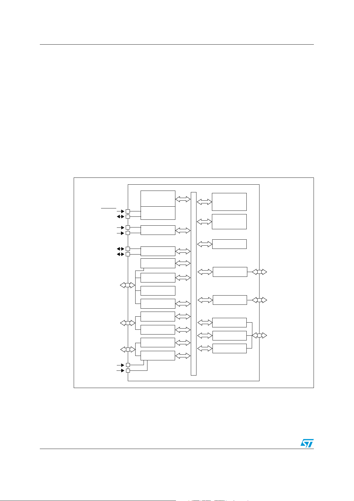
Description ST72324B-Auto
8-bit CORE
ALU
ADDRESS AND DATA BUS
OSC1
V
PP
CONTROL
Program
(8 - 32 Kbytes)
V
DD
RESET
PORT F
PF7:6, 4, 2:0
TIMER A
BEEP
PORT A
RAM
(384 - 1024 bytes)
PORT C
10-bit ADC
V
AREF
V
SSA
PORT B
PB4:0
PORT E
PE1:0
(2 bits)
SCI
TIMER B
PA7:3
(5 bits on J devices)
PORT D
PD5:0
SPI
PC7:0
(8 bits)
V
SS
WATCHDOG
OSC
LV D
OSC2
memory
MCC/RTC/BEEP
(4 bits on K devices)
(5 bits on J devices)
(3 bits on K devices)
(6 bits on J devices)
(2 bits on K devices)
(6 bits on J devices)
(5 bits on K devices)
1 Description
The ST72324B-Auto devices are members of the ST7 microcontroller family designed for
mid-range automotive applications running from 3.8 to 5.5V. Different package options offer
up to 32 I/O pins.
All devices are based on a common industry-standard 8-bit core, featuring an enhanced
instruction set and are available with Flash or ROM program memory. The ST7 family
architecture offers both power and flexibility to software developers, enabling the design of
highly efficient and compact application code.
The on-chip peripherals include an A/D converter, two general purpose timers, an SPI
interface and an SCI interface. For power economy, the microcontroller can switch
dynamically into, Slow, Wait, Active Halt or Halt mode when the application is in idle or
stand-by state.
Figure 1. Device block diagram
14/198 Doc ID13466 Rev 4
Typical applications include
● all types of car body applications such as window lift, DC motor control, rain sensors
● safety microcontroller in airbag and engine management applications
● auxiliary functions in car radios
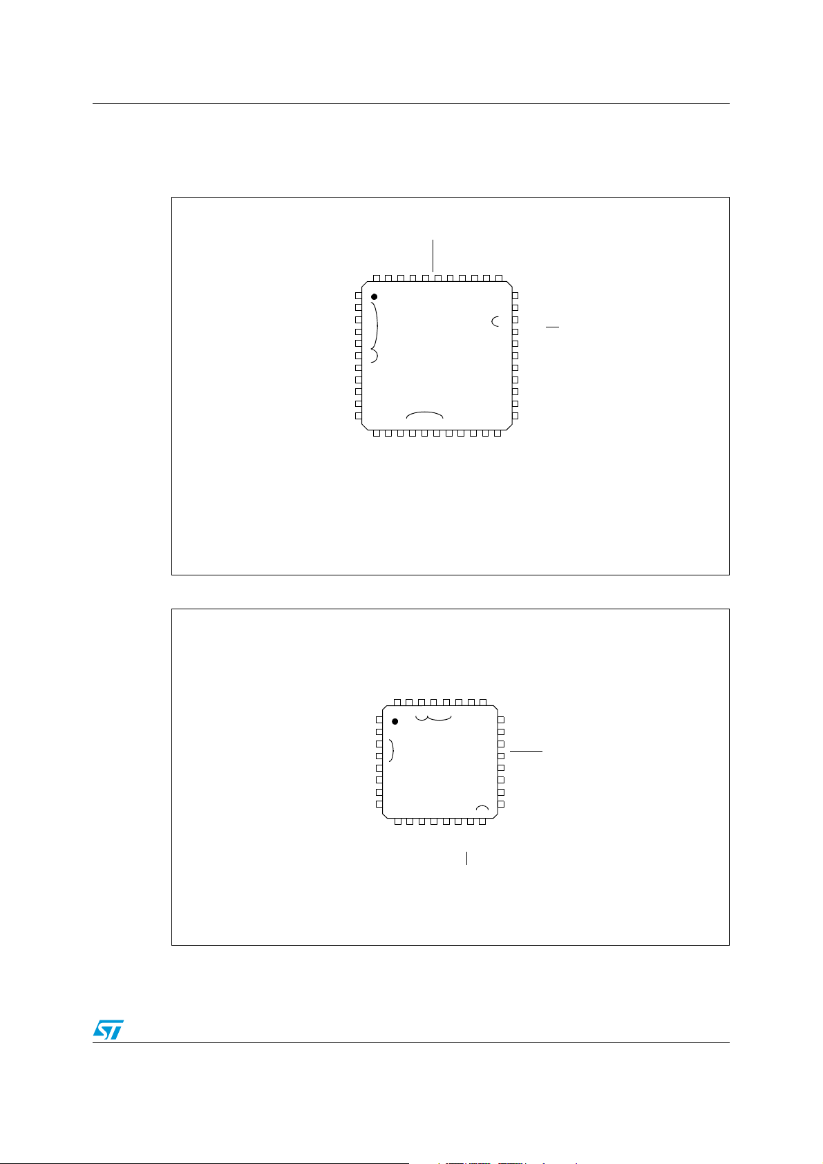
ST72324B-Auto Pin description
MCO/AIN8/PF0
BEEP/(HS) PF1
(HS) PF2
OCMP1_A/AIN10/PF4
ICAP1_A/(HS) PF6
EXTCLK_A/(HS) PF7
V
DD_0
V
SS_0
AIN5/PD5
V
AREF
V
SSA
44 43 42 41 40 39 38 37 36 35 34
33
32
31
30
29
28
27
26
25
24
23
12 13 14 15 16 17 18 19 20 21 22
1
2
3
4
5
6
7
8
9
10
11
ei2
ei3
ei0
ei1
PB3
(HS) PB4
AIN0/PD0
AIN1/PD1
AIN2/PD2
AIN3/PD3
AIN4/PD4
RDI / PE1
PB0
PB1
PB2
PC6/SCK/ICCCLK
PC5/MOSI/AIN14
PC4 / MISO/ICCDATA
PC3 (HS)/ICAP1_B
PC2 (HS)/ICAP2_B
PC1/OCMP1_B/AIN13
PC0/OCMP2_B/AIN12
V
SS_1
V
DD_1
PA3 ( HS)
PC7/SS
/AIN15
V
SS
_
2
RESET
V
PP
/ICCSEL
PA7 ( HS)
PA6 ( HS)
PA5 ( HS)
PA4 ( HS)
PE0/TDO
V
DD
_
2
OSC1
OSC2
eix associated external interrupt vector
(HS) 20mA high sink capability
ICCDATA/MISO/PC4
AIN14/MOSI/PC5
ICCCLK/SCK/PC6
AIN15/SS
/PC7
(HS) PA3
AIN13/OCMP1_B/PC1
ICAP2_B/(HS) PC2
ICAP1_B/(HS) PC3
32 31 30 29 28 27 26 25
24
23
22
21
20
19
18
17
9 10111213141516
1
2
3
4
5
6
7
8
ei1
ei3
ei0
OCMP1_A/AIN10/PF4
ICAP1_A/(HS) PF6
EXTCLK_A/(HS) PF7
AIN12/OCMP2_B/PC0
V
AREF
V
SSA
MCO/AIN8/PF0
BEEP/(HS) PF1
V
PP
/ICCSEL
PA7 ( HS)
PA6 ( HS)
PA4 ( HS)
OSC1
OSC2
V
SS_2
RESET
PB0
PE1/RDI
PE0/TDO
V
DD
_
2
PD1/AIN1
PD0/AIN0
PB4 (HS)
PB3
ei2
eix associated external interrupt vector
(HS) 20mA high sink capability
2 Pin description
Figure 2. 44-pin LQFP package pinout
Figure 3. 32-pin LQFP package pinout
See Section 12: Electrical characteristics on page 145 for external pin connection
guidelines.
Doc ID13466 Rev 4 15/198
Pin description ST72324B-Auto
Refer to Section 9: I/O ports on page 58 for more details on the software configuration of the
I/O ports.
The reset configuration of each pin is shown in bold. This configuration is valid as long as
the device is in reset state.
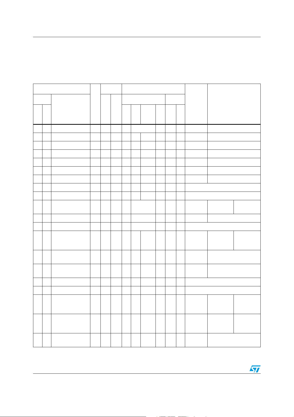
Table 2. Device pin description
No.
LQFP44
Pin
Name
LQFP32
Level Port
Type
Input
Output
float
Input Output
int
wpu
ana
OD
function
(after
reset)
PP
Main
6 30 PB4 (HS) I/O CTHS X ei3 X X Port B4
7 31 PD0/AIN0 I/O C
8 32 PD1/AIN1 I/O C
9-PD2/AIN2 I/OC
10 - PD3/AIN3 I/O C
11 - PD4/AIN4 I/O C
12 - PD5/AIN5 I/O C
13 1 V
14 2 V
AREF
SSA
(1)
(1)
15 3 PF0/MCO/AIN8 I/O C
16 4 PF1 (HS)/BEEP I/O C
17 - PF2 (HS) I/O C
18 5
PF4/OCMP1_A
/AIN10
T
T
T
T
T
T
S Analog reference voltage for ADC
S Analog ground voltage
T
T
T
I/O C
T
X X X X X Port D0 ADC analog input 0
X X X X X Port D1 ADC analog input 1
X X X X X Port D2 ADC analog input 2
X X X X X Port D3 ADC analog input 3
X X X X X Port D4 ADC analog input 4
X X X X X Port D5 ADC analog input 5
X ei1 X X X Port F0
HS X ei1 X X Port F1 Beep signal output
HS X ei1 X X Port F2
X XXXXPort F4
Alternate function
Main clock
out (f
CPU
Timer A
output
compare 1
ADC analog
)
input 8
ADC analog
Input 10
19 6
20 7
21 - V
22 - V
23 8
24 9
25 10
PF6
(HS)/ICAP1_A
PF7
(HS)/EXTCLK_A
(1)
DD_0
(1)
SS_0
PC0/OCMP2_B
/AIN12
PC1/OCMP1_B
/AIN13
PC2
(HS)/ICAP2_B
I/O C
I/O C
S Digital main supply voltage
S Digital ground voltage
I/O C
I/O C
I/O C
HS X X X X Port F6 Timer A input capture 1
T
HS X XXXPort F7
T
T
T
T
X XXXXPort C0
X XXXXPort C1
HS X X X X Port C2 Timer B input capture 2
16/198 Doc ID13466 Rev 4
Timer A external clock
source
Timer B
output
compare 2
Timer B
output
compare 1
ADC analog
input 12
ADC analog
input 13
ST72324B-Auto Pin description
Table 2. Device pin description (continued)
No.
LQFP44
26 11
27 12
28 13
29 14
Pin
Name
LQFP32
PC3
(HS)/ICAP1_B
PC4/MISO/ICCD
ATA
PC5/MOSI
/AIN14
PC6/SCK
/ICCCLK
Level Port
Type
Input
Output
I/O C
I/O C
I/O C
I/O C
HS X X X X Port C3 Timer B input capture 1
T
T
T
T
X XXXPort C4
X XXXXPort C5
X XXXPort C6
Input Output
int
wpu
float
ana
OD
function
(after
reset)
PP
Main
SPI master
in/slave out
data
SPI master
out/slave in
data
SPI serial
clock
SPI slave
30 15 PC7/SS
/AIN15 I/O C
T
X XXXXPort C7
select
(active low)
31 16 PA3 (HS) I/O C
32 - V
33 - V
DD_1
SS_1
(1)
(1)
S Digital main supply voltage
S Digital ground voltage
34 17 PA4 (HS) I/O C
35 - PA5 (HS) I/O C
36 18 PA6 (HS) I/O C
37 19 PA7 (HS) I/O CTHS X TPort A7
HS X ei0 X X Port A3
T
HS X XXXPort A4
T
HS X XXXPort A5
T
HS X TPort A6
T
(2)
(2)
Must be tied low. In the Flash
programming mode, this pin acts as
38 20 V
/ICCSEL I
PP
the programming voltage input V
See Section 12.10.2 for more details.
High voltage must not be applied to
ROM devices.
39 21 RESET
40 22 V
SS_2
41 23 OSC2
42 24 OSC1
43 25 V
DD_2
(1)
(3)
(3)
(1)
I/O C
S Digital ground voltage
O Resonator oscillator inverter output
I
S Digital main supply voltage
44 26 PE0/TDO I/O C
127PE1/RDI I/OC
T
T
T
X X X X Port E0 SCI transmit data out
X X X X Port E1 SCI receive data in
Top priority non-maskable interrupt
External clock input or resonator
oscillator inverter input
Alternate function
ICC data
input
ADC analog
input 14
ICC clock
output
ADC analog
input 15
PP
.
Doc ID13466 Rev 4 17/198
Pin description ST72324B-Auto
Table 2. Device pin description (continued)
No.
LQFP44
Pin
Name
LQFP32
Level Port
Type
Input
Output
float
Input Output
int
wpu
ana
OD
function
(after
reset)
PP
Main
Alternate function
Caution: Negative
current injection not
228PB0 I/OC
3-PB1 I/OC
4-PB2 I/OC
529PB3 I/OC
1. It is mandatory to connect all available VDD and V
2. On the chip, each I/O port has eight pads. Pads that are not bonded to external pins are in input pull-up configuration after
reset. The configuration of these pads must be kept at reset state to avoid added current consumption..
3. OSC1 and OSC2 pins connect a crystal/ceramic resonator, or an external source to the on-chip oscillator; see Section 1:
Description and Section 12.6: Clock and timing characteristics or more details.
4. For details refer to Section 12.9.1 on page 162
T
T
T
T
X ei2 X X Port B0
X ei2 X X Port B1
X ei2 X X Port B2
X ei2 X X Port B3
pins to the supply voltage and all VSS and V
REF
allowed on this pin on
8/16 Kbyte Flash
devices.
(4)
pins to ground.
SSA
Legend / Abbreviations for Tabl e 2:
Type:I = input, O = output, S = supply
Input level: A = Dedicated analog input
In/Output level: C = CMOS 0.3V
DD
/0.7
DD
CT = CMOS 0.3VDD/0.7DD with input trigger
Output level: HS = 20mA high sink (on N-buffer only)
Port and control configuration:
Input:float = floating, wpu = weak pull-up, int = interrupt
Output:OD = open drain
(b)
, PP = push-pull
(a)
, ana = analog ports
a. In the interrupt input column, “eiX” defines the associated external interrupt vector. If the weak pull-up column
(wpu) is merged with the interrupt column (int), then the I/O configuration is pull-up interrupt input, else the
configuration is floating interrupt input.
b. In the open drain output column, ‘T’ defines a true open drain I/O (P-Buffer and protection diode to V
implemented). See Section 9: I/O ports and Section 12.9: I/O port pin characteristics for more details.
18/198 Doc ID13466 Rev 4
are not
DD
ST72324B-Auto Register and memory map
0000h
RAM
Program memory
(32, 16 or 8 Kbytes)
Interrupt and reset vectors
HW registers
0080h
007Fh
7FFFh
(see Tabl e 3)
8000h
FFDFh
FFE0h
FFFFh
(see Table 25)
0480h
Reserved
047Fh
Short addressing
RAM (zero page)
256 bytes stack
16-bit addressing
RAM
0100h
01FFh
027Fh
0080h
0200h
00FFh
32 Kbytes
8000h
FFFFh
or 047Fh
16 Kbytes
C000h
(1024, 512 or 384 bytes)
8 Kbytes
E000h
3 Register and memory map
As shown in Figure 4 the MCU is capable of addressing 64 Kbytes of memories and I/O
registers.
The available memory locations consist of 128 bytes of register locations, up to 1024 bytes
of RAM and up to 32 Kbytes of user program memory. The RAM space includes up to 256
bytes for the stack from 0100h to 01FFh.
The highest address bytes contain the user reset and interrupt vectors.
Caution: Never access memory locations marked as ‘Reserved’. Accessing a reserved area can
have unpredictable effects on the device.
Figure 4. Memory map
Table 3. Hardware register map
Address Block Register label Register name
0000h
0001h
0002h
0003h
0004h
0005h
0006h
0007h
0008h
0009h
000Ah
000Bh
000Ch
000Dh
000Eh
Por t A
Por t B
Por t C
Por t D
Por t E
(2)
(1)
(1)
(1)
PA DR
PADDR
PA OR
PBDR
PBDDR
PBOR
PCDR
PCDDR
PCOR
PDADR
PDDDR
PDOR
PEDR
PEDDR
PEOR
Port A data register
Port A data direction register
Port A option register
Port B data register
Port B data direction register
Port B option register
Port C data register
Port C data direction register
Port C option register
Port D data register
Port D data direction register
Port D option register
Port E data register
Port E data direction register
Port E option register
Reset
status
00h
00h
00h
00h
00h
00h
00h
00h
00h
00h
00h
00h
00h
00h
00h
(3)
(2)
(2)
(2)
(2)
(1)
Remarks
R/W
R/W
R/W
R/W
R/W
R/W
R/W
R/W
R/W
R/W
R/W
R/W
R/W
R/W
R/W
(1)
(1)
(1)
Doc ID13466 Rev 4 19/198
Register and memory map ST72324B-Auto
Table 3. Hardware register map (continued)
Address Block Register label Register name
000Fh
0010h
0011h
0012h to
0020h
0021h
0022h
0023h
0024h
0025h
0026h
0027h
Por t F
SPI
ITC
(1)
PFDR
PFDDR
PFOR
SPIDR
SPICR
SPICSR
ISPR0
ISPR1
ISPR2
ISPR3
Port F data register
Port F data direction register
Port F option register
Reserved area (15 bytes)
SPI data I/O register
SPI control register
SPI control/status register
Interrupt software priority register 0
Interrupt software priority register 1
Interrupt software priority register 2
Interrupt software priority register 3
Reset
status
00h
00h
00h
xxh
0xh
00h
FFh
FFh
FFh
FFh
(1)
(2)
0028h EICR External interrupt control register 00h R/W
0029h Flash FCSR Flash control/status register 00h R/W
002Ah Watchdog WDGCR Watchdog control register 7Fh R/W
002Bh SI SICSR System integrity control/status register 000x 000xb R/W
002Ch
002Dh
002Eh to
0030h
MCC
MCCSR
MCCBCR
Main clock control/status register
Main clock controller: beep control register
Reserved area (3 bytes)
00h
00h
Remarks
R/W
R/W
R/W
R/W
R/W
R/W
R/W
R/W
R/W
R/W
R/W
R/W
(1)
0031h
0032h
0033h
0034h
0035h
0036h
0037h
0038h
0039h
003Ah
003Bh
003Ch
003Dh
003Eh
003Fh
Timer A
TACR2
TACR1
TACS R
TA IC 1 H R
TA IC 1 L R
TAOC 1 H R
TAOC1LR
TACHR
TACL R
TAACHR
TA AC L R
TA IC 2 H R
TA IC 2 L R
TAOC 2 H R
TAOC2LR
Timer A control register 2
Timer A control register 1
Timer A control/status register
Timer A input capture 1 high register
Timer A input capture 1 low register
Timer A output compare 1 high register
Timer A output compare 1 low register
Timer A counter high register
Timer A counter low register
Timer A alternate counter high register
Timer A alternate counter low register
Timer A input capture 2 high register
Timer A input capture 2 low register
Timer A output compare 2 high register
Timer A output compare 2 low register
0040h Reserved area (1 byte)
00h
00h
xxxx x0xxb
xxh
xxh
80h
00h
FFh
FCh
FFh
FCh
xxh
xxh
80h
00h
R/W
R/W
R/W
Read only
Read only
R/W
R/W
Read only
Read only
Read only
Read only
Read only
Read only
R/W
R/W
20/198 Doc ID13466 Rev 4
ST72324B-Auto Register and memory map
Table 3. Hardware register map (continued)
Address Block Register label Register name
0041h
0042h
0043h
0044h
0045h
0046h
0047h
0048h
0049h
004Ah
004Bh
004Ch
004Dh
004Eh
004Fh
0050h
0051h
0052h
0053h
0054h
0055h
0056h
0057h
Timer B
SCI
TBCR2
TBCR1
TBCSR
TBIC1HR
TBIC1LR
TBOC1HR
TBOC1LR
TBCHR
TBCLR
TBACHR
TBACLR
TBIC2HR
TBIC2LR
TBOC2HR
TBOC2LR
SCISR
SCIDR
SCIBRR
SCICR1
SCICR2
SCIERPR
SCIETPR
Timer B control register 2
Timer B control register 1
Timer B control/status register
Timer B input capture 1 high register
Timer B input capture 1 low register
Timer B output compare 1 high register
Timer B output compare 1 low register
Timer B counter high register
Timer B counter low register
Timer B alternate counter high register
Timer B alternate counter low register
Timer B input capture 2 high register
Timer B input capture 2 low register
Timer B output compare 2 high register
Timer B output compare 2 low register
SCI status register
SCI data register
SCI baud rate register
SCI control register 1
SCI control register 2
SCI extended receive prescaler register
Reserved area
SCI extended transmit prescaler register
Reset
(1)
status
00h
00h
xxxx x0xxb
xxh
xxh
80h
00h
FFh
FCh
FFh
FCh
xxh
xxh
80h
00h
C0h
xxh
00h
x000 0000b
00h
00h
---
00h
Remarks
R/W
R/W
R/W
Read only
Read only
R/W
R/W
Read only
Read only
Read only
Read only
Read only
Read only
R/W
R/W
Read only
R/W
R/W
R/W
R/W
R/W
R/W
(1)
0058h to
006Fh
0070h
0071h
0072h
ADC
ADCCSR
ADCDRH
ADCDRL
Control/status register
Data high register
Data low register
0073h
007Fh
1. Legend: x = undefined, R/W = read/write.
2. The bits associated with unavailable pins must always keep their reset value.
3. The contents of the I/O port DR registers are readable only in output configuration. In input configuration, the values of the
I/O pins are returned instead of the DR register contents.
Reserved area (24 bytes)
Reserved area (13 bytes)
00h
00h
00h
R/W
Read only
Read only
Doc ID13466 Rev 4 21/198

Flash program memory ST72324B-Auto
4 Flash program memory
4.1 Introduction
The ST7 dual voltage High Density Flash (HDFlash) is a non-volatile memory that can be
electrically erased as a single block or by individual sectors and programmed on a byte-bybyte basis using an external V
The HDFlash devices can be programmed and erased off-board (plugged in a programming
tool) or on-board using ICP (in-circuit programming) or IAP (in-application programming).
The array matrix organization allows each sector to be erased and reprogrammed without
affecting other sectors.
4.2 Main features
● 3 Flash programming modes:
– Insertion in a programming tool. In this mode, all sectors including option bytes
can be programmed or erased.
– ICP (in-circuit programming). In this mode, all sectors including option bytes can
be programmed or erased without removing the device from the application board.
– IAP (in-application programming). In this mode, all sectors, except Sector 0, can
be programmed or erased without removing the device from the application board
and while the application is running.
● ICT (in-circuit testing) for downloading and executing user application test patterns in
RAM
● Readout protection
● Register Access Security System (RASS) to prevent accidental programming or
erasing
supply.
PP
4.3 Structure
The Flash memory is organized in sectors and can be used for both code and data storage.
Depending on the overall Flash memory size in the microcontroller device, there are up to
three user sectors (see
unnecessary erasing of the whole Flash memory when only a partial erasing is required.
The first two sectors have a fixed size of 4 Kbytes (see Figure 5). They are mapped in the
upper part of the ST7 addressing space so the reset and interrupt vectors are located in
Sector 0 (F000h-FFFFh).
Table 4. Sectors available in Flash devices
Flash size (bytes) Available sectors
22/198 Doc ID13466 Rev 4
Ta ble 4). Each of these sectors can be erased independently to avoid
4K Sector 0
8K Sectors 0, 1
>8K Sectors 0, 1, 2
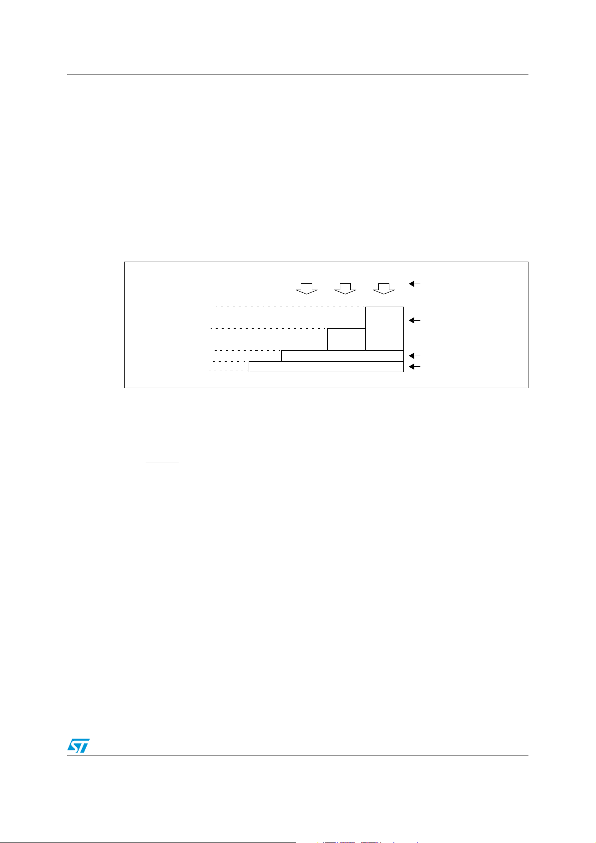
ST72324B-Auto Flash program memory
4Kbytes
4Kbytes
Sector 1
Sector 0
Sector 2
8K 16K
32K
Flash
FFFFh
EFFFh
DFFFh
7FFFh
24 Kbytes
memory size
8Kbytes
BFFFh
4.3.1 Readout protection
Readout protection, when selected, provides a protection against program memory content
extraction and against write access to Flash memory. Even if no protection can be
considered as totally unbreakable, the feature provides a very high level of protection for a
general purpose microcontroller.
In Flash devices, this protection is removed by reprogramming the option. In this case, the
entire program memory is first automatically erased.
Readout protection selection depends on the device type:
● In Flash devices it is enabled and removed through the FMP_R bit in the option byte.
● In ROM devices it is enabled by mask option specified in the option list.
Figure 5. Memory map and sector address
4.4 ICC interface
ICC needs a minimum of 4 and up to 6 pins to be connected to the programming tool (see
Figure 6). These pins are:
● RESET: device reset
● V
● ICCCLK: ICC output serial clock pin
● ICCDATA: ICC input/output serial data pin
● ICCSEL/V
● OSC1 (or OSCIN): main clock input for external source (optional)
● V
: device power supply ground
SS
: programming voltage
PP
: application board power supply (optional, see Figure 6, Note 3).
DD
Doc ID13466 Rev 4 23/198
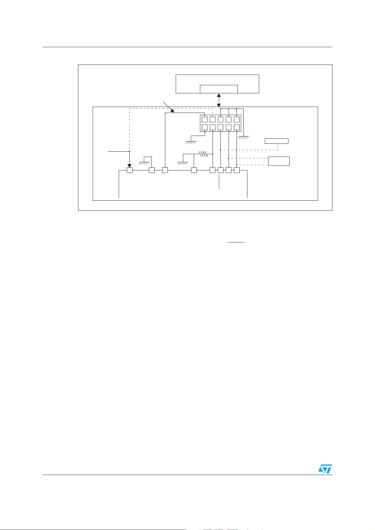
Flash program memory ST72324B-Auto
ICC connector
ICCDATA
ICCCLK
RESET
V
DD
HE10 connector type
Application
power supply
1
246810
975 3
Programming tool
ICC connector
Application board
ICC cable
(See note 3)
10k
V
SS
ICCSEL/VPP
ST7
OSC1
OSC2
Mandatory for
See note 1
See note 2
Application
reset source
Application
I/O
(see note 4)
8/16 Kbyte Flash devices
Figure 6. Typical ICC interface
1. If the ICCCLK or ICCDATA pins are only used as outputs in the application, no signal isolation is
necessary. As soon as the programming tool is plugged to the board, even if an ICC session is not in
progress, the ICCCLK and ICCDATA pins are not available for the application. If they are used as inputs by
the application, isolation such as a serial resistor has to be implemented in case another device forces the
signal. Refer to the Programming Tool documentation for recommended resistor values.
2. During the ICC session, the programming tool must control the RESET
between the programming tool and the application reset circuit if it drives more than 5mA at high level
(PUSH-pull output or pull-up resistor <1K). A schottky diode can be used to isolate the application reset
circuit in this case. When using a classical RC network with R>1K or a reset management IC with open
drain output and pull-up resistor >1K, no additional components are needed. In all cases the user must
ensure that no external reset is generated by the application during the ICC session.
3. The use of Pin 7 of the ICC connector depends on the programming tool architecture. This pin must be
connected when using most ST programming tools (it is used to monitor the application power supply).
Please refer to the programming tool manual.
4. Pin 9 has to be connected to the OSC1 (OSCIN) pin of the ST7 when the clock is not available in the
application or if the selected clock option is not programmed in the option byte. ST7 devices with multioscillator capability need to have OSC2 grounded in this case.
pin. This can lead to conflicts
Caution: External clock ICC entry mode is mandatory in ST72F324B 8/16 Kbyte Flash devices. In
this case pin 9 must be connected to the OSC1 (OSCIN) pin of the ST7 and OSC2 must be
grounded. 32 Kbyte Flash devices may use external clock or application clock ICC entry
mode.
4.5 ICP (in-circuit programming)
To perform ICP the microcontroller must be switched to ICC (in-circuit communication) mode
by an external controller or programming tool.
Depending on the ICP code downloaded in RAM, Flash memory programming can be fully
24/198 Doc ID13466 Rev 4
customized (number of bytes to program, program locations, or selection serial
communication interface for downloading).
When using an STMicroelectronics or third-party programming tool that supports ICP and
the specific microcontroller device, the user needs only to implement the ICP hardware
interface on the application board (see
to the device pinout description.
Figure 6). For more details on the pin locations, refer
ST72324B-Auto Flash program memory
4.6 IAP (in-application programming)
This mode uses a BootLoader program previously stored in Sector 0 by the user (in ICP
mode or by plugging the device in a programming tool).
This mode is fully controlled by user software. This allows it to be adapted to the user
application, (such as user-defined strategy for entering programming mode, choice of
communications protocol used to fetch the data to be stored). For example, it is possible to
download code from the SPI, SCI, USB or CAN interface and program it in the Flash. IAP
mode can be used to program any of the Flash sectors except Sector 0, which is write/erase
protected to allow recovery in case errors occur during the programming operation.
4.7 Related documentation
For details on Flash programming and ICC protocol, refer to the ST7 Flash Programming
Reference Manual and to the ST7 ICC Protocol Reference Manual
4.7.1 Flash Control/Status Register (FCSR)
This register is reserved for use by programming tool software. It controls the Flash
programming and erasing operations.
FCSR Reset value:0000 0000 (00h)
76543210
.
00000000
R/W R/W R/W R/W R/W R/W R/W R/W
Table 5. Flash control/status register address and reset value
Address (Hex) Register label 7 6 5 4 3 2 1 0
0029h FCSR reset value 0 0 0 0 0 0 0 0
Doc ID13466 Rev 4 25/198
Central processing unit (CPU) ST72324B-Auto
Accumulator
X index register
Y index register
Stack pointer
Condition code register
Program counter
70
1C1I1HI0NZ
Reset value = reset vector @ FFFEh-FFFFh
70
70
70
0
7
15 8
PCH
PCL
15
87 0
Reset value = stack higher address
Reset value = 1 X11X1XX
Reset value = XXh
Reset value = XXh
Reset value = XXh
X = undefined value
5 Central processing unit (CPU)
5.1 Introduction
This CPU has a full 8-bit architecture and contains six internal registers allowing efficient 8bit data manipulation.
5.2 Main features
● Enable executing 63 basic instructions
● Fast 8-bit by 8-bit multiply
● 17 main addressing modes (with indirect addressing mode)
● Two 8-bit index registers
● 16-bit stack pointer
● Low power Halt and Wait modes
● Priority maskable hardware interrupts
● Non-maskable software/hardware interrupts
5.3 CPU registers
The six CPU registers shown in Figure 7 are not present in the memory mapping and are
accessed by specific instructions.
Figure 7. CPU registers
26/198 Doc ID13466 Rev 4

ST72324B-Auto Central processing unit (CPU)
5.3.1 Accumulator (A)
The Accumulator is an 8-bit general purpose register used to hold operands and the results
of the arithmetic and logic calculations and to manipulate data.
5.3.2 Index registers (X and Y)
These 8-bit registers are used to create effective addresses or as temporary storage areas
for data manipulation. (The Cross-Assembler generates a precede instruction (PRE) to
indicate that the following instruction refers to the Y register.)
The Y register is not affected by the interrupt automatic procedures.
5.3.3 Program counter (PC)
The program counter is a 16-bit register containing the address of the next instruction to be
executed by the CPU. It is made of two 8-bit registers PCL (Program Counter Low which is
the LSB) and PCH (Program Counter High which is the MSB).
5.3.4 Condition Code register (CC)
The 8-bit Condition Code register contains the interrupt masks and four flags representative
of the result of the instruction just executed. This register can also be handled by the PUSH
and POP instructions. These bits can be individually tested and/or controlled by specific
instructions.
CC Reset value: 111x1xxx
76543210
11I1HI0NZC
R/W R/W R/W R/W R/W R/W R/W R/W
Table 6. Arithmetic management bits
BIt Name Function
Half carry
This bit is set by hardware when a carry occurs between bits 3 and 4 of the ALU
during an ADD or ADC instructions. It is reset by hardware during the same
4H
2N
instructions.
0: No half carry has occurred.
1: A half carry has occurred.
This bit is tested using the JRH or JRNH instruction. The H bit is useful in BCD
arithmetic subroutines.
Negative
This bit is set and cleared by hardware. It is representative of the result sign of the last
arithmetic, logical or data manipulation. It is a copy of the result 7th bit.
0: The result of the last operation is positive or null.
1: The result of the last operation is negative (that is, the most significant bit is a logic
1.
This bit is accessed by the JRMI and JRPL instructions.
Doc ID13466 Rev 4 27/198
Central processing unit (CPU) ST72324B-Auto
Table 6. Arithmetic management bits (continued)
BIt Name Function
Zero (Arithmetic Management bit)
This bit is set and cleared by hardware. This bit indicates that the result of the last
1Z
0C
Table 7. Software interrupt bits
BIt Name Function
5I1
3I0
arithmetic, logical or data manipulation is zero.
0: The result of the last operation is different from zero.
1: The result of the last operation is zero.
This bit is accessed by the JREQ and JRNE test instructions.
Carry/borrow
This bit is set and cleared by hardware and software. It indicates an overflow or an
underflow has occurred during the last arithmetic operation.
0: No overflow or underflow has occurred.
1: An overflow or underflow has occurred.
This bit is driven by the SCF and RCF instructions and tested by the JRC and JRNC
instructions. It is also affected by the ‘bit test and branch’, shift and rotate instructions.
Software Interrupt Priority 1
The combination of the I1 and I0 bits determines the current interrupt software priority
(see Ta b le 8).
Software Interrupt Priority 0
The combination of the I1 and I0 bits determines the current interrupt software priority
(see Ta b le 8).
Table 8. Interrupt software priority selection
Interrupt software priority Level I1 I0
Level 0 (main)
Low
10
Level 1 01
Level 2 00
Level 3 (= interrupt disable) 1 1
High
These two bits are set/cleared by hardware when entering in interrupt. The loaded value is
given by the corresponding bits in the interrupt software priority registers (ISPRx). They can
be also set/cleared by software with the RIM, SIM, IRET, HALT, WFI and PUSH/POP
instructions.
See Section 7: Interrupts on page 41 for more details.
28/198 Doc ID13466 Rev 4

ST72324B-Auto Central processing unit (CPU)
5.3.5 Stack Pointer register (SP)
SP Reset value: 01 FFh
1514131211109876543210
00000001SP7SP6SP5SP4SP3SP2SP1SP0
R/W R/W R/W R/W R/W R/W R/W R/W R/W R/W R/W R/W R/W R/W R/W R/W
The Stack Pointer is a 16-bit register which is always pointing to the next free location in the
stack. It is then decremented after data has been pushed onto the stack and incremented
before data is popped from the stack (see
Since the stack is 256 bytes deep, the 8 most significant bits are forced by hardware.
Following an MCU reset, or after a Reset Stack Pointer instruction (RSP), the Stack Pointer
contains its reset value (the SP7 to SP0 bits are set) which is the stack higher address.
The least significant byte of the Stack Pointer (called S) can be directly accessed by an LD
instruction.
Note: When the lower limit is exceeded, the Stack Pointer wraps around to the stack upper limit,
without indicating the stack overflow. The previously stored information is then overwritten
and therefore lost. The stack also wraps in case of an underflow.
Figure 8).
The stack is used to save the return address during a subroutine call and the CPU context
during an interrupt. The user may also directly manipulate the stack by means of the PUSH
and POP instructions. In the case of an interrupt, the PCL is stored at the first location
pointed to by the SP. Then the other registers are stored in the next locations as shown in
Figure 8.
● When an interrupt is received, the SP is decremented and the context is pushed on the
stack.
● On return from interrupt, the SP is incremented and the context is popped from the
stack.
A subroutine call occupies two locations and an interrupt five locations in the stack area.
Doc ID13466 Rev 4 29/198
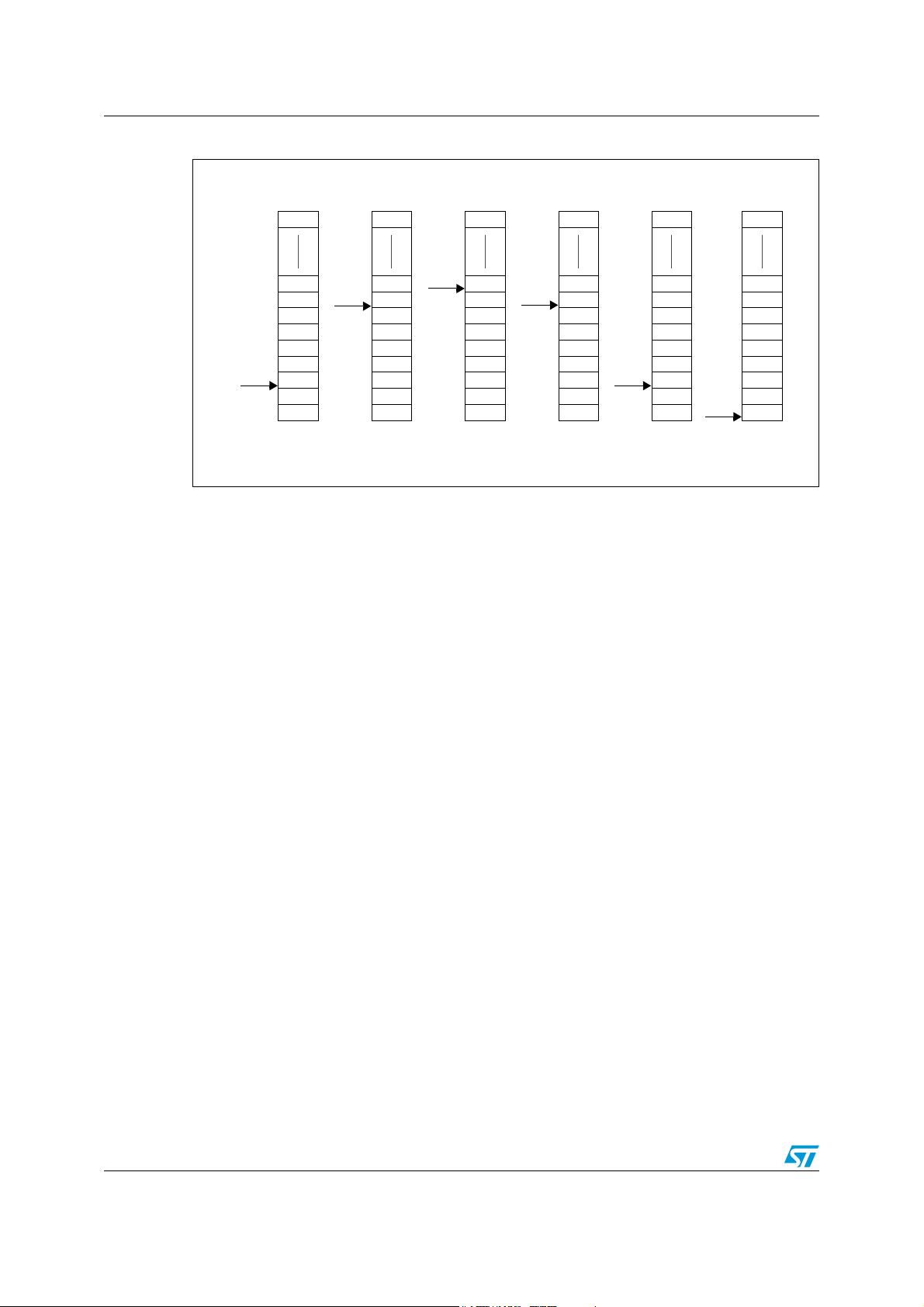
Central processing unit (CPU) ST72324B-Auto
PCH
PCL
SP
PCH
PCL
SP
PCL
PCH
X
A
CC
PCH
PCL
SP
PCL
PCH
X
A
CC
PCH
PCL
SP
PCL
PCH
X
A
CC
PCH
PCL
SP
SP
Y
Call
subroutine
Interrupt
event
Push Y Pop Y IRET
RET
or RSP
@ 01FFh
@ 0100h
Stack Higher Address = 01FFh
Stack Lower Address =
0100h
Figure 8. Stack manipulation example
30/198 Doc ID13466 Rev 4
Loading...