


 Loading...
TDA7440
TONE CONTROL DIGITALLY CONTROLLED AUDIO PROCESSOR
1 FEATURES
INPUT MULTIPLEXER
–4 STEREO INPUTS
–SELECTABLE INPUT GAIN FOR OPTIMAL ADAPTATION TO DIFFERENT SOURCES
ONE STEREO OUTPUT
TREBLE AND BASS CONTROL IN 2.0dB STEPS
VOLUME CONTROL IN 1.0dB STEPS
TWO SPEAKER ATTENUATORS:
–TWO INDEPENDENT SPEAKER CONTROL IN 1.0dB STEPS FOR BALANCE FACILITY
–INDEPENDENT MUTE FUNCTION
ALL FUNCTION ARE PROGRAMMABLE VIA SERIAL BUS
2 DESCRIPTION
The TDA7440D is a volume tone (bass and treble) balance (Left/Right) processor for quality audio applications in Hi-Fi systems.
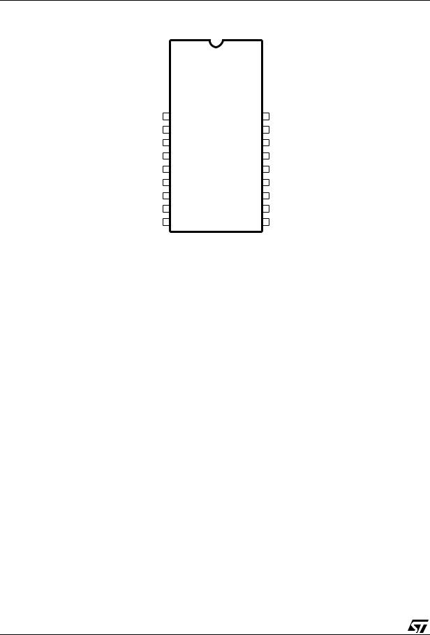
Figure 1. Package
SO-28 |
|
|
|
|
|
Table 1. Order Codes |
|
|
|
|
|
Order code |
|
Package |
|
|
|
TDA7440D |
|
SO-28 |
|
|
|
TDA7440D013TR |
|
Tape & Reel |
|
|
|
Selectable input gain is provided. Control of all the functions is accomplished by serial bus.
The AC signal setting is obtained by resistor networks and switches combined with operational amplifiers.
Thanks to the used BIPOLAR/CMOS Technology, Low Distortion, Low Noise and DC stepping are obtained
Figure 2. Block Diagram
|
|
|
MUXOUTL |
INL |
TREBLE(L) |
BIN(L) |
BOUT(L) |
|
|
4 |
|
|
8 |
9 |
18 |
14 |
15 |
|
|
L-IN1 |
|
|
|
|
|
|
|
|
|
|
100K |
|
|
|
|
RB |
|
|
|
5 |
|
|
|
|
|
|
|
|
|
L-IN2 |
|
|
|
|
|
|
|
|
|
|
100K |
|
|
|
|
|
|
|
|
6 |
|
G |
VOLUME |
TREBLE |
BASS |
SPKR ATT |
27 |
||
|
|
LEFT |
LOUT |
||||||
L-IN3 |
|
|
|
|
|
|
|
|
|
|
|
|
|
|
|
|
|
|
|
|
100K |
|
|
|
|
|
|
|
|
7 |
|
|
|
|
|
|
|
|
|
L-IN4 |
|
|
|
|
|
|
|
|
|
|
100K |
|
|
|
|
|
|
|
21 |
|
|
0/30dB |
|
|
|
|
|
|
|
|
|
|
|
I2CBUS DECODER + LATCHES |
|
|
SCL |
||
3 |
|
2dB STEP |
|
|
|
|
22 |
||
|
|
|
|
|
|
|
SDA |
||
|
|
|
|
|
|
|
|
||
R-IN1 |
|
|
|
|
|
|
|
|
20 |
|
100K |
|
|
|
|
|
|
|
DIG_GND |
|
|
|
|
|
|
|
|
|
|
2 |
|
|
|
|
|
|
|
|
|
R-IN2 |
|
|
|
|
|
|
|
|
|
|
100K |
G |
VOLUME |
TREBLE |
BASS |
SPKR ATT |
26 |
||
|
|
|
RIGHT |
ROUT |
|||||
|
|
|
|
|
|
|
|
|
|
1 |
|
|
|
|
|
|
|
|
|
R-IN3 |
|
|
|
|
|
|
|
VREF |
|
|
100K |
|
|
|
|
|
|
|
|
28 |
|
|
|
|
|
|
|
|
24 |
|
|
|
|
|
|
|
SUPPLY |
VS |
|
R-IN4 |
|
INPUT MULTIPLEXER |
|
|
|
|
|
25 |
|
|
100K |
|
|
|
RB |
|
|
AGND |
|
|
+ GAIN |
|
|
|
|
|
|
||
|
|
|
|
|
|
|
|
|
|
|
|
|
10 |
11 |
19 |
12 |
13 |
23 |
|
|
|
|
MUXOUTR |
INR |
TREBLE(R) |
BIN(R) |
BOUT(R) |
CREF |
D98AU883 |
REV. 4
April 2010 |
1/17 |
TDA7440
Figure 3. Pin Connection (Top view)
R_IN3 |
|
|
28 |
|
|
1 |
|
R_IN4 |
|||
R_IN2 |
|
2 |
27 |
|
LOUT |
|
|
||||
R_IN1 |
|
3 |
26 |
|
ROUT |
|
|
||||
L_IN1 |
|
4 |
25 |
|
AGND |
|
|
||||
L_IN2 |
|
5 |
24 |
|
VS |
|
|
||||
|
|
||||
L_IN3 |
6 |
23 |
|
CREF |
|
L_IN4 |
7 |
22 |
|
SDA |
|
MUXOUTL |
8 |
21 |
|
SCL |
|
IN(L) |
9 |
20 |
|
DIG-GND |
|
MUXOUT(R) |
10 |
19 |
|
TREBLE(R) |
|
IN(R) |
11 |
18 |
|
TREBLE(L) |
|
BIN(R) |
12 |
17 |
|
N.C. |
|
BOUT(R) |
13 |
16 |
|
N.C. |
|
BIN(L) |
14 |
15 |
|
BOUT(L) |
|
|
|
|
D98AU884 |
|
|
|
|
|
|
|
|
Table 2. Absolute Maximum Ratings
Symbol |
Parameter |
Value |
Unit |
|
|
|
|
VS |
Operating Supply Voltage |
10.5 |
V |
Tamb |
Operating Ambient Temperature |
0 to 70 |
°C |
Tstg |
Storage Temperature Range |
-55 to 150 |
°C |
Table 3. Thermal Data
Symbol |
Parameter |
Value |
Unit |
|
|
|
|
Rth j-pin |
Thermal Resistance Junction-pins |
85 |
°C/W |
Table 4. Quick Reference Data
Symbol |
Parameter |
Min. |
Typ. |
Max. |
Unit |
|
|
|
|
|
|
VS |
Supply Voltage |
6 |
9 |
10.2 |
V |
VCL |
Max. input signal handling |
2 |
|
|
Vrms |
THD |
Total Harmonic Distortion V = 1Vrms f = 1KHz |
0.01 |
0.1 |
% |
|
|
|
|
|
|
|
S/N |
Signal to Noise Ratio Vout = 1Vrms (mode = OFF) |
|
106 |
|
dB |
SC |
Channel Separation f = 1KHz |
|
90 |
|
dB |
|
Input Gain in (2dB step) |
0 |
|
30 |
dB |
|
|
|
|
|
|
|
Volume Control (1dB step) |
-47 |
|
0 |
dB |
|
|
|
|
|
|
|
Treble Control (2dB step) |
-14 |
|
+14 |
dB |
|
|
|
|
|
|
|
Bass Control (2dB step) |
-14 |
|
+14 |
dB |
|
|
|
|
|
|
|
Balance Control 1dB step |
-79 |
|
0 |
dB |
|
|
|
|
|
|
|
Mute Attenuation |
|
100 |
|
dB |
|
|
|
|
|
|
2/17

TDA7440
Table 5. Electrical Characteristcs
Refer to the test circuit Tamb = 25°C, VS = 9V, RL = 10KΩ, RG = 600Ω, all controls flat (G = 0dB), unless otherwise specified.
Symbol |
Parameter |
Test Condition |
Min. |
Typ. |
Max. |
Unit |
|
|
|
|
|
|
|
SUPPLY |
|
|
|
|
|
|
|
|
|
|
|
|
|
VS |
Supply Voltage |
|
6 |
9 |
10.2 |
V |
IS |
Supply Current |
|
4 |
7 |
10 |
mA |
SVR |
Ripple Rejection |
|
60 |
90 |
|
dB |
|
|
|
|
|
|
|
INPUT STAGE |
|
|
|
|
|
|
|
|
|
|
|
|
|
RIN |
Input Resistance |
|
70 |
100 |
130 |
KΩ |
VCL |
Clipping Level |
THD = 0.3% |
2 |
2.5 |
|
Vrms |
SIN |
Input Separation |
The selected input is grounded |
80 |
100 |
|
dB |
|
|
through a 2.2µ capacitor |
|
|
|
|
Ginmin |
Minimum Input Gain |
|
-1 |
0 |
1 |
dB |
Ginman |
Maximum Input Gain |
|
29 |
30 |
31 |
dB |
Gstep |
Step Resolution |
|
1.5 |
2 |
2.5 |
dB |
VOLUME CONTROL |
|
|
|
|
|
|
|
|
|
|
|
|
|
Ri |
Input Resistance |
|
20 |
33 |
50 |
KΩ |
CRANGE |
Control Range |
|
45 |
47 |
49 |
dB |
AVMAX |
Max. Attenuation |
|
45 |
47 |
49 |
dB |
ASTEP |
Step Resolution |
|
0.5 |
1 |
1.5 |
dB |
EA |
Attenuation Set Error |
AV = 0 to -24dB |
-1.0 |
0 |
1.0 |
dB |
|
|
AV = -24 to -47dB |
-1.5 |
0 |
1.5 |
dB |
ET |
Tracking Error |
AV = 0 to -24dB |
|
0 |
1 |
dB |
|
|
AV = -24 to -47dB |
|
0 |
2 |
dB |
VDC |
DC Step |
adjacent attenuation steps from |
|
0 |
3 |
mV |
|
|
0dB to AV max |
|
0.5 |
|
mV |
Amute |
Mute Attenuation |
|
80 |
100 |
|
dB |
BASS CONTROL (1) |
|
|
|
|
|
|
|
|
|
|
|
|
|
Gb |
Control Range |
Max. Boost/cut |
+12.0 |
+14.0 |
+16.0 |
dB |
|
|
|
|
|
|
|
BSTEP |
Step Resolution |
|
1 |
2 |
3 |
dB |
RB |
Internal Feedback Resistance |
|
33 |
44 |
55 |
KΩ |
TREBLE CONTROL (1) |
|
|
|
|
|
|
|
|
|
|
|
|
|
Gt |
Control Range |
Max. Boost/cut |
+13.0 |
+14.0 |
+15.0 |
dB |
|
|
|
|
|
|
|
TSTEP |
Step Resolution |
|
1 |
2 |
3 |
dB |
SPEAKER ATTENUATORS |
|
|
|
|
|
|
|
|
|
|
|
|
|
CRANGE |
Control Range |
|
70 |
76 |
82 |
dB |
SSTEP |
Step Resolution |
|
0.5 |
1 |
1.5 |
dB |
EA |
Attenuation Set Error |
AV = 0 to -20dB |
-1.5 |
0 |
1.5 |
dB |
|
|
AV = -20 to -56dB |
-2 |
0 |
2 |
dB |
VDC |
DC Step |
adjacent attenuation steps |
|
0 |
3 |
mV |
Amute |
Mute Attenuation |
|
80 |
100 |
|
dB |
NOTE1:
1)The device is functionally good at Vs = 5V. a step down, on Vs, to 4V does’t reset the device.
2)BASS and TREBLE response: The center frequency and the response quality can be chosen by the external circuitry.
3/17

TDA7440
Table 5. Electrical Characteristcs (continued)
Refer to the test circuit Tamb = 25°C, VS = 9V, RL = 10KΩ, RG = 600Ω, all controls flat (G = 0dB), unless otherwise specified.
Symbol |
Parameter |
Test Condition |
Min. |
Typ. |
Max. |
Unit |
|
|
|
|
|
|
|
AUDIO OUTPUTS |
|
|
|
|
|
|
|
|
|
|
|
|
|
VCLIP |
Clipping Level |
d = 0.3% |
2.1 |
2.6 |
|
Vrms |
RL |
Output Load Resistance |
|
2 |
|
|
KΩ |
RO |
Output Impedance |
|
10 |
30 |
50 |
Ω |
VDC |
DC Voltage Level |
|
3.5 |
3.8 |
4.1 |
V |
GENERAL |
|
|
|
|
|
|
|
|
|
|
|
|
|
ENO |
Output Noise |
All gains = 0dB; |
|
5 |
15 |
µV |
|
|
BW = 20Hz to 20KHz flat |
|
|
|
|
|
|
|
|
|
|
|
Et |
Total Tracking Error |
AV = 0 to -24dB |
|
0 |
1 |
dB |
|
|
AV = -24 to -47dB |
|
0 |
2 |
dB |
S/N |
Signal to Noise Ratio |
All gains 0dB; VO = 1Vrms |
95 |
106 |
|
dB |
SC |
Channel Separation Left/Right |
|
80 |
100 |
|
dB |
d |
Distortion |
AV = 0; VI = 1Vrms |
|
0.01 |
0.08 |
% |
BUS INPUT |
|
|
|
|
|
|
|
|
|
|
|
|
|
VIL |
Input Low Voltage |
|
|
|
1 |
V |
VIH |
Input High Voltage |
|
3 |
|
|
V |
IIN |
Input Current |
VIN = 0.4V |
-5 |
0 |
5 |
µA |
VO |
Output Voltage SDA |
IO = 1.6mA |
|
0.4 |
0.8 |
V |
|
Acknowledge |
|
|
|
|
|
|
|
|
|
|
|
|
Figure 4. Test Circuit
|
|
|
|
|
|
5.6nF |
5.6K |
|
|
|
|
|
|
|
|
|
100nF |
100nF |
|
|
|
|
|
|
|
2.2 F |
|
|
|
|
||
|
|
|
|
|
|
|
|
|
|
|
|
|
|
MUXOUTL |
INL |
TREBLE(L) |
BIN(L) |
BOUT(L) |
|
|
|
L-IN1 |
4 |
|
|
8 |
9 |
18 |
14 |
15 |
|
|
0.47 F |
|
100K |
|
|
|
|
RB |
|
|
|
|
|
|
|
|
|
|
|
|
|
|
L-IN2 |
5 |
|
|
|
|
|
|
|
|
|
0.47 F |
|
100K |
|
|
|
|
|
|
|
|
L-IN3 |
6 |
|
G |
VOLUME |
TREBLE |
BASS |
SPKR ATT |
27 |
LOUT |
|
|
LEFT |
|
||||||||
|
|
|
|
|
|
|
|
|
|
|
0.47 F |
|
100K |
|
|
|
|
|
|
|
|
L-IN4 |
7 |
|
|
|
|
|
|
|
|
|
0.47 F |
|
100K |
|
|
|
|
|
|
21 |
|
|
|
|
0/30dB |
|
|
|
|
|
SCL |
|
|
|
|
|
|
I2CBUS DECODER + LATCHES |
|
22 |
|||
R-IN1 |
3 |
|
2dB STEP |
|
|
|
SDA |
|||
|
|
|
|
|
|
|
20 |
|||
|
|
|
|
|
|
|
|
|
DIG_GND |
|
0.47 F |
|
100K |
|
|
|
|
|
|
|
|
|
|
|
|
|
|
|
|
|
||
R-IN2 |
2 |
|
|
|
|
|
|
|
|
|
0.47 F |
|
100K |
G |
VOLUME |
TREBLE |
BASS |
SPKR ATT |
26 |
ROUT |
|
|
|
|
RIGHT |
|
||||||
|
|
|
|
|
|
|
|
|
|
|
R-IN3 |
1 |
|
|
|
|
|
|
VREF |
|
|
|
|
|
|
|
|
|
|
|
|
|
0.47 F |
|
100K |
|
|
|
|
|
|
|
|
R-IN4 |
28 |
|
|
|
|
|
|
|
24 |
VS |
|
|
|
|
|
|
SUPPLY |
25 |
|||
|
|
|
INPUT MULTIPLEXER |
|
|
|
|
|
||
0.47 F |
|
100K |
|
|
|
RB |
|
|
AGND |
|
|
+ GAIN |
|
|
|
|
|
||||
|
|
|
|
|
|
|
|
|
|
|
|
|
|
|
10 |
11 |
19 |
12 |
13 |
23 |
|
|
|
|
MUXOUTR |
INR |
TREBLE(R) |
BIN(R) |
BOUT(R) |
CREF |
D98AU885 |
|
|
|
|
|
2.2 F |
|
|
100nF |
100nF |
|
|
|
|
|
|
|
|
5.6nF |
10 F |
|
||
|
|
|
|
|
|
5.6K |
|
|
||
|
|
|
|
|
|
|
|
|
|
|
4/17

TDA7440
3 APPLICATION SUGGESTIONS
The first and the last stages are volume control blocks. The control range is 0 to -47dB (mute) for the first one, 0 to -79dB (mute) for the last one. Both of them have 1dB step resolution. The very high resolution allows the implementation of systems free from any noisy acoustical effect.
The TDA7440D audioprocessor provides 3 bands tones control.
3.1 Bass Stage
Several filter types can be implemented, connecting external components to the Bass IN and OUT pins.
The fig.5 refers to basic T Type Bandpass Filter starting from the filter component values (R1 internal and R2,C1,C2 external) the centre frequency Fc, the gain Av at max. boost and the filter Q factor are computed as follows:
FC |
= |
|
1 |
|
2------------------ |
π ----------------------------------------------R1 R2 C1 C2- |
|||
|
|
|||
AV = |
R2 C2 + R2 C1 + Ri C1 |
|||
--------------------------------------------------------------- |
R2 C1 + R2 C2 |
|||
Q = |
R1 R2 C1 C2 |
||
------------------------------------------------- R2 C1 |
+ R2 C2 |
||
|
|||
Viceversa, once Fc, Av, and Ri internal value are fixed, the external components values will be:
C1 = |
AV – 1 |
C2 = |
Q2 C1 |
R2 = |
AV – 1 – Q2 |
2-----------------------------------------π FC Ri Q |
A-----------------------------V – 1 – Q2 |
2----------------------------------------------------------------------π C1 FC (AV – 1) Q |
Figure 5.
|
Ri internal |
IN |
OUT |
C1 |
C2 |
|
R2 |
|
D95AU313 |
Treble Stage
The treble stage is a high pass filter whose time constant is fixed by an internal resistor (25KΩ typical) and an external capacitor connected between treble pins and ground.
Typical responses are reported in Figg. 14 to 17.
CREF
The suggested 10mF reference capacitor (CREF) value can be reduced to 4.7mF if the application requires faster power ON.
5/17

TDA7440
Figure 6. THD vs. frequency |
Figure 9. Bass response |
|||||||||
|
|
|
|
|
|
|
|
|
|
|
Ri = 44kΩ
C9 = C10 = 100nF (Bout, Bin)
R3 = 5.6kΩ
Figure 7. THD vs. RLOAD |
Figure 10. Treble responsey |
|||||||||||||||||||||||||||||||
|
|
|
|
|
|
|
|
|
|
|
|
|
|
|
|
|
|
|
|
|
|
|
|
|
|
|
|
|
|
|
|
|
|
|
|
|
|
|
|
|
|
|
|
|
|
|
|
|
|
|
|
|
|
|
|
|
|
|
|
|
|
|
|
|
|
|
|
|
|
|
|
|
|
|
|
|
|
|
|
|
|
|
|
|
|
|
|
|
|
|
|
|
|
|
|
|
|
|
|
|
|
|
|
|
|
|
|
|
|
|
|
|
|
|
|
|
|
|
|
|
|
|
|
|
|
|
|
|
|
|
|
|
|
|
|
|
|
|
|
|
|
|
|
|
|
|
|
|
|
|
|
|
|
|
|
|
|
|
|
|
|
|
|
|
|
|
|
|
|
|
|
|
|
|
|
|
|
|
|
|
|
|
|
|
|
|
|
|
|
|
|
|
|
|
|
|
|
|
|
|
|
|
|
|
|
|
|
|
|
|
|
|
|
|
|
|
|
|
|
|
|
|
|
|
|
|
|
|
|
|
|
|
|
|
|
|
|
|
|
|
|
|
|
|
|
|
|
|
|
|
|
|
|
|
|
|
|
|
|
|
|
|
|
|
|
|
|
|
|
|
|
|
|
|
|
|
|
|
|
|
|
|
|
|
|
|
|
|
|
|
|
|
|
|
|
|
|
|
|
|
|
|
|
|
|
|
|
|
|
|
|
|
|
|
|
|
|
|
|
|
|
|
|
|
|
|
|
|
|
|
|
|
|
|
|
|
|
|
|
|
|
|
|
|
|
|
|
|
|
|
|
|
|
|
|
|
|
|
|
|
|
|
|
|
|
|
|
|
|
|
|
|
|
|
|
|
|
|
|
|
|
|
|
|
|
|
|
|
|
|
|
|
|
|
|
|
|
|
|
|
|
|
|
|
|
|
|
|
|
|
|
|
|
|
|
|
|
|
|
|
|
|
|
|
|
|
|
|
Figure 8. Channel separation vs. frequency
6/17
Loading...