


 Loading...
ST LD1085D2T18R, LD1085DT18R, LD1085V25, LD1085DT25R, LD1085DT33R User Manual
...LD1085xx
3 A low drop positive voltage regulator adjustable and fixed
Features
■Typical dropout 1.3 V (at 3 A)
■Three terminal adjustable or fixed output voltage 1.5 V, 1.8 V, 2.5 V, 3.3 V, 5 V, 12 V.
■Automotive Grade product: adjustable VOUT only in TO-220 Full Pack package
■Guaranteed output current up to 3 A
■Output tolerance ± 1 % at 25°C and ± 2 % in full temperature range
■Internal power and thermal limit
■Wide operating temperature range -40 °C to 125 °C
■Package available: TO-220, TO-220FP, DPAK, D2PAK, D2PAK/A
■Pinout compatibility with standard adjustable VREG
Description
The LD1085xx is a low drop voltage regulator able to provide up to 3 A of output current. Dropout is guaranteed at a maximum of 1.2 V at the maximum output current, decreasing at lower loads. The LD1085xx is pin to pin compatible with the older 3-terminal adjustable regulators, but has better performances in term of drop and output tolerance.
A 2.85 V output version is suitable for SCSI-2 active termination. Unlike PNP regulators, where a part of the output current is wasted as quiescent current, the LD1085xx quiescent current flows
TO-220 |
|
TO-220FP |
DPAK |
D2PAK |
D2PAK/A |
into the load, so increase efficiency. Only a 10 µF minimum capacitor is need for stability.
The device is supplied in TO-220, TO-220FP, DPAK, D2PAK and D2PAK/A. On chip trimming allows the regulator to reach a very tight output voltage tolerance, within ± 1 % at 25 °C.
The LD1085xx is available as Automotive Grade in TO-220FP package only, for the option of adjustable output voltage whose commercial part number is shown in the Table 11 (order codes). This device is qualified according to the specification AEC-Q100 of the Automotive market, in the temperature range -40 °C to
125 °C, and the statistical tests PAT, SYL, SBL are performed.
Table 1. |
Device summary |
|
|
|
Part numbers |
|
|
|
|
|
|
|
LD1085XX |
|
LD1085XX25 |
|
|
|
|
|
LD1085XX15 |
|
LD1085XX33 |
|
|
|
|
|
LD1085XX18 |
|
LD1085XX50 |
|
|
|
|
April 2008 |
Rev 22 |
1/28 |
|
|
|
|
|
|
|
|
www.st.com |

Contents |
LD1085xx |
|
|
Contents
1 |
Diagram . . . . . . . . . . . . . . . . . . . . . . . . . . . . . . . . . . . . . . . . . . . . . . . . . . |
. 3 |
2 |
Pin configuration . . . . . . . . . . . . . . . . . . . . . . . . . . . . . . . . . . . . . . . . . . |
. 4 |
3 |
Maximum ratings . . . . . . . . . . . . . . . . . . . . . . . . . . . . . . . . . . . . . . . . . . . . |
5 |
4 |
Schematic application . . . . . . . . . . . . . . . . . . . . . . . . . . . . . . . . . . . . . . . |
6 |
5 |
Electrical characteristics . . . . . . . . . . . . . . . . . . . . . . . . . . . . . . . . . . . . . |
7 |
6 |
Typical application . . . . . . . . . . . . . . . . . . . . . . . . . . . . . . . . . . . . . . . . . |
14 |
7 |
Package mechanical data . . . . . . . . . . . . . . . . . . . . . . . . . . . . . . . . . . . . |
18 |
8 |
Order codes . . . . . . . . . . . . . . . . . . . . . . . . . . . . . . . . . . . . . . . . . . . . . . |
26 |
9 |
Revision history . . . . . . . . . . . . . . . . . . . . . . . . . . . . . . . . . . . . . . . . . . . |
27 |
2/28
LD1085xx |
Diagram |
|
|
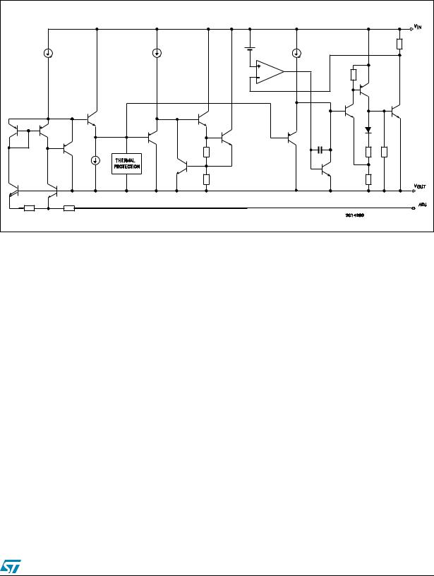
1 Diagram
Figure 1. Schematic diagram
3/28

Pin configuration |
LD1085xx |
|
|
2 Pin configuration
Figure 2. Pin connections (top view)
TO-220 |
TO-220FP |
D2PAK |
D2PAK/A |
|
DPAK |
4/28

LD1085xx |
Maximum ratings |
|
|
3 Maximum ratings
Table 2. |
Absolute maximum ratings |
|
|
|
|
|
|
|
|
||
Symbol |
Parameter |
|
|
|
|
Value |
|
Unit |
|||
|
|
|
|
|
|
|
|
|
|
|
|
VI |
|
DC input voltage |
|
|
|
|
30 |
|
V |
||
IO |
|
Output current |
|
|
Internally limited |
|
mA |
||||
PD |
|
Power dissipation |
|
|
Internally limited |
|
mW |
||||
TSTG |
|
Storage temperature range |
|
|
|
-55 to +150 |
|
°C |
|||
TOP |
|
Operating junction temperature range |
|
|
|
-40 to +125 |
|
°C |
|||
Note: |
Absolute maximum ratings are those values beyond which damage to the device may occur. |
||||||||||
|
|
Functional operation under these condition is not implied |
|
|
|
|
|
|
|||
Table 3. |
Thermal data |
|
|
|
|
|
|
|
|
||
|
|
|
|
|
|
|
|
|
|
|
|
Symbol |
|
|
Parameter |
TO-220 |
|
DPAK |
|
D2PAK |
|
Unit |
|
|
|
|
|
D2PAK/A |
|
||||||
|
|
|
|
|
|
|
|
|
|
|
|
|
|
|
|
|
|
|
|
|
|
|
|
RthJC |
|
Thermal resistance junction-case |
3 |
|
8 |
|
|
3 |
|
°C/W |
|
RthJA |
|
Thermal resistance junction-ambient |
50 |
|
100 |
|
|
62.5 |
|
°C/W |
|
5/28
Schematic application |
LD1085xx |
|
|
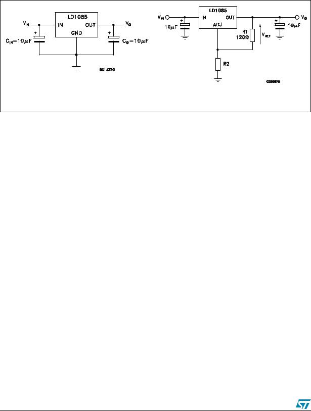
4 Schematic application
Figure 3. Application circuit
V |
|
= |
V |
|
|
R2 |
|
O |
REF |
1 + ------ |
|||||
|
|
|
|
R |
|
||
|
|
|
|
|
|
1 |
|
6/28

LD1085xx |
|
Electrical characteristics |
||||
|
|
|
|
|
|
|
5 |
Electrical characteristics |
|
|
|
|
|
Table 4. |
Electrical characteristics of LD1085#15 |
|
|
|
|
|
|
(VI = 4.5 V, CI = CO =10 µF, TA = -40 to 125 °C, unless otherwise specified). |
|
|
|||
Symbol |
Parameter |
Test condition |
Min. |
Typ. |
Max. |
Unit |
|
|
|
|
|
|
|
V |
Output voltage (1) |
IO = 0 mA, TJ = 25°C |
1.485 |
1.5 |
1.515 |
V |
|
|
|
|
|
||
O |
|
IO = 0 to 3 A, VI = 3.1 to 30 V |
1.47 |
1.5 |
1.53 |
V |
|
|
|||||
VO |
Line regulation |
IO = 0 mA, VI = 3.1 to 18 V, TJ = 25°C |
|
0.2 |
4 |
mV |
IO = 0 mA, VI = 3.1 to 15 V |
|
0.4 |
4 |
mV |
||
|
|
|
||||
VO |
Load regulation |
IO = 0 to 3 A, TJ = 25°C |
|
2 |
10 |
mV |
IO = 0 to 3 A |
|
4 |
20 |
mV |
||
|
|
|
||||
Vd |
Dropout voltage |
IO =3 A |
|
1.3 |
1.5 |
V |
Iq |
Quiescent current |
VI ≤ 30 V |
|
5 |
10 |
mA |
Isc |
Short circuit current |
VI - VO = 5 V |
3.2 |
4.5 |
|
A |
VI - VO = 25 V |
0.2 |
0.5 |
|
A |
||
|
|
|
||||
|
Thermal regulation |
TA = 25°C, 30ms pulse |
|
0.008 |
0.04 |
%/W |
SVR |
Supply voltage rejection |
f = 120 Hz, CO = 25 µF, IO = 3 A |
60 |
72 |
|
dB |
|
|
VI = 7.5 ± 3 V |
|
|
|
|
eN |
RMS output noise voltage (% |
TA = 25°C, f =10 Hz to 10 kHz |
|
0.003 |
|
% |
of VO) |
|
|
||||
|
|
|
|
|
|
|
S |
Temperature stability |
|
|
0.5 |
|
% |
|
|
|
|
|
|
|
S |
Long term stability |
TA = 125°C, 1000Hrs |
|
0.5 |
|
% |
1. See short-circuit current curve for available output current at fixed dropout.
7/28

Electrical characteristics |
|
|
|
LD1085xx |
||
|
|
|
|
|
|
|
Table 5. |
Electrical characteristics of LD1085#18 |
|
|
|
|
|
|
(VI = 4.8 V, CI = CO =10 µF, TA = -40 to 125 °C, unless otherwise specified). |
|
|
|||
Symbol |
Parameter |
Test condition |
Min. |
Typ. |
Max. |
Unit |
|
|
|
|
|
|
|
V |
Output voltage (1) |
IO = 0 mA, TJ = 25°C |
1.782 |
1.8 |
1.818 |
V |
|
|
|
|
|
||
O |
|
IO = 0 to 3 A, VI = 3.4 to 30 V |
1.764 |
1.8 |
1.836 |
V |
|
|
|||||
VO |
Line regulation |
IO = 0 mA, VI = 3.4 to 18 V TJ = 25°C |
|
0.2 |
4 |
mV |
IO = 0 mA, VI = 3.4 to 15 V |
|
0.4 |
4 |
mV |
||
|
|
|
||||
VO |
Load regulation |
IO = 0 to 3 A, TJ = 25°C |
|
2 |
10 |
mV |
IO = 0 to 3 A |
|
4 |
20 |
mV |
||
|
|
|
||||
Vd |
Dropout voltage |
IO = 3 A |
|
1.3 |
1.5 |
V |
Iq |
Quiescent current |
VI ≤ 30 V |
|
5 |
10 |
mA |
Isc |
Short circuit current |
VI - VO = 5 V |
3.2 |
4.5 |
|
A |
VI - VO = 25 V |
0.2 |
0.5 |
|
A |
||
|
|
|
||||
|
Thermal regulation |
TA = 25°C, 30 ms pulse |
|
0.008 |
0.04 |
%/W |
SVR |
Supply voltage rejection |
f = 120 Hz, CO = 25 µF, IO = 3 A |
60 |
72 |
|
dB |
|
|
VI = 7.5 ± 3 V |
|
|
|
|
eN |
RMS output noise voltage (% of |
T = 25°C, f =10 Hz to 10 kHz |
|
0.003 |
|
% |
|
VO) |
A |
|
|
|
|
|
|
|
|
|
|
|
S |
Temperature stability |
|
|
0.5 |
|
% |
|
|
|
|
|
|
|
S |
Long term stability |
TA = 125°C, 1000 Hrs |
|
0.5 |
|
% |
1. See short-circuit current curve for available output current at fixed dropout.
8/28

LD1085xx |
|
Electrical characteristics |
||||
|
|
|
|
|
|
|
Table 6. |
Electrical characteristics of LD1085#25 |
|
|
|
|
|
|
(VI = 5.5 V, CI = CO =10 µF, TA = -40 to 125 °C, unless otherwise specified). |
|
|
|||
Symbol |
Parameter |
Test condition |
Min. |
Typ. |
Max. |
Unit |
|
|
|
|
|
|
|
V |
Output voltage (1) |
IO = 0 mA, TJ = 25°C |
2.475 |
2.5 |
2.525 |
V |
|
|
|
|
|
||
O |
|
IO = 0 to 3 A, VI = 4.1 to 30 V |
2.45 |
2.5 |
2.55 |
V |
|
|
|||||
VO |
Line regulation |
IO = 0 mA, VI = 4.1 to 18 V, TJ = 25°C |
|
0.2 |
4 |
mV |
IO = 0 mA, VI = 4.1 to 18 V |
|
0.4 |
4 |
mV |
||
|
|
|
||||
VO |
Load regulation |
IO = 0 to 3 A, TJ = 25°C |
|
2 |
10 |
mV |
IO = 0 to 3 A |
|
4 |
20 |
mV |
||
|
|
|
||||
Vd |
Dropout voltage |
IO = 3 A |
|
1.3 |
1.5 |
V |
Iq |
Quiescent current |
VI ≤ 30 V |
|
5 |
10 |
mA |
Isc |
Short circuit current |
VI - VO = 5 V |
3.2 |
4.5 |
|
A |
VI - VO = 25 V |
0.2 |
0.5 |
|
A |
||
|
|
|
||||
|
Thermal regulation |
TA = 25°C, 30ms pulse |
|
0.008 |
0.04 |
%/W |
SVR |
Supply voltage rejection |
f = 120 Hz, CO = 25µF, IO = 3 A |
60 |
72 |
|
dB |
|
|
VI = 7.5 ± 3 V |
|
|
|
|
eN |
RMS output noise voltage (% |
TA = 25°C, f =10 Hz to 10 kHz |
|
0.003 |
|
% |
of VO) |
|
|
||||
|
|
|
|
|
|
|
S |
Temperature stability |
|
|
0.5 |
|
% |
|
|
|
|
|
|
|
S |
Long term stability |
TA = 125°C, 1000 Hrs |
|
0.5 |
|
% |
1. See short-circuit current curve for available output current at fixed dropout.
9/28
Loading...