


M24C16
查询M2408WBN3TG/S供应商
16Kbit, 8Kbit, 4Kbit, 2Kbit and 1Kbit Serial I²C bus EEPROM
Feature summary
■ Two-wire I²C serial interface
Supports 400kHz protocol
■ Single supply voltage:
– 2.5 to 5.5V for M24Cxx-W
– 1.8 to 5.5V for M24Cxx-R
■ Write Control input
■ Byte and Page Write (up to 16 Bytes)
■ Random and Sequential Read modes
■ Self-timed programming cycle
■ Automatic address incrementing
■ Enhanced ESD/latch-up protection
■ More than 1 million Write cycles
■ More than 40-year data retention
■ Packages
– ECOPACK® (RoHS compliant)
Table 1. Product list
Reference Part Number
M24C16, M24C08
M24C04, M24C02, M24C01
PDIP8 (BN)
SO8 (MN)
150 mil width
TSSOP8 (DW)
169 mil width
M24C16
M24C08
M24C04
M24C02
M24C01
September 2006 Rev 8 1/33
M24C16-W
M24C16-R
M24C08-W
M24C08-R
M24C04-W
M24C04-R
M24C02-W
M24C02-R
M24C01-W
M24C01-R
TSSOP8 (DS)
3x3mm² body size
UFDFPN8 (MB)
2x3mm² (MLP)
www.st.com
1

Contents M24C16, M24C08, M24C04, M24C02, M24C01
Contents
1 Summary description . . . . . . . . . . . . . . . . . . . . . . . . . . . . . . . . . . . . . . . . 6
2 Signal description . . . . . . . . . . . . . . . . . . . . . . . . . . . . . . . . . . . . . . . . . . . 8
2.1 Serial Clock (SCL) . . . . . . . . . . . . . . . . . . . . . . . . . . . . . . . . . . . . . . . . . . . 8
2.2 Serial Data (SDA) . . . . . . . . . . . . . . . . . . . . . . . . . . . . . . . . . . . . . . . . . . . . 8
2.3 Chip Enable (E0, E1, E2) . . . . . . . . . . . . . . . . . . . . . . . . . . . . . . . . . . . . . . 8
2.3.1 Write Control (WC) . . . . . . . . . . . . . . . . . . . . . . . . . . . . . . . . . . . . . . . . . 8
2.4 Supply voltage (VCC) . . . . . . . . . . . . . . . . . . . . . . . . . . . . . . . . . . . . . . . . . 9
2.4.1 Operating supply voltag e V
2.4.2 Power-up and device Reset . . . . . . . . . . . . . . . . . . . . . . . . . . . . . . . . . . . 9
2.4.3 Power-down . . . . . . . . . . . . . . . . . . . . . . . . . . . . . . . . . . . . . . . . . . . . . . . 9
CC . . . . . . . . . . . . . . . . . . . . . . . . . . . . . . . . . . . . . . . . . .9
3 Device operation . . . . . . . . . . . . . . . . . . . . . . . . . . . . . . . . . . . . . . . . . . . 11
3.1 Start condition . . . . . . . . . . . . . . . . . . . . . . . . . . . . . . . . . . . . . . . . . . . . . 11
3.2 Stop condition . . . . . . . . . . . . . . . . . . . . . . . . . . . . . . . . . . . . . . . . . . . . . 11
3.3 Acknowledge Bit (ACK) . . . . . . . . . . . . . . . . . . . . . . . . . . . . . . . . . . . . . . 11
3.4 Data input . . . . . . . . . . . . . . . . . . . . . . . . . . . . . . . . . . . . . . . . . . . . . . . . . 11
3.5 Memory addressing . . . . . . . . . . . . . . . . . . . . . . . . . . . . . . . . . . . . . . . . . 12
3.6 Write operations . . . . . . . . . . . . . . . . . . . . . . . . . . . . . . . . . . . . . . . . . . . . 13
3.6.1 Byte Write . . . . . . . . . . . . . . . . . . . . . . . . . . . . . . . . . . . . . . . . . . . . . . . 13
3.6.2 Page Write . . . . . . . . . . . . . . . . . . . . . . . . . . . . . . . . . . . . . . . . . . . . . . . 14
3.6.3 Minimizing system delays by polling on ACK . . . . . . . . . . . . . . . . . . . . . 15
3.7 Read operations . . . . . . . . . . . . . . . . . . . . . . . . . . . . . . . . . . . . . . . . . . . . 16
3.7.1 Random Address Read . . . . . . . . . . . . . . . . . . . . . . . . . . . . . . . . . . . . . 16
3.7.2 Current Address Read . . . . . . . . . . . . . . . . . . . . . . . . . . . . . . . . . . . . . . 17
3.7.3 Sequential Read . . . . . . . . . . . . . . . . . . . . . . . . . . . . . . . . . . . . . . . . . . 17
3.7.4 Acknowledge in Read mode . . . . . . . . . . . . . . . . . . . . . . . . . . . . . . . . . 17
4 Initial delivery state . . . . . . . . . . . . . . . . . . . . . . . . . . . . . . . . . . . . . . . . . 18
5 Maximum rating . . . . . . . . . . . . . . . . . . . . . . . . . . . . . . . . . . . . . . . . . . . . 18
6 DC and AC parameters . . . . . . . . . . . . . . . . . . . . . . . . . . . . . . . . . . . . . . 19
2/33

M24C16, M24C08, M24C04, M24C02, M24C01 Contents
7 Package mechanical . . . . . . . . . . . . . . . . . . . . . . . . . . . . . . . . . . . . . . . . 25
8 Part numbering . . . . . . . . . . . . . . . . . . . . . . . . . . . . . . . . . . . . . . . . . . . . 30
9 Revision history . . . . . . . . . . . . . . . . . . . . . . . . . . . . . . . . . . . . . . . . . . . 31
3/33

List of tables M24C16, M24C08, M24C04, M24C02, M24C01
List of tables
Table 1. Product list . . . . . . . . . . . . . . . . . . . . . . . . . . . . . . . . . . . . . . . . . . . . . . . . . . . . . . . . . . . . . . 1
Table 2. Signal names . . . . . . . . . . . . . . . . . . . . . . . . . . . . . . . . . . . . . . . . . . . . . . . . . . . . . . . . . . . . 6
Table 3. Device select code . . . . . . . . . . . . . . . . . . . . . . . . . . . . . . . . . . . . . . . . . . . . . . . . . . . . . . . 10
Table 4. Operating modes . . . . . . . . . . . . . . . . . . . . . . . . . . . . . . . . . . . . . . . . . . . . . . . . . . . . . . . . 12
Table 5. Absolute maximum ratings . . . . . . . . . . . . . . . . . . . . . . . . . . . . . . . . . . . . . . . . . . . . . . . . . 18
Table 6. Operating conditions (M24Cxx-W) . . . . . . . . . . . . . . . . . . . . . . . . . . . . . . . . . . . . . . . . . . . 19
Table 7. Operating conditions (M24Cxx-R) . . . . . . . . . . . . . . . . . . . . . . . . . . . . . . . . . . . . . . . . . . . 19
Table 8. DC characteristics (M24Cxx-W, Device Grade 6). . . . . . . . . . . . . . . . . . . . . . . . . . . . . . . . 19
Table 9. DC characteristics (M24Cxx-W, Device Grade 3). . . . . . . . . . . . . . . . . . . . . . . . . . . . . . . . 20
Table 10. DC characteristics (M24Cxx-R) . . . . . . . . . . . . . . . . . . . . . . . . . . . . . . . . . . . . . . . . . . . . . 20
Table 11. AC measurement conditions. . . . . . . . . . . . . . . . . . . . . . . . . . . . . . . . . . . . . . . . . . . . . . . . 21
Table 12. Input parameters. . . . . . . . . . . . . . . . . . . . . . . . . . . . . . . . . . . . . . . . . . . . . . . . . . . . . . . . . 21
Table 13. AC characteristics (M24Cxx-W) . . . . . . . . . . . . . . . . . . . . . . . . . . . . . . . . . . . . . . . . . . . . . 22
Table 14. AC characteristics (M24Cxx-R). . . . . . . . . . . . . . . . . . . . . . . . . . . . . . . . . . . . . . . . . . . . . . 23
Table 15. PDIP8 – 8 pin Plastic DIP, 0.25mm lead frame, package mechanical data . . . . . . . . . . . . 25
Table 16. SO8 narrow – 8 lead Plastic Small Outline, 150 mils body width,
package mechanical data . . . . . . . . . . . . . . . . . . . . . . . . . . . . . . . . . . . . . . . . . . . . . . . . . . 26
Table 17. UFDFPN8 (MLP8) 8-lead Ultra thin Fine pitch Dual Fla t Package No lead
2x3mm², data . . . . . . . . . . . . . . . . . . . . . . . . . . . . . . . . . . . . . . . . . . . . . . . . . . . . . . . . . . . 2 7
Table 18. TSSOP8 – 8 lead Thin Shrink Small Outline, package mechanical data . . . . . . . . . . . . . . 28
Table 19. TSSOP8 3x3mm² – 8 lead Thin Shrink Small Outline, 3x3mm² body size,
mechanical data . . . . . . . . . . . . . . . . . . . . . . . . . . . . . . . . . . . . . . . . . . . . . . . . . . . . . . . . . 29
Table 20. Ordering information scheme . . . . . . . . . . . . . . . . . . . . . . . . . . . . . . . . . . . . . . . . . . . . . . . 30
Table 21. Document revision history . . . . . . . . . . . . . . . . . . . . . . . . . . . . . . . . . . . . . . . . . . . . . . . . . 31
4/33

M24C16, M24C08, M24C04, M24C02, M24C01 List of figures
List of figures
Figure 1. Logic diagram . . . . . . . . . . . . . . . . . . . . . . . . . . . . . . . . . . . . . . . . . . . . . . . . . . . . . . . . . . . . 6
Figure 2. 8-pin package connections (top view) . . . . . . . . . . . . . . . . . . . . . . . . . . . . . . . . . . . . . . . . . 7
Figure 3. Device select code . . . . . . . . . . . . . . . . . . . . . . . . . . . . . . . . . . . . . . . . . . . . . . . . . . . . . . . . 8
Figure 4. Maximum R
Figure 5. I²C bus protocol . . . . . . . . . . . . . . . . . . . . . . . . . . . . . . . . . . . . . . . . . . . . . . . . . . . . . . . . . 10
Figure 6. Write mode sequences with WC
Figure 7. Write mode sequences with WC
Figure 8. Write cycle polling flowchart using ACK . . . . . . . . . . . . . . . . . . . . . . . . . . . . . . . . . . . . . . . 15
Figure 9. Read mode sequences. . . . . . . . . . . . . . . . . . . . . . . . . . . . . . . . . . . . . . . . . . . . . . . . . . . . 16
Figure 10. AC measurement I/O waveform . . . . . . . . . . . . . . . . . . . . . . . . . . . . . . . . . . . . . . . . . . . . . 21
Figure 11. AC waveforms . . . . . . . . . . . . . . . . . . . . . . . . . . . . . . . . . . . . . . . . . . . . . . . . . . . . . . . . . . 24
Figure 12. PDIP8 – 8 pin Plastic DIP, 0.25mm lead frame, package outline. . . . . . . . . . . . . . . . . . . . 25
Figure 13. SO8 narrow – 8 lead Plastic Small Outline, 150 mils body width, package outline . . . . . . 26
Figure 14. UFDFPN8 (MLP8) 8-lead Ultra thin Fine pitch Dual Flat Package No lead
2x3mm², outline . . . . . . . . . . . . . . . . . . . . . . . . . . . . . . . . . . . . . . . . . . . . . . . . . . . . . . . . . 27
Figure 15. TSSOP8 – 8 lead Thin Shrink Small Outline, package outline. . . . . . . . . . . . . . . . . . . . . . 28
Figure 16. TSSOP8 3x3mm² – 8 lead Thin Shrink Small Outline, 3x3mm² body size,
package outline. . . . . . . . . . . . . . . . . . . . . . . . . . . . . . . . . . . . . . . . . . . . . . . . . . . . . . . . . . 29
value versus bus parasitic capacitance (C) for an I²C bus . . . . . . . . . . . . . . 9
P
= 1 (data write inhibited) . . . . . . . . . . . . . . . . . . . . . . . . . 13
= 0 (data write enabled) . . . . . . . . . . . . . . . . . . . . . . . . . 14
5/33
Summary description M24C16, M24C08, M24C04, M24C02, M24C01
1 Summary description
These I²C-compatible electrically erasable programmable memory (EEPROM) devices are
organized as 2048/1024/512/256/128 x 8 (M24C16, M24C08, M24C04, M24C02 and
M24C01).
In order to meet environmental requirements, ST offers these devices in ECOPACK®
packages.
ECOPA CK® packages are Lead-free and RoHS compliant.
ECOPACK is an ST trademark. ECOPACK specifications are available at: www.st.com.
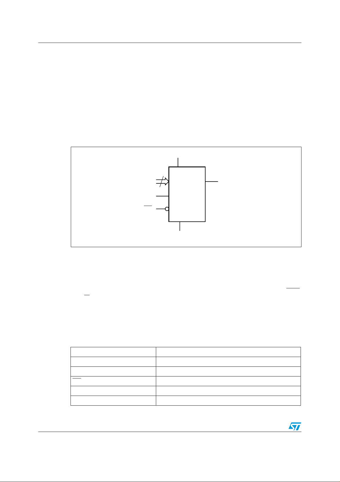
Figure 1. Logic diagram
V
CC
3
E0-E2 SDA
SCL
WC
M24Cxx
V
SS
AI02033
I²C uses a two-wire serial interface, comprising a bi-directional data line and a clock line.
The devices carry a built-in 4-bit Device Type Identifier code (1010) in accordance with the
I²C bus definition.
The device behaves as a slave in the I²C protocol, with all memory operations synchronized
by the serial clock. Read and Write operations are initiated by a Start condition, generated
by the bus master. The Start condition is followed by a Device Select Code and Read/Write
bit (RW
When writing data to the memory, the device inserts an acknowledge bit during the 9
) (as described in Table 3), terminated by an acknowledge bit.
th
bit
time, follo wing the b us master ’ s 8-bit transmission. When data is read b y the b us master, the
bus master acknowledges the receipt of the data byte in the same way. Data transfers are
terminated by a Stop condition after an Ack for Write, and after a NoAck for Read.
Table 2. Signal names
E0, E1, E2 Chip Enable
SDA Serial Data
SCL Serial Clock
WC
V
CC
V
SS
6/33
Write Control
Supply Voltage
Ground

M24C16, M24C08, M24C04, M24C02, M24C01 Summary description
Figure 2. 8-pin package connections (top view)
M24Cxx
/2Kb/4Kb/8Kb16Kb
/1Kb
/ E0/ NC/ NCNC
/ E1/ E1/ NCNC
/ E2/ E2/ E2NC
1. NC = Not Connected
2. See Section7: Package mechanical for package dimensions, and how to identify pin-1.
/ E0
/ E1
/ E2
SS
1
2
3
4
V
8
CC
WC
7
SCL
6
SDAV
5
AI02034E
7/33
Signal description M24C16, M24C08, M24C04, M24C02, M24C01
2 Signal description
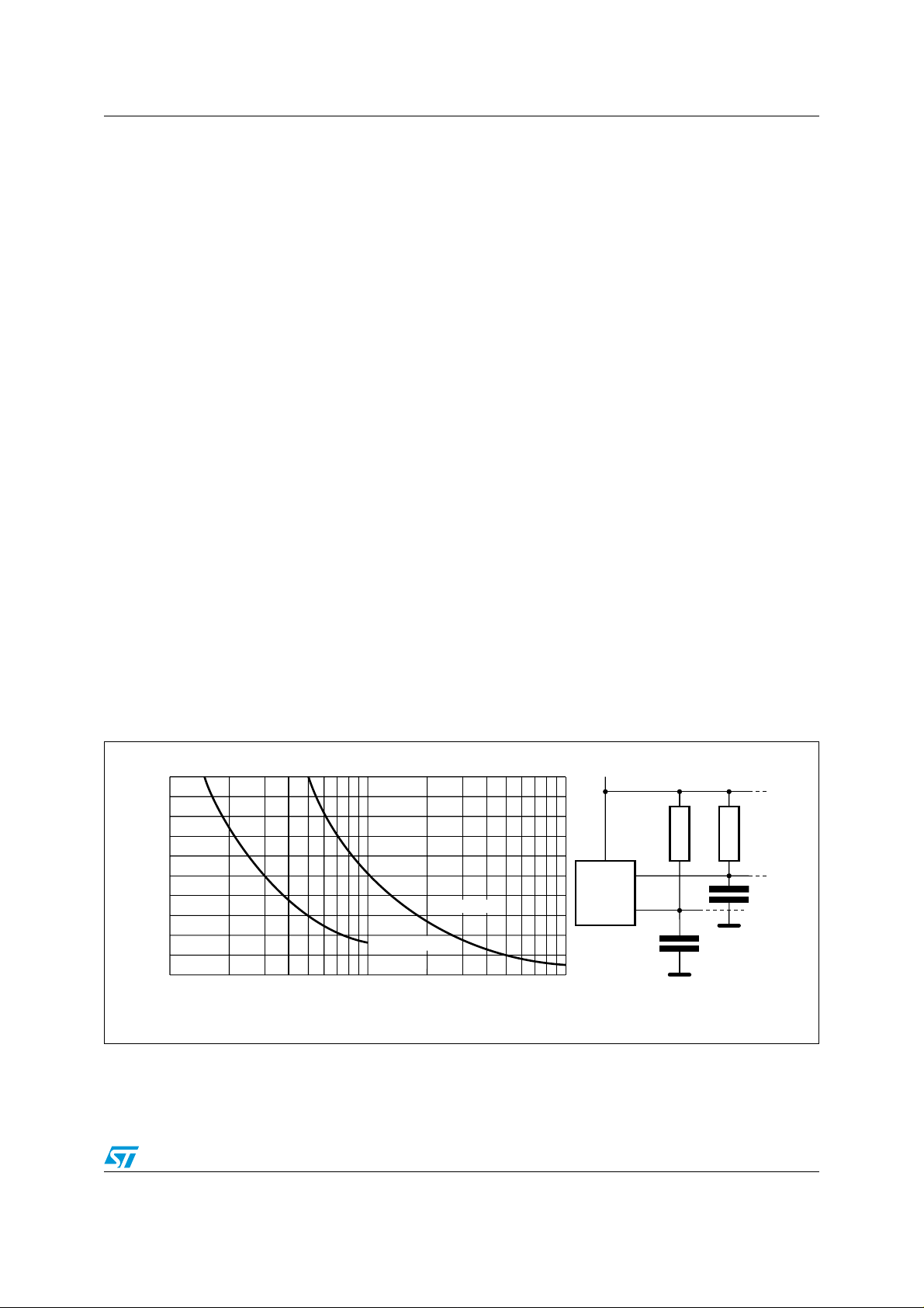
2.1 Serial Clock (SCL)
This input signal is used to strobe all data in and out of the device. In applications where this
signal is used by slave devices to synchronize the bus to a slower clock, the bus master
must have an open drain output, and a pull-up resistor can be connected from Serial Clock
(SCL) to V
most applications, though, this method of synchronization is not employed , and so the pullup resistor is not necessary, provided that the bus master has a push-pull (rather than op en
drain) output.
2.2 Serial Data (SDA)
This bi-directional signal is used to transfer data in or out of the device. It is an open drain
output that may be wire-OR’ed with other op en dr ain or open collector signa ls on the b u s . A
pull up resistor must be connected from Serial Data (SDA) to V
the value of the pull-up resistor can be calculated).
. (Figure 4 indicates how the value of the pull-up resistor can be calculated). In
CC
. (Figure 4 indicates how
CC
2.3 Chip Enable (E0, E1, E2)
These input signals are used to set the value that is to be looked for on the three least
significant bits (b3, b2, b1) of the 7-bit Device Select Code. These inputs must be tied to
V
or VSS, to establish the Device Select Code as shown in Figure 3.
CC
Figure 3. Device select code
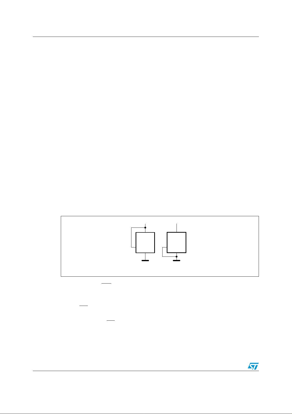
2.3.1 Write Control (WC)
This input signal is useful for protecting the entire contents of the memory from inadvertent
write operations. Write operations are disabled to the entire memory array when Write
Control (WC
Write operations are allowed.
) is driven High. When unconnected, the signal is internally read as VIL, and
V
CC
M24Cxx
E
i
V
SS
V
CC
M24Cxx
E
i
V
SS
Ai11650
When Write Control (WC
) is driven High, Device Select and Address bytes are
acknowledged, Da ta bytes are not acknowledged .
8/33
M24C16, M24C08, M24C04, M24C02, M24C01 Signal description
2.4 Supply voltage (VCC)
2.4.1 Operating supply voltage V
Prior to selecting the memory and issuing instructions to it, a valid and stable VCC voltage
within the specified [V
(min), VCC(max)] range must be applied (see Table 6 and Table 7).
CC
In order to secure a stable DC supply voltage, it is recommended to decouple the V
with a suitable capacitor (usually of the order of 10nF to 100nF) close to the V
package pins.
This voltage must remain stab le and v a lid until the end o f the tr ansm ission of the instruction
and, for a Write instruction, until the completion of the internal write cycle (t
The V
rise time must not vary faster than 1V/µs
CC
2.4.2 Power-up and device Reset
In order to prevent inadvertent Write operations during Power-up, a Power On Reset (POR)
circuit is included. At P o wer -up (contin uous rise of V
instruction until V
lower than the minimum V
When V
has passed the POR threshold, the device is reset and in Standby Power mode.
CC
has reached the Power On Reset threshold voltage (this threshold is
CC
operating voltage defined in Table 6 and Table 7).
CC
2.4.3 Power-down
At Power-down (where VCC decreases continuously), as soon as VCC drops from the
operating voltage range to below the Power On Reset threshold voltage, the device stops
responding to any instruction sent to it.
CC
CC
CC/VSS
).
W
), the device does not r espond to an y
CC
line
During Pow er-do wn, the device must be deselected and in the Stan db y Power mode (tha t is
there should be no internal Write cycle in progress).
Figure 4. Maximum R
20
16
12
8
Maximum RP value (kΩ)
4
0
10
value versus bus parasitic capacitance (C) for an I²C bus
P
V
CC
SDA
fc = 400kHz
100
C (pF)
fc = 100kHz
MASTER
1000
SCL
R
R
P
P
C
C
AI01665b
9/33
Signal description M24C16, M24C08, M24C04, M24C02, M24C01
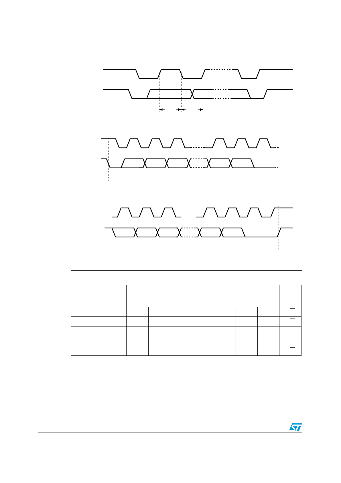
Figure 5. I²C bus protocol
SCL
SDA
SCL
SDA
SCL
SDA
START
Condition
START
Condition
1 23 7 89
MSB
1 23 7 89
MSB ACK
SDA
Input
SDA
Change
STOP
Condition
ACK
STOP
Condition
AI00792B
Table 3. Device select code
Device Type Identifier
b7 b6 b5 b4 b3 b2 b1 b0
M24C01 Select Code1010E2E1E0RW
M24C02 Select Code1010E2E1E0RW
M24C04 Select Code1010E2E1A8RW
M24C08 Select Code1010E2A9A8RW
M24C16 Select Code1010A10A9A8RW
1. The most significant bit, b7, is sent first.
2. E0, E1 and E2 are compared against the respective external pins on the memory device.
3. A10, A9 and A8 represent most significant bits of the address.
10/33
(1)
Chip Enable
(2),(3)
RW
 Loading...