


STM32F302CB
Table of contents
 Loading...
ST STM32F302CB, STM32F302CC, STM32F302RB, STM32F302RC, STM32F302VB User Manual
...
STM32F302xx STM32F303xx
LQFP64 (10 × 10 mm)
LQFP100 (14 × 14 mm)
LQFP48 (7 × 7 mm)
ARM™Cortex-M4 32b MCU+FPU, up to 256KB Flash+48KB SRAM
4 ADCs, 2 DAC ch., 7 comp., 4 PGA, timers, 2.0-3.6 V operation
Datasheet − preliminary data
Features
■ ARM 32-bit Cortex®-M4 CPU (72 MHz max),
single-cycle multiplication and HW division, DSP
instruction with FPU (floating-point unit) and MPU
(memory protection unit).
■ Operating conditions:
, V
–V
DD
■ Memories
voltage range: 2.0 V to 3.6 V
DDA
– 128 to 256 Kbytes of Flash memory
– Up to 40 Kbytes of SRAM on data bus with
HW parity check
– 8 Kbytes of SRAM on instruction bus with HW
parity check (CCM)
■ Clock management
– 4 to 32 MHz crystal oscillator
– 32 kHz oscillator for RTC with calibration
– Internal 8 MHz RC with x 16 PLL option
– Internal 40 kHz oscillator
■ Calendar RTC
– Alarm, periodic wakeup from Stop/Standby
■ Reset and supply management
– Power-on/Power down reset (POR/PDR)
– Programmable voltage detector (PVD)
■ Low power Sleep, Stop, and Standby modes
■ V
■ Debug mode: serial wire debug (SWD), JTAG
supply for RTC and backup registers
BAT
interfaces, Cortex-M4 ETM
■ DMA
– 12-channel DMA controller
– Peripherals supported: timers, ADCs, SPIs,
2
Cs, USARTs and DACs
I
■ Up to 4 × ADC 0.20 µS (up to 39 channels) with
selectable resolution of 12/10/8/6 bits, 0 to 3.6 V
conversion range, separate analog supply from 2
to 3.6 V
■ Temperature sensor
■ 7 fast rail-to-rail analog comparators
■ Up to 2 x 12-bit DAC channels
■ Up to 4 operational amplifiers that can be used in
PGA mode, all terminal accessible
■ Support for up to 24 capacitive sensing keys
■ Up to 87 fast I/O ports, all mappable on external
interrupt vectors, several 5 V-tolerant
■ Up to 13 timers
– 1 x 32-bit timer and 2 x 16-bit timers with up
to 4 IC/OC/PWM or pulse counter and
quadrature (incremental) encoder input
– Up to 2 x 16-bit 6-channel advanced-control
timers, with up to 6 PWM channels, deadtime
generation and emergency stop
– 1 x 16-bit timer with 2 IC/OCs, 1 OCN/PWM,
deadtime generation and emergency stop
– 2 x 16-bit timers with IC/OC/OCN/PWM,
deadtime generation and emergency stop
– 2 x watchdog timers (independent, window)
– 1 x SysTick timer: 24-bit downcounter
– Up to 2 x 16-bit basic timers to drive the DAC
■ Communication interfaces
– CAN interface (2.0B Active)
– USB 2.0 full speed interface
– 2 x I2C with 20 mA current sink to support
Fast mode plus
– Up to 5 USART/UARTs (ISO 7816 interface,
LIN, IrDA, modem control)
– Up to 3 SPIs, 2 with muxed full-duplex I2S to
achieve audio class accuracy via external
PLL
■ CRC calculation unit, 96-bit unique ID
Table 1. Device summary
Reference Part number
STM32F302xx
STM32F303xx
STM32F302CB, STM32F302CC, STM32F302RB,
STM32F302RC, STM32F302VB, STM32F302VC
STM32F303CB, STM32F303CC, STM32F303RB,
STM32F303RC, STM32F303VB, STM32F303VC
June 2012 Doc ID 023353 Rev 1 1/119
This is preliminary information on a new product now in development or undergoing evaluation. Details are subject to
change without notice.
www.st.com
1

Contents STM32F302xx/STM32F303xx
Contents
1 Description . . . . . . . . . . . . . . . . . . . . . . . . . . . . . . . . . . . . . . . . . . . . . . . . . 8
2 Device overview . . . . . . . . . . . . . . . . . . . . . . . . . . . . . . . . . . . . . . . . . . . 10
3 Functional overview . . . . . . . . . . . . . . . . . . . . . . . . . . . . . . . . . . . . . . . . 13
3.1 ARM® Cortex™-M4 core with embedded Flash and SRAM . . . . . . . . . . 13
3.2 Memory protection unit . . . . . . . . . . . . . . . . . . . . . . . . . . . . . . . . . . . . . . . 13
3.3 Nested vectored interrupt controller (NVIC) . . . . . . . . . . . . . . . . . . . . . . . 14
3.4 Embedded Flash memory . . . . . . . . . . . . . . . . . . . . . . . . . . . . . . . . . . . . 14
3.5 CRC (cyclic redundancy check) calculation unit . . . . . . . . . . . . . . . . . . . 14
3.6 Embedded SRAM . . . . . . . . . . . . . . . . . . . . . . . . . . . . . . . . . . . . . . . . . . . 14
3.7 Clocks and startup . . . . . . . . . . . . . . . . . . . . . . . . . . . . . . . . . . . . . . . . . . 15
3.8 Boot modes . . . . . . . . . . . . . . . . . . . . . . . . . . . . . . . . . . . . . . . . . . . . . . . 15
3.9 Power supply schemes . . . . . . . . . . . . . . . . . . . . . . . . . . . . . . . . . . . . . . . 15
3.10 Power supply supervisor . . . . . . . . . . . . . . . . . . . . . . . . . . . . . . . . . . . . . 15
3.11 Voltage regulator . . . . . . . . . . . . . . . . . . . . . . . . . . . . . . . . . . . . . . . . . . . 16
3.12 Low-power modes . . . . . . . . . . . . . . . . . . . . . . . . . . . . . . . . . . . . . . . . . . 16
3.13 Real-time clock (RTC) and backup registers . . . . . . . . . . . . . . . . . . . . . . 17
3.14 DMA (direct memory access) . . . . . . . . . . . . . . . . . . . . . . . . . . . . . . . . . . 17
3.15 GPIOs (general-purpose inputs/outputs) . . . . . . . . . . . . . . . . . . . . . . . . . 17
3.16 Fast ADC (analog-to-digital converter) . . . . . . . . . . . . . . . . . . . . . . . . . . . 18
3.16.1 Temperature sensor . . . . . . . . . . . . . . . . . . . . . . . . . . . . . . . . . . . . . . . . 18
3.16.2 Internal voltage reference (V
3.16.3 V
3.16.4 OPAMP reference voltage (VOPAMP) . . . . . . . . . . . . . . . . . . . . . . . . . . 19
battery voltage monitoring . . . . . . . . . . . . . . . . . . . . . . . . . . . . . . . 19
BAT
) . . . . . . . . . . . . . . . . . . . . . . . . . . . 19
REFINT
3.17 DAC (digital-to-analog converter) . . . . . . . . . . . . . . . . . . . . . . . . . . . . . . . 19
3.18 Operational amplifier . . . . . . . . . . . . . . . . . . . . . . . . . . . . . . . . . . . . . . . . 20
3.19 Fast comparators . . . . . . . . . . . . . . . . . . . . . . . . . . . . . . . . . . . . . . . . . . . 20
3.20 Timers and watchdogs . . . . . . . . . . . . . . . . . . . . . . . . . . . . . . . . . . . . . . . 20
3.20.1 Advanced timers (TIM1, TIM8) . . . . . . . . . . . . . . . . . . . . . . . . . . . . . . . 21
3.20.2 General-purpose timers (TIM2, TIM3, TIM4, TIM15, TIM16, TIM17) . . 22
3.20.3 Basic timers (TIM6, TIM7) . . . . . . . . . . . . . . . . . . . . . . . . . . . . . . . . . . . 22
2/119 Doc ID 023353 Rev 1

STM32F302xx/STM32F303xx Contents
3.20.4 Independent watchdog . . . . . . . . . . . . . . . . . . . . . . . . . . . . . . . . . . . . . 22
3.20.5 Window watchdog . . . . . . . . . . . . . . . . . . . . . . . . . . . . . . . . . . . . . . . . . 22
3.20.6 SysTick timer . . . . . . . . . . . . . . . . . . . . . . . . . . . . . . . . . . . . . . . . . . . . . 23
3.21 Communication interfaces . . . . . . . . . . . . . . . . . . . . . . . . . . . . . . . . . . . . 23
3.21.1 I2C bus . . . . . . . . . . . . . . . . . . . . . . . . . . . . . . . . . . . . . . . . . . . . . . . . . . 23
3.21.2 Universal synchronous/asynchronous receiver transmitter (USART) . . 23
3.21.3 Universal asynchronous receiver transmitter (UART) . . . . . . . . . . . . . . 24
3.21.4 Serial peripheral interface (SPI)/Inter-integrated sound interfaces (I
3.21.5 Controller area network (CAN) . . . . . . . . . . . . . . . . . . . . . . . . . . . . . . . 24
3.21.6 Universal serial bus (USB) . . . . . . . . . . . . . . . . . . . . . . . . . . . . . . . . . . . 24
2
S) 24
3.22 Touch sensing controller (TSC) . . . . . . . . . . . . . . . . . . . . . . . . . . . . . . . . 24
3.23 Development support . . . . . . . . . . . . . . . . . . . . . . . . . . . . . . . . . . . . . . . . 26
3.23.1 Serial wire JTAG debug port (SWJ-DP) . . . . . . . . . . . . . . . . . . . . . . . . . 26
3.23.2 Embedded trace macrocell™ . . . . . . . . . . . . . . . . . . . . . . . . . . . . . . . . 26
4 Pinouts and pin description . . . . . . . . . . . . . . . . . . . . . . . . . . . . . . . . . . 27
5 Memory mapping . . . . . . . . . . . . . . . . . . . . . . . . . . . . . . . . . . . . . . . . . . 47
6 Electrical characteristics . . . . . . . . . . . . . . . . . . . . . . . . . . . . . . . . . . . . 50
6.1 Parameter conditions . . . . . . . . . . . . . . . . . . . . . . . . . . . . . . . . . . . . . . . . 50
6.1.1 Minimum and maximum values . . . . . . . . . . . . . . . . . . . . . . . . . . . . . . . 50
6.1.2 Typical values . . . . . . . . . . . . . . . . . . . . . . . . . . . . . . . . . . . . . . . . . . . . . 50
6.1.3 Typical curves . . . . . . . . . . . . . . . . . . . . . . . . . . . . . . . . . . . . . . . . . . . . 50
6.1.4 Loading capacitor . . . . . . . . . . . . . . . . . . . . . . . . . . . . . . . . . . . . . . . . . 50
6.1.5 Pin input voltage . . . . . . . . . . . . . . . . . . . . . . . . . . . . . . . . . . . . . . . . . . 50
6.1.6 Power supply scheme . . . . . . . . . . . . . . . . . . . . . . . . . . . . . . . . . . . . . . 51
6.1.7 Current consumption measurement . . . . . . . . . . . . . . . . . . . . . . . . . . . 51
6.2 Absolute maximum ratings . . . . . . . . . . . . . . . . . . . . . . . . . . . . . . . . . . . . 52
6.3 Operating conditions . . . . . . . . . . . . . . . . . . . . . . . . . . . . . . . . . . . . . . . . 54
6.3.1 General operating conditions . . . . . . . . . . . . . . . . . . . . . . . . . . . . . . . . . 54
6.3.2 Operating conditions at power-up / power-down . . . . . . . . . . . . . . . . . . 55
6.3.3 Embedded reset and power control block characteristics . . . . . . . . . . . 55
6.3.4 Embedded reference voltage . . . . . . . . . . . . . . . . . . . . . . . . . . . . . . . . . 57
6.3.5 Supply current characteristics . . . . . . . . . . . . . . . . . . . . . . . . . . . . . . . . 57
6.3.6 External clock source characteristics . . . . . . . . . . . . . . . . . . . . . . . . . . . 70
6.3.7 Internal clock source characteristics . . . . . . . . . . . . . . . . . . . . . . . . . . . 75
Doc ID 023353 Rev 1 3/119

Contents STM32F302xx/STM32F303xx
6.3.8 PLL characteristics . . . . . . . . . . . . . . . . . . . . . . . . . . . . . . . . . . . . . . . . 76
6.3.9 Memory characteristics . . . . . . . . . . . . . . . . . . . . . . . . . . . . . . . . . . . . . 77
6.3.10 EMC characteristics . . . . . . . . . . . . . . . . . . . . . . . . . . . . . . . . . . . . . . . . 79
6.3.11 Electrical sensitivity characteristics . . . . . . . . . . . . . . . . . . . . . . . . . . . . 80
6.3.12 I/O current injection characteristics . . . . . . . . . . . . . . . . . . . . . . . . . . . . 81
6.3.13 I/O port characteristics . . . . . . . . . . . . . . . . . . . . . . . . . . . . . . . . . . . . . . 82
6.3.14 NRST pin characteristics . . . . . . . . . . . . . . . . . . . . . . . . . . . . . . . . . . . . 87
6.3.15 Timer characteristics . . . . . . . . . . . . . . . . . . . . . . . . . . . . . . . . . . . . . . . 88
6.3.16 Communications interfaces . . . . . . . . . . . . . . . . . . . . . . . . . . . . . . . . . . 90
6.3.17 ADC characteristics . . . . . . . . . . . . . . . . . . . . . . . . . . . . . . . . . . . . . . . . 97
6.3.18 DAC electrical specifications . . . . . . . . . . . . . . . . . . . . . . . . . . . . . . . . 101
6.3.19 Comparator characteristics . . . . . . . . . . . . . . . . . . . . . . . . . . . . . . . . . 103
6.3.20 Operational amplifer charateristics . . . . . . . . . . . . . . . . . . . . . . . . . . . 105
6.3.21 Temperature sensor characteristics . . . . . . . . . . . . . . . . . . . . . . . . . . . 107
6.3.22 V
6.3.23 USB characteristics . . . . . . . . . . . . . . . . . . . . . . . . . . . . . . . . . . . . . . . 108
monitoring characteristics . . . . . . . . . . . . . . . . . . . . . . . . . . . . . . 107
BAT
7 Package characteristics . . . . . . . . . . . . . . . . . . . . . . . . . . . . . . . . . . . . 110
7.1 Package mechanical data . . . . . . . . . . . . . . . . . . . . . . . . . . . . . . . . . . . 110
7.2 Thermal characteristics . . . . . . . . . . . . . . . . . . . . . . . . . . . . . . . . . . . . . 114
7.2.1 Reference document . . . . . . . . . . . . . . . . . . . . . . . . . . . . . . . . . . . . . . 114
7.2.2 Selecting the product temperature range . . . . . . . . . . . . . . . . . . . . . . . 115
8 Part numbering . . . . . . . . . . . . . . . . . . . . . . . . . . . . . . . . . . . . . . . . . . . 117
9 Revision history . . . . . . . . . . . . . . . . . . . . . . . . . . . . . . . . . . . . . . . . . . 118
4/119 Doc ID 023353 Rev 1

STM32F302xx/STM32F303xx List of tables
List of tables
Table 1. Device summary . . . . . . . . . . . . . . . . . . . . . . . . . . . . . . . . . . . . . . . . . . . . . . . . . . . . . . . . . . 1
Table 2. STM32F30x family device features and peripheral counts . . . . . . . . . . . . . . . . . . . . . . . . . . 9
Table 3. Temperature sensor calibration values. . . . . . . . . . . . . . . . . . . . . . . . . . . . . . . . . . . . . . . . 19
Table 4. Temperature sensor calibration values. . . . . . . . . . . . . . . . . . . . . . . . . . . . . . . . . . . . . . . . 19
Table 5. Timer feature comparison . . . . . . . . . . . . . . . . . . . . . . . . . . . . . . . . . . . . . . . . . . . . . . . . . . 21
Table 6. Comparison of I2C analog and digital filters . . . . . . . . . . . . . . . . . . . . . . . . . . . . . . . . . . . . 23
Table 7. Capacitive sensing GPIOs available on STM32F302xx/STM32F303xx
devices . . . . . . . . . . . . . . . . . . . . . . . . . . . . . . . . . . . . . . . . . . . . . . . . . . . . . . . . . . . . . . . . 25
Table 8. No. of capacitive sensing channels available on STM32F302xx/STM32F303xx devices . 26
Table 9. Legend/abbreviations used in the pinout table . . . . . . . . . . . . . . . . . . . . . . . . . . . . . . . . . . 30
Table 10. STM32F302xx/STM32F303xx pin definitions . . . . . . . . . . . . . . . . . . . . . . . . . . . . . . . . . . . 31
Table 11. Alternate functions . . . . . . . . . . . . . . . . . . . . . . . . . . . . . . . . . . . . . . . . . . . . . . . . . . . . . . . 39
Table 12. STM32F30x memory map and peripheral register boundary
addresses48
Table 13. Voltage characteristics . . . . . . . . . . . . . . . . . . . . . . . . . . . . . . . . . . . . . . . . . . . . . . . . . . . . 52
Table 14. Current characteristics . . . . . . . . . . . . . . . . . . . . . . . . . . . . . . . . . . . . . . . . . . . . . . . . . . . . 53
Table 15. Thermal characteristics. . . . . . . . . . . . . . . . . . . . . . . . . . . . . . . . . . . . . . . . . . . . . . . . . . . . 53
Table 16. General operating conditions . . . . . . . . . . . . . . . . . . . . . . . . . . . . . . . . . . . . . . . . . . . . . . . 54
Table 17. Operating conditions at power-up / power-down . . . . . . . . . . . . . . . . . . . . . . . . . . . . . . . . 55
Table 18. Embedded reset and power control block characteristics. . . . . . . . . . . . . . . . . . . . . . . . . . 55
Table 19. Programmable voltage detector characteristics . . . . . . . . . . . . . . . . . . . . . . . . . . . . . . . . . 55
Table 20. Embedded internal reference voltage . . . . . . . . . . . . . . . . . . . . . . . . . . . . . . . . . . . . . . . . . 57
Table 21. Typical and maximum current consumption from V
at V
= 3.6 V58
DD
Table 22. Typical and maximum current consumption from the V
Table 23. Typical and maximum V
Table 24. Typical and maximum V
consumption in Stop and Standby modes . . . . . . . . . . . . . . . 61
DD
consumption in Stop and Standby modes . . . . . . . . . . . . . . 61
DDA
Table 25. Typical and maximum current consumption from V
Table 26. Typical current consumption in Run mode, code with data processing
running from Flash . . . . . . . . . . . . . . . . . . . . . . . . . . . . . . . . . . . . . . . . . . . . . . . . . . . . . . . 63
Table 27. Typical current consumption in Sleep mode, code running from Flash or RAM. . . . . . . . . 64
Table 28. Switching output I/O current consumption . . . . . . . . . . . . . . . . . . . . . . . . . . . . . . . . . . . . . 66
Table 29. Peripheral current consumption . . . . . . . . . . . . . . . . . . . . . . . . . . . . . . . . . . . . . . . . . . . . . 68
Table 30. High-speed external user clock characteristics. . . . . . . . . . . . . . . . . . . . . . . . . . . . . . . . . . 70
Table 31. Low-speed external user clock characteristics . . . . . . . . . . . . . . . . . . . . . . . . . . . . . . . . . . 71
Table 32. HSE oscillator characteristics . . . . . . . . . . . . . . . . . . . . . . . . . . . . . . . . . . . . . . . . . . . . . . . 72
Table 33. LSE oscillator characteristics (f
= 32.768 kHz) . . . . . . . . . . . . . . . . . . . . . . . . . . . . . . . 74
LSE
Table 34. HSI oscillator characteristics. . . . . . . . . . . . . . . . . . . . . . . . . . . . . . . . . . . . . . . . . . . . . . . . 75
Table 35. LSI oscillator characteristics . . . . . . . . . . . . . . . . . . . . . . . . . . . . . . . . . . . . . . . . . . . . . . . . 76
Table 36. Low-power mode wakeup timings . . . . . . . . . . . . . . . . . . . . . . . . . . . . . . . . . . . . . . . . . . . 76
Table 37. PLL characteristics . . . . . . . . . . . . . . . . . . . . . . . . . . . . . . . . . . . . . . . . . . . . . . . . . . . . . . . 77
Table 38. Flash memory characteristics . . . . . . . . . . . . . . . . . . . . . . . . . . . . . . . . . . . . . . . . . . . . . . . 78
Table 39. Flash memory endurance and data retention . . . . . . . . . . . . . . . . . . . . . . . . . . . . . . . . . . . 78
Table 40. EMS characteristics . . . . . . . . . . . . . . . . . . . . . . . . . . . . . . . . . . . . . . . . . . . . . . . . . . . . . . 79
Table 41. EMI characteristics . . . . . . . . . . . . . . . . . . . . . . . . . . . . . . . . . . . . . . . . . . . . . . . . . . . . . . . 80
Table 42. ESD absolute maximum ratings . . . . . . . . . . . . . . . . . . . . . . . . . . . . . . . . . . . . . . . . . . . . . 80
Table 43. Electrical sensitivities . . . . . . . . . . . . . . . . . . . . . . . . . . . . . . . . . . . . . . . . . . . . . . . . . . . . . 81
Table 44. I/O current injection susceptibility . . . . . . . . . . . . . . . . . . . . . . . . . . . . . . . . . . . . . . . . . . . . 81
supply
DD
supply . . . . . . . . . . . . . . . . . . 60
DDA
supply. . . . . . . . . . . . . . . . . . . . . . 62
BAT
Doc ID 023353 Rev 1 5/119

List of tables STM32F302xx/STM32F303xx
Table 45. I/O static characteristics . . . . . . . . . . . . . . . . . . . . . . . . . . . . . . . . . . . . . . . . . . . . . . . . . . . 82
Table 46. Output voltage characteristics . . . . . . . . . . . . . . . . . . . . . . . . . . . . . . . . . . . . . . . . . . . . . . 85
Table 47. I/O AC characteristics . . . . . . . . . . . . . . . . . . . . . . . . . . . . . . . . . . . . . . . . . . . . . . . . . . . . . 86
Table 48. NRST pin characteristics . . . . . . . . . . . . . . . . . . . . . . . . . . . . . . . . . . . . . . . . . . . . . . . . . . 87
Table 49. TIMx characteristics . . . . . . . . . . . . . . . . . . . . . . . . . . . . . . . . . . . . . . . . . . . . . . . . . . . . . . 88
Table 50. IWDG min/max timeout period at 40 kHz (LSI) . . . . . . . . . . . . . . . . . . . . . . . . . . . . . . . . . 88
Table 51. WWDG min-max timeout value @72 MHz (PCLK). . . . . . . . . . . . . . . . . . . . . . . . . . . . . . . 89
Table 52. I
2
C characteristics. . . . . . . . . . . . . . . . . . . . . . . . . . . . . . . . . . . . . . . . . . . . . . . . . . . . . . . . 90
Table 53. I2C analog filter characteristics. . . . . . . . . . . . . . . . . . . . . . . . . . . . . . . . . . . . . . . . . . . . . . 90
Table 54. SPI characteristics . . . . . . . . . . . . . . . . . . . . . . . . . . . . . . . . . . . . . . . . . . . . . . . . . . . . . . . 92
Table 55. I
2
S characteristics . . . . . . . . . . . . . . . . . . . . . . . . . . . . . . . . . . . . . . . . . . . . . . . . . . . . . . . . 95
Table 56. ADC characteristics . . . . . . . . . . . . . . . . . . . . . . . . . . . . . . . . . . . . . . . . . . . . . . . . . . . . . . 97
Table 57. Minimum sampling time to be respected for fast and slow channels . . . . . . . . . . . . . . . . . 98
Table 58. ADC accuracy . . . . . . . . . . . . . . . . . . . . . . . . . . . . . . . . . . . . . . . . . . . . . . . . . . . . . . . . . . 99
Table 59. DAC characteristics . . . . . . . . . . . . . . . . . . . . . . . . . . . . . . . . . . . . . . . . . . . . . . . . . . . . . 101
Table 60. Comparator characteristics . . . . . . . . . . . . . . . . . . . . . . . . . . . . . . . . . . . . . . . . . . . . . . . . 103
Table 61. Operational amplifier characteristics. . . . . . . . . . . . . . . . . . . . . . . . . . . . . . . . . . . . . . . . . 105
Table 62. TS characteristics . . . . . . . . . . . . . . . . . . . . . . . . . . . . . . . . . . . . . . . . . . . . . . . . . . . . . . . 107
Table 63. V
monitoring characteristics . . . . . . . . . . . . . . . . . . . . . . . . . . . . . . . . . . . . . . . . . . . . 107
BAT
Table 64. USB startup time. . . . . . . . . . . . . . . . . . . . . . . . . . . . . . . . . . . . . . . . . . . . . . . . . . . . . . . . 108
Table 65. USB DC electrical characteristics . . . . . . . . . . . . . . . . . . . . . . . . . . . . . . . . . . . . . . . . . . . 108
Table 66. USB: Full-speed electrical characteristics. . . . . . . . . . . . . . . . . . . . . . . . . . . . . . . . . . . . . 108
Table 67. LQPF100 – 14 x 14 mm, 100-pin low-profile quad flat package mechanical data . . . . . . 111
Table 68. LQFP64 – 10 x 10 mm, 64-pin low-profile quad flat package mechanical data . . . . . . . . 112
Table 69. LQFP48 – 7 x 7 mm, 48-pin low-profile quad flat package mechanical data . . . . . . . . . . 113
Table 70. Package thermal characteristics . . . . . . . . . . . . . . . . . . . . . . . . . . . . . . . . . . . . . . . . . . . . 114
Table 71. Ordering information scheme . . . . . . . . . . . . . . . . . . . . . . . . . . . . . . . . . . . . . . . . . . . . . . 117
Table 72. Document revision history . . . . . . . . . . . . . . . . . . . . . . . . . . . . . . . . . . . . . . . . . . . . . . . . 118
6/119 Doc ID 023353 Rev 1

STM32F302xx/STM32F303xx List of figures
List of figures
Figure 1. STM32F302xx block diagram . . . . . . . . . . . . . . . . . . . . . . . . . . . . . . . . . . . . . . . . . . . . . . . 10
Figure 2. STM32F303xx block diagram . . . . . . . . . . . . . . . . . . . . . . . . . . . . . . . . . . . . . . . . . . . . . . . 11
Figure 3. Clock tree . . . . . . . . . . . . . . . . . . . . . . . . . . . . . . . . . . . . . . . . . . . . . . . . . . . . . . . . . . . . . . 12
Figure 4. STM32F302xx/STM32F303xx LQFP48 pinout . . . . . . . . . . . . . . . . . . . . . . . . . . . . . . . . . 27
Figure 5. STM32F302xx/STM32F303xx LQFP64 pinout . . . . . . . . . . . . . . . . . . . . . . . . . . . . . . . . 28
Figure 6. STM32F302xx/STM32F303xx LQFP100 pinout . . . . . . . . . . . . . . . . . . . . . . . . . . . . . . . . 29
Figure 7. STM32F30x memory map . . . . . . . . . . . . . . . . . . . . . . . . . . . . . . . . . . . . . . . . . . . . . . . . . 47
Figure 8. Pin loading conditions . . . . . . . . . . . . . . . . . . . . . . . . . . . . . . . . . . . . . . . . . . . . . . . . . . . . . 50
Figure 9. Pin input voltage . . . . . . . . . . . . . . . . . . . . . . . . . . . . . . . . . . . . . . . . . . . . . . . . . . . . . . . . . 50
Figure 10. Power supply scheme. . . . . . . . . . . . . . . . . . . . . . . . . . . . . . . . . . . . . . . . . . . . . . . . . . . . . 51
Figure 11. Current consumption measurement scheme . . . . . . . . . . . . . . . . . . . . . . . . . . . . . . . . . . . 51
Figure 12. High-speed external clock source AC timing diagram . . . . . . . . . . . . . . . . . . . . . . . . . . . . 70
Figure 13. Low-speed external clock source AC timing diagram . . . . . . . . . . . . . . . . . . . . . . . . . . . . . 71
Figure 14. Typical application with an 8 MHz crystal . . . . . . . . . . . . . . . . . . . . . . . . . . . . . . . . . . . . . . 73
Figure 15. Typical application with a 32.768 kHz crystal . . . . . . . . . . . . . . . . . . . . . . . . . . . . . . . . . . . 75
Figure 16. TC and TTa I/O input characteristics - CMOS port . . . . . . . . . . . . . . . . . . . . . . . . . . . . . . . 83
Figure 17. TC and TTa I/O input characteristics - TTL port . . . . . . . . . . . . . . . . . . . . . . . . . . . . . . . . . 83
Figure 18. Five volt tolerant (FT and FTf) I/O input characteristics - CMOS port. . . . . . . . . . . . . . . . . 84
Figure 19. Five volt tolerant (FT and FTf) I/O input characteristics - TTL port . . . . . . . . . . . . . . . . . . . 84
Figure 20. I/O AC characteristics definition . . . . . . . . . . . . . . . . . . . . . . . . . . . . . . . . . . . . . . . . . . . . . 87
Figure 21. Recommended NRST pin protection . . . . . . . . . . . . . . . . . . . . . . . . . . . . . . . . . . . . . . . . . 87
Figure 22. I
Figure 23. SPI timing diagram - slave mode and CPHA = 0 . . . . . . . . . . . . . . . . . . . . . . . . . . . . . . . . 93
Figure 24. SPI timing diagram - slave mode and CPHA = 1
Figure 25. SPI timing diagram - master mode
Figure 26. I
Figure 27. I
Figure 28. ADC accuracy characteristics . . . . . . . . . . . . . . . . . . . . . . . . . . . . . . . . . . . . . . . . . . . . . . . 99
Figure 29. Typical connection diagram using the ADC . . . . . . . . . . . . . . . . . . . . . . . . . . . . . . . . . . . 100
Figure 30. 12-bit buffered /non-buffered DAC . . . . . . . . . . . . . . . . . . . . . . . . . . . . . . . . . . . . . . . . . . 102
Figure 31. USB timings: definition of data signal rise and fall time (to be added) . . . . . . . . . . . . . . . 108
Figure 32. LQFP100, 14 x 14 mm, 100-pin low-profile quad flat package outline . . . . . . . . . . . . . . . 111
Figure 33. Recommended footprint
Figure 34. LQFP64 – 10 x 10 mm, 64 pin low-profile quad flat package outline . . . . . . . . . . . . . . . . 112
Figure 35. Recommended footprint
Figure 36. LQFP48 – 7 x 7mm, 48-pin low-profile quad flat
Figure 37. Recommended footprint
Figure 38. LQFP100 P
2
C bus AC waveforms and measurement circuit . . . . . . . . . . . . . . . . . . . . . . . . . . . . . . . . 91
(1)
(1)
2
S slave timing diagram (Philips protocol)
2
S master timing diagram (Philips protocol)
(1)
. . . . . . . . . . . . . . . . . . . . . . . . . . . . . . . . . . . . . . . . . . . . . . . . 111
(1)
. . . . . . . . . . . . . . . . . . . . . . . . . . . . . . . . . . . . . . . . . . . . . . . . 112
package outline. . . . . . . . . . . . . . . . . . . . . . . . . . . . . . . . . . . . . . . . . . . . . . . . . . . . . . . . . 113
max vs. TA . . . . . . . . . . . . . . . . . . . . . . . . . . . . . . . . . . . . . . . . . . . . . . . . . 116
D
(1)
. . . . . . . . . . . . . . . . . . . . . . . . . . . . . . . . . . . . . . . . . . . . . . . . 113
. . . . . . . . . . . . . . . . . . . . . . . . . . . . . . . . . . . . . . . . . 94
(1)
. . . . . . . . . . . . . . . . . . . . . . . . . . . . . . 93
. . . . . . . . . . . . . . . . . . . . . . . . . . . . . . . . . . . 96
(1)
. . . . . . . . . . . . . . . . . . . . . . . . . . . . . . . . . . 96
Doc ID 023353 Rev 1 7/119

Description STM32F302xx/STM32F303xx
1 Description
The STM32F302xx/STM32F303xx family is based on the high-performance ARM
®
Cortex™-M4 32-bit RISC core operating at a frequency of up to 72 MHz, and embedding a
floating point unit (FPU), a memory protection unit (MPU) and an embedded trace macrocell
(ETM). The family incorporates high-speed embedded memories (up to 256 Kbytes of Flash
memory, up to 48 Kbytes of SRAM), and an extensive range of enhanced I/Os and
peripherals connected to two APB buses.
The devices offer up to four fast 12-bit ADCs (5 Msps), up to seven comparators, up to four
operational amplifiers, up to two DAC channels, a low-power RTC, up to five generalpurpose 16-bit timers, one general-purpose 32-bit timer, and two timers dedicated to motor
control. They also feature standard and advanced communication interfaces: up to two I
2
Cs,
up to three SPIs (two SPIs are with multiplexed full-duplex I2Ss on STM32F303xx devices),
three USARTs, up to two UARTs, CAN and USB. To achieve audio class accuracy, the I2S
peripherals can be clocked via an external PLL.
The STM32F302xx/STM32F303xx family operates in the –40 to +85 °C and –40 to +105 °C
temperature ranges from a 2.0 to 3.6 V power supply. A comprehensive set of power-saving
mode allows the design of low-power applications.
The STM32F302xx/STM32F303xx family offers devices in three packages ranging from 48
pins to 100 pins.
The set of included peripherals changes with the device chosen.
8/119 Doc ID 023353 Rev 1
STM32F302xx/STM32F303xx Description
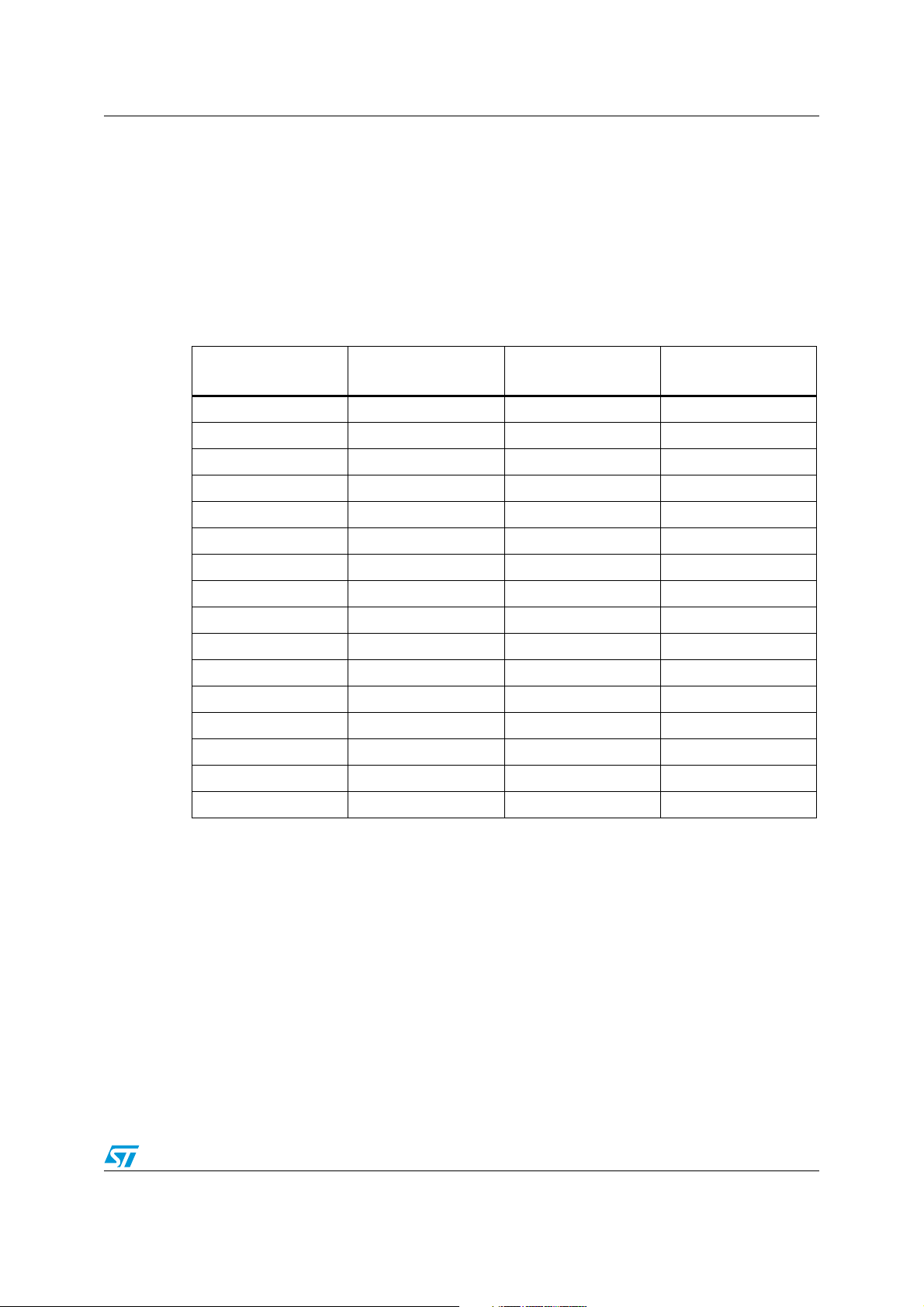
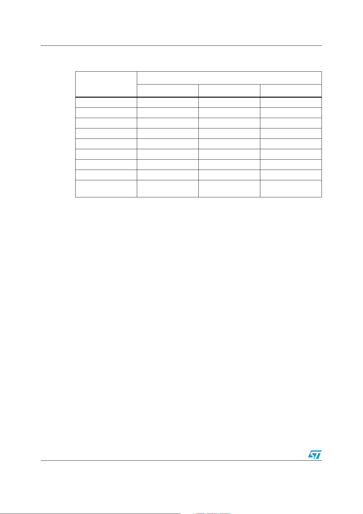
Table 2. STM32F30x family device features and peripheral counts
Peripheral
STM32F
302Cx
STM32F
302Rx
STM32F
302Vx
STM32F
303Cx
STM32F
303Rx
STM32F
303Vx
Flash (Kbytes) 128 256 128 256 128 256 128 256 128 256 128 256
SRAM (Kbytes) on
data bus
24 32 24 32 24 32 32 40 32 40 32 40
SRAM (Kbytes) on
instruction bus (CCM:
8
core coupled memory)
Timers
Advanced
control
General
purpose
1 (16-bit) 2 (16-bit)
5 (16-bit)
1 (32 bit)
Basic 1 (16-bit) 2 (16-bit)
Comm.
interfaces
SPI(I2S)
2
I
(1)
C2
USART 3
UART 2
33(2)
CAN 1
USB 1
GPIOs 37 52 87 37 52 87
DMA channels 12
12-bit ADCs 2 4
12-bit DAC channels 1 2
Analog comparator 4 7
Operational amplifiers 2 4
CPU frequency 72 MHz
Operating voltage 2.0 to 3.6 V
Operating
temperature
Ambient operating temperature: - 40 to 85 °C / - 40 to 105 °C
Junction temperature: - 40 to 125 °C
Packages LQFP48 LQFP64 LQFP100 LQFP48 LQFP64 LQFP100
1. In 128K and 256K Flash STM32F303xx devices the SPI interfaces can work in an exclusive way in either the SPI mode or
the I2S audio mode.
Doc ID 023353 Rev 1 9/119
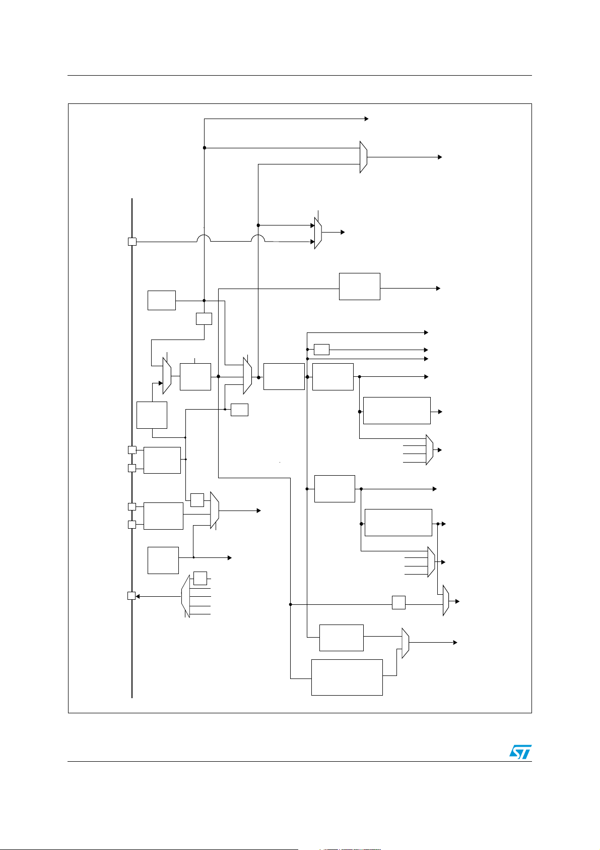
Device overview STM32F302xx/STM32F303xx
MS18959V5
Touch Sensing
Controller
AHB decoder
TIMER 16
2 Channels,1 Comp
Channel, BRK as AF
TIMER 17
TIMER 1 / PWM
SPI1
MOSI, MISO,
SCK,NSS as AF
USART1
RX, TX, CTS, RTS,
SmartCard as AF
WinWATCHDOG
BusMatrix
MPU/FPU
Cortex M4 CPU
F
max
: 72 MHz
NVIC
GP DMA1
7 channels
CCM RAM
8KB
Flash
interface
OBL
FLASH 256 KB
64 bits
JTRST
JTDI
JTCK/SWCLK
JTMS/SWDAT
JTDO
As AF
Power
Voltage reg.
3.3 V to 1.8V
V
DD18
Supply
Supervision
POR /PDR
PVD
POR
Reset
Int.
V
DDIO
= 2 to 3.6 V
V
SS
NRESET
V
DDA
V
SSA
Ind. WDG32K
Standby
interface
PLL
@V
DDIO
@V
DDA
XTAL OSC
4 -32 MHz
Reset &
clock
control
AHBPCLK
APBP1CLK
APBP2CLK
AHB2
APB2
AHB2
APB1
CRC
APB1 F
max
= 36 MHz
APB2 f
max
= 72 MHz
GPIO PORT A
GPIO PORT B
GPIO PORT C
GPIO PORT D
GPIO PORT E
OSC_IN
OSC_OUT
SPI3
SCL, SDA, SMBAL as AF
USART2
SCL, SDA, SMBAL as AF
USART3
RC LS
TIMER6
TIMER 4
SPI2
12bit DAC1IF
@V
DDA
TIMER2
(32-bit/PWM)
PA[15:0]
PB[15:0]
PC[15:0]
MOSI, MISO,
SCK, NSS as AF
4 Channels, ETR as AF
USBDP, USBDM
DAC1_CH1 as AF
HCLK
FCLK
USARTCLK
RC HS 8MHz
SRAM
40 KB
ETM
Trace/Trig
SWJTAG
TPIU
Ibus
TRADECLK
TRACED[0-3]
as AF
Dbus
System
GP DMA2
5 channels
12-bit ADC1
12-bit ADC2
Temp. sensor
V
REF+
V
REF-
TIMER 15
EXT.IT
WKUP
XX AF
1 Channel, 1 Comp
Channel, BRK as AF
1 Channel, 1 Comp
Channel, BRK as AF
4 Channels,
4 Comp channels,
ETR, BRK as AF
GPIO PORT F
PD[15:0]
PE[15:0]
USB SRAM 512B
PF[7:0]
IF
I2CCLK
ADC SAR
1/2/3/4 CLK
@V
DDIO
@V
DDA
@VSW
XTAL 32kHz
OSC32_IN
OSC32_OUT
V
BAT
= 1.65V to 3.6V
RTC
AWU
Backup
Reg
(64Byte)
Backup
interface
ANTI-TAMP
TIMER 3
UART4
UART5
I2C1
I2C2
bx CAN &
512B SRAM
USB 2.0 FS
OpAmp1
OpAmp2
@V
DDA
INxx / OUTxx
INxx / OUTxx
INTERFACE
SYSCFG CTL
GP Comparator 6
GP Comparator 4
GP Comparator 2
CAN TX, CAN RX
4 Channels, ETR as AF
4 Channels, ETR as AF
RX, TX, CTS, RTS, as AF
RX, TX, CTS, RTS, as AF
RX, TX as AF
RX, TX as AF
@V
DDA
Xx Ins, 4 OUTs as AF
XX Groups of
4 channels as AF
MOSI, MISO,
SCK, NSS as AF
GP Comparator 1
2 Device overview
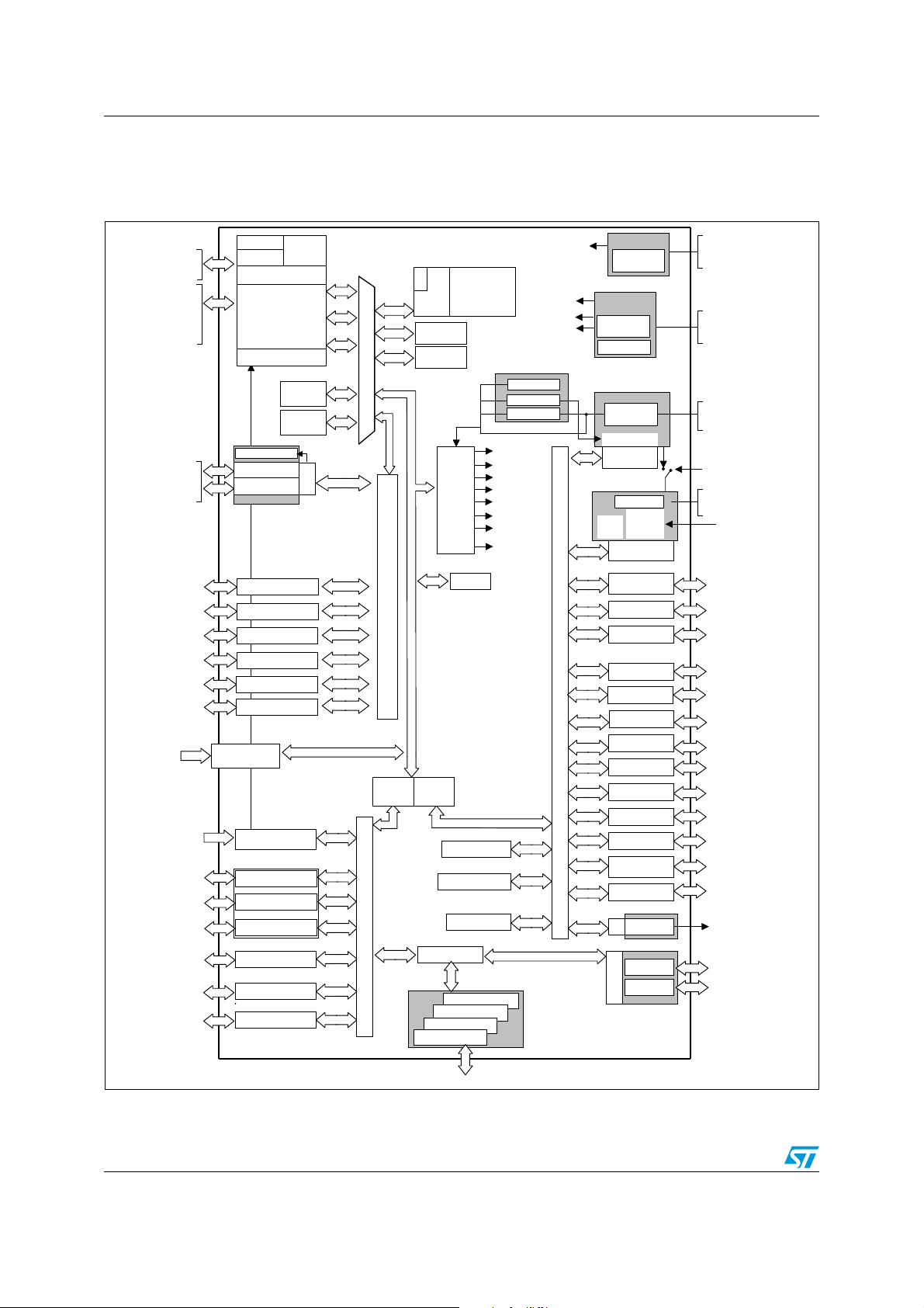
Figure 1. STM32F302xx block diagram
1. AF: alternate function on I/O pins.
10/119 Doc ID 023353 Rev 1
STM32F302xx/STM32F303xx Device overview
MS18960V4
Touch Sensing
Controller
AHB decoder
TIMER 16
2 Channels,1 Comp
Channel, BRK as AF
TIMER 17
TIMER 1 / PWM
TIMER 8 / PWM
4 Channels,
4 Comp channels,
ETR, BRK as AF
SPI1
MOSI, MISO,
SCK,NSS as AF
USART1
RX, TX, CTS, RTS,
SmartCard as AF
WinWATCHDOG
BusMatrix
MPU/FPU
Cortex M4 CPU
F
max
: 72 MHz
NVIC
GP DMA1
7 channels
CCM RAM
8KB
Flash
interface
OBL
FLASH 256 KB
64 bits
JTRST
JTDI
JTCK/SWCLK
JTMS/SWDAT
JTDO
As AF
Power
Voltage reg.
3.3 V to 1.8V
V
DD18
Supply
Supervision
POR /PDR
PVD
POR
Reset
Int.
V
DDIO
= 2 to 3.6 V
V
SS
NRESET
V
DDA
V
SSA
Ind. WDG32K
Standby
interface
PLL
@V
DDIO
@V
DDA
XTAL OSC
4 -32 MHz
Reset &
clock
control
AHBPCLK
APBP1CLK
APBP2CLK
AHB2
APB2
AHB2
APB1
CRC
APB1 F
max
= 36 MHz
APB2 f
max
= 72 MHz
GPIO PORT A
GPIO PORT B
GPIO PORT C
GPIO PORT D
GPIO PORT E
OSC_IN
OSC_OUT
SPI3/I2S
SCL, SDA, SMBAL as AF
USART2
SCL, SDA, SMBAL as AF
USART3
RC LS
TIMER6
TIMER 4
SPI2/I2S
12bit DAC1IF
@V
DDA
TIMER2
(32-bit/PWM)
PA[15:0]
PB[15:0]
PC[15:0]
MOSI/SD, MISO/ext_SD,
SCK/CK, NSS/WS, MCLK as AF
4 Channels, ETR as AF
USBDP, USBDM
DAC1_CH1 as AF
HCLK
FCLK
USARTCLK
RC HS 8MHz
SRAM
40 KB
ETM
Trace/Trig
SWJTAG
TPIU
Ibus
TRADECLK
TRACED[0-3]
as AF
Dbus
System
GP DMA2
5 channels
12-bit ADC1
12-bit ADC2
IF
Temp. sensor
V
REF+
V
REF-
TIMER 15
EXT.IT
WKUP
XX AF
1 Channel, 1 Comp
Channel, BRK as AF
1 Channel, 1 Comp
Channel, BRK as AF
4 Channels,
4 Comp channels,
ETR, BRK as AF
GPIO PORT F
PD[15:0]
PE[15:0]
TIMER7
USB SRAM 512B
PF[7:0]
12-bit ADC3
IF
12-bit ADC4
I2CCLK
ADC SAR
1/2/3/4 CLK
@V
DDIO
@V
DDA
@VSW
XTAL 32kHz
OSC32_IN
OSC32_OUT
V
BAT
= 1.65V to 3.6V
RTC
AWU
Backup
Reg
(64Byte)
Backup
interface
ANTI-TAMP
TIMER 3
UART4
UART5
I2C1
I2C2
bx CAN &
512B SRAM
USB 2.0 FS
DAC1_CH2 as AF
OpAmp1
OpAmp2
OpAmp3
OpAmp4
@V
DDA
INxx / OUTxx
INxx / OUTxx
INxx / OUTxx
INxx / OUTxx
INTERFACE
SYSCFG CTL
GP Comparator 7
p
GP Comparator...
GP Comparator 1
CAN TX, CAN RX
4 Channels, ETR as AF
4 Channels, ETR as AF
MOSI/SD, MISO/ext_SD,
SCK/CK, NSS/WS, MCLK as AF
RX, TX, CTS, RTS, as AF
RX, TX, CTS, RTS, as AF
RX, TX as AF
RX, TX as AF
@V
DDA
Xx Ins, 7 OUTs as AF
XX Groups of
4 channels as AF
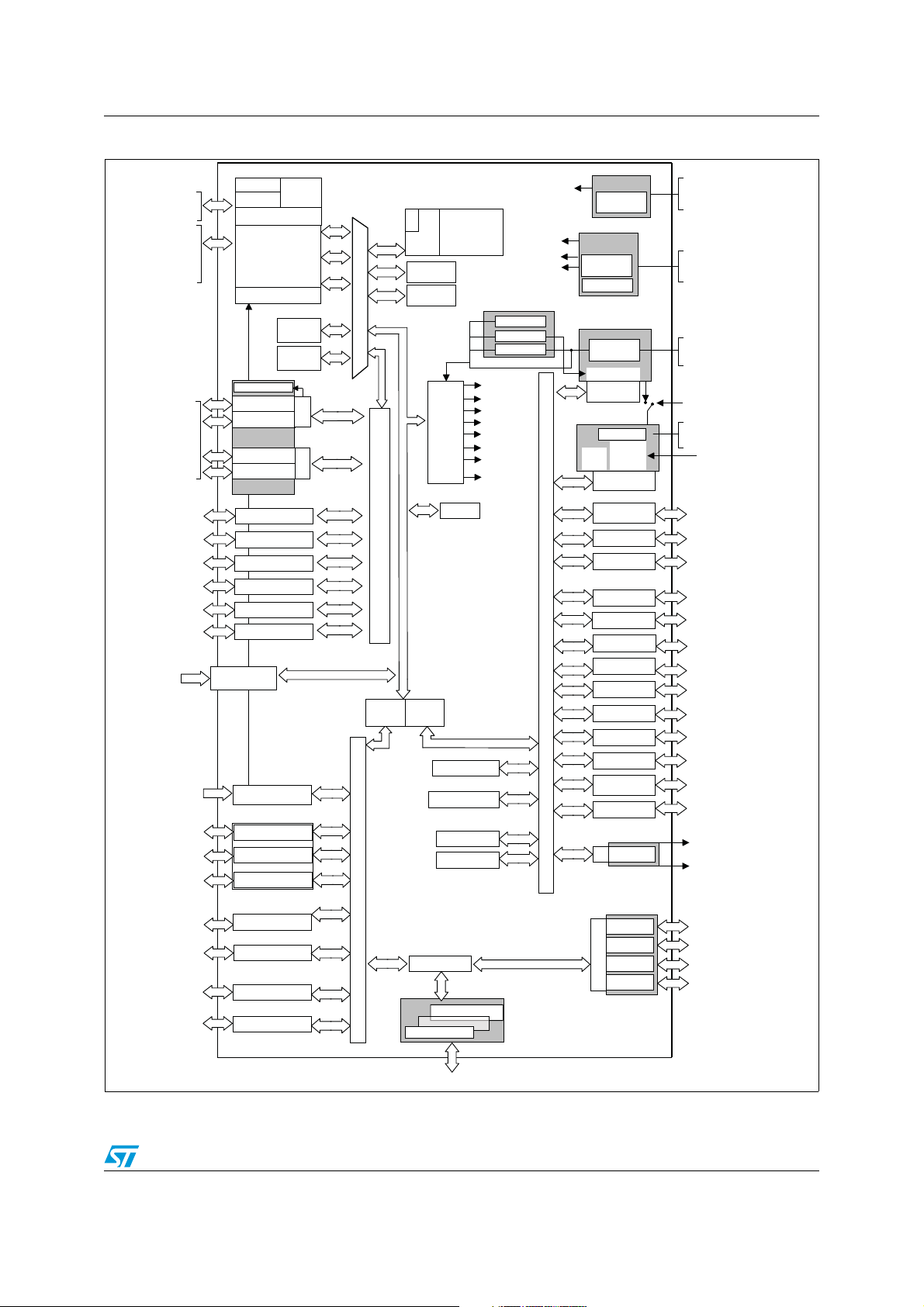
Figure 2. STM32F303xx block diagram
1. AF: alternate function on I/O pins.
Doc ID 023353 Rev 1 11/119
Device overview STM32F302xx/STM32F303xx
Figure 3. Clock tree
FLITFCLK
to Flash programming interface
HSI
to I2Cx (x = 1,2)
I2S_CKIN
SYSCLK
Ext. clock
I2SSRC
SYSCLK
to I2Sx (x = 2,3)
OSC_OUT
OSC_IN
OSC32_IN
OSC32_OUT
MCO
8 MHz
HSI RC
PLLSRC
/2,/3,...
/16
4-32 MHz
HSE OSC
LSE OSC
32.768kHz
LSI RC
40kHz
Main clock
output
HSI
PLLMUL
PLL
x2,x3,..
x16
/32
LSE
MCO
/2
HSI
PLLCLK
HSE
CSS
RTCCLK
RTCSEL[1:0]
LSI
/2
to IWWDG
IWWDGCLK
PLLCLK
HSI
LSI
HSE
SYSCLK
SW
AHB
AHB
prescaler
/1,2,..512
SYSCLK
to RTC
USB
prescaler
/1,1.5
HCLK
/8
APB1
prescaler
/1,2,4,8,16
APB2
prescaler
/1,2,4,8,16
ADC
Prescaler
/1,2,4
Prescaler
/1,2,4,6,8,10,12,16,
32,64,128,256
PCLK1
If (APB1 prescaler
=1) x1 else x2
SYSCLK
PCLK2
If (APB2 prescaler
=1) x1 else x2
SYSCLK
ADC
PCLK1
HSI
LSE
PCLK2
HSI
LSE
x2
USBCLK
to USB interface
to AHB bus, core,
memory and DMA
to cortex System timer
FHCLK Cortex free
running clock
to APB1 peripherals
to TIM 2,3,4,6,7
to USARTx (x = 2..5)
to APB2 peripherals
to TIM 15,16,17
to USART1
TIM1/8
to ADCxy
(xy = 12, 34)
MS19989V2
12/119 Doc ID 023353 Rev 1

STM32F302xx/STM32F303xx Functional overview
3 Functional overview
3.1 ARM® Cortex™-M4 core with embedded Flash and SRAM
The ARM Cortex-M4 processor is the latest generation of ARM processors for embedded
systems. It was developed to provide a low-cost platform that meets the needs of MCU
implementation, with a reduced pin count and low-power consumption, while delivering
outstanding computational performance and an advanced response to interrupts.
The ARM Cortex-M4 32-bit RISC processor features exceptional code-efficiency, delivering
the high-performance expected from an ARM core in the memory size usually associated
with 8- and 16-bit devices.
The processor supports a set of DSP instructions which allow efficient signal processing
and complex algorithm execution.
Its single precision FPU speeds up software development by using metalanguage
development tools, while avoiding saturation.
With its embedded ARM core, the STM32F302xx/STM32F303xx family is compatible with
all ARM tools and software.
Figure 1 and Figure 2 show the general block diagrams of the
STM32F302xx/STM32F303xx family devices.
3.2 Memory protection unit
The memory protection unit (MPU) is used to separate the processing of tasks from the data
protection. The MPU can manage up to 8 protection areas that can all be further divided up
into 8 subareas. The protection area sizes are between 32 bytes and the whole 4 gigabytes
of addressable memory.
The memory protection unit is especially helpful for applications where some critical or
certified code has to be protected against the misbehavior of other tasks. It is usually
managed by an RTOS (real-time operating system). If a program accesses a memory
location that is prohibited by the MPU, the RTOS can detect it and take action. In an RTOS
environment, the kernel can dynamically update the MPU area setting, based on the
process to be executed.
The MPU is optional and can be bypassed for applications that do not need it.
The Cortex-M4 processor is a high performance 32-bit processor designed for the
microcontroller market. It offers significant benefits to developers, including:
● Outstanding processing performance combined with fast interrupt handling
● Enhanced system debug with extensive breakpoint and trace capabilities
● Efficient processor core, system and memories
● Ultralow power consumption with integrated sleep modes
● Platform security robustness with optional integrated memory protection unit (MPU)
With its embedded ARM core, the STM32F302xx/STM32F303xx devices are compatible
with all ARM development tools and software.
Doc ID 023353 Rev 1 13/119

Functional overview STM32F302xx/STM32F303xx
3.3 Nested vectored interrupt controller (NVIC)
The STM32F302xx/STM32F303xx devices embed a nested vectored interrupt controller
(NVIC) able to handle up to 66 maskable interrupt channels and 16 priority levels.
The NVIC benefits are the following:
● Closely coupled NVIC gives low latency interrupt processing
● Interrupt entry vector table address passed directly to the core
● Closely coupled NVIC core interface
● Allows early processing of interrupts
● Processing of late arriving higher priority interrupts
● Support for tail chaining
● Processor state automatically saved
● Interrupt entry restored on interrupt exit with no instruction overhead
The NVIC hardware block provides flexible interrupt management features with minimal
interrupt latency.
3.4 Embedded Flash memory
All STM32F302xx/STM32F303xx devices feature up to 256 Kbytes of embedded Flash
memory available for storing programs and data. The Flash memory access time is adjusted
to the CPU clock frequency (0 wait state from 0 to 24 MHz, 1 wait state from 24 to 48 MHz
and 2 wait states above).
3.5 CRC (cyclic redundancy check) calculation unit
The CRC (cyclic redundancy check) calculation unit is used to get a CRC code using a
configurable generator polynomial value and size.
Among other applications, CRC-based techniques are used to verify data transmission or
storage integrity. In the scope of the EN/IEC 60335-1 standard, they offer a means of
verifying the Flash memory integrity. The CRC calculation unit helps compute a signature of
the software during runtime, to be compared with a reference signature generated at
linktime and stored at a given memory location.
3.6 Embedded SRAM
STM32F302xx/STM32F303xx devices feature up to 48 Kbytes of embedded SRAM with
hardware parity check. The memory can be accessed in read/write at CPU clock speed with
0 wait states, allowing the CPU to achieve 90 Dhrystone Mips at 72 MHz (when running
code from CCM, core coupled memory).
● 8 Kbytes of SRAM mapped on the instruction bus (Core Coupled Memory (CCM)),
used to execute critical routines or to access data (parity check on all of CCM RAM).
● 40 Kbytes of SRAM mapped on the data bus (parity check on first 16 Kbytes of SRAM)
14/119 Doc ID 023353 Rev 1

STM32F302xx/STM32F303xx Functional overview
3.7 Clocks and startup
System clock selection is performed on startup, however the internal RC 8 MHz oscillator is
selected as default CPU clock on reset. An external 4-32 MHz clock can be selected, in
which case it is monitored for failure. If failure is detected, the system automatically switches
back to the internal RC oscillator. A software interrupt is generated if enabled. Similarly, full
interrupt management of the PLL clock entry is available when necessary (for example with
failure of an indirectly used external oscillator).
Several prescalers allow to configure the AHB frequency, the high speed APB (APB2) and
the low speed APB (APB1) domains. The maximum frequency of the AHB and the high
speed APB domains is 72 MHz, while the maximum allowed frequency of the low speed
APB domain is 36 MHz.
3.8 Boot modes
At startup, Boot0 pin and Boot1 option bit are used to select one of three boot options:
● Boot from user Flash
● Boot from system memory
● Boot from embedded SRAM
The boot loader is located in system memory. It is used to reprogram the Flash memory by
using USART1 or USART2 or USB(DFU).
3.9 Power supply schemes
● V
SS
provided externally through V
● V
SSA
operational amplifiers, reset blocks, RCs and PLL (minimum voltage to be applied to
V
DDA
level must be always greater or equal to the V
first.
● V
BAT
registers (through power switch) when V
=
, V
2.0 to 3.6 V: external power supply for I/Os and the internal regulator. It is
DD
DD
, V
= 2.0 to 3.6 V: external analog power supply for ADC, DACs, comparators
DDA
is 2.4 V when the DACs and operational amplifiers are used). The V
= 1.65 to 3.6 V: power supply for RTC, external clock 32 kHz oscillator and backup
3.10 Power supply supervisor
The device has an integrated power-on reset (POR) and power-down reset (PDR) circuits.
They are always active, and ensure proper operation above a threshold of 2 V. The device
remains in reset mode when the monitored supply voltage
V
POR/PDR, without the need for an external reset circuit.
● The POR monitors only the V
that V
● The PDR monitors both the V
should arrive first and be greater than or equal to VDD.
DDA
supply supervisor can be disabled (by programming a dedicated Option bit) to reduce
the power consumption if the application design ensures that V
equal to V
DD
.
DD
DD
pins.
voltage
voltage level and must be provided
DD
is not present.
DD
is below a specified threshold,
DDA
supply voltage. During the startup phase it is required
and V
supply voltages, however the V
DDA
DDA
power
DDA
is higher than or
Doc ID 023353 Rev 1 15/119

Functional overview STM32F302xx/STM32F303xx
The device features an embedded programmable voltage detector (PVD) that monitors the
V
power supply and compares it to the VPVD threshold. An interrupt can be generated
DD
when V
drops below the V
DD
threshold and/or when V
PVD
is higher than the V
DD
PVD
threshold. The interrupt service routine can then generate a warning message and/or put
the MCU into a safe state. The PVD is enabled by software.
3.11 Voltage regulator
The regulator has three operation modes: main (MR), low power (LPR), and power-down.
● The MR mode is used in the nominal regulation mode (Run)
● The LPR mode is used in Stop mode.
● The power-down mode is used in Standby mode: the regulator output is in high
impedance, and the kernel circuitry is powered down thus inducing zero consumption.
The voltage regulator is always enabled after reset. It is disabled in Standby mode.
3.12 Low-power modes
The STM32F302xx/STM32F303xx supports three low-power modes to achieve the best
compromise between low power consumption, short startup time and available wakeup
sources:
● Sleep mode
In Sleep mode, only the CPU is stopped. All peripherals continue to operate and can
wake up the CPU when an interrupt/event occurs.
● Stop mode
Stop mode achieves the lowest power consumption while retaining the content of
SRAM and registers. All clocks in the 1.8 V domain are stopped, the PLL, the HSI RC
and the HSE crystal oscillators are disabled. The voltage regulator can also be put
either in normal or in low-power mode.
The device can be woken up from Stop mode by any of the EXTI line. The EXTI line
source can be one of the 16 external lines, the PVD output, the USB wakeup on
STM32F303xx devices, the RTC alarm, COMPx, I2Cx or U(S)ARTx.
● Standby mode
The Standby mode is used to achieve the lowest power consumption. The internal
voltage regulator is switched off so that the entire 1.8 V domain is powered off. The
PLL, the HSI RC and the HSE crystal oscillators are also switched off. After entering
Standby mode, SRAM and register contents are lost except for registers in the Backup
domain and Standby circuitry.
The device exits Standby mode when an external reset (NRST pin), an IWDG reset, a
rising edge on the WKUP pin, or an RTC alarm occurs.
Note: The RTC, the IWDG, and the corresponding clock sources are not stopped by entering Stop
or Standby mode.
16/119 Doc ID 023353 Rev 1

STM32F302xx/STM32F303xx Functional overview
3.13 Real-time clock (RTC) and backup registers
The RTC and the 16 backup registers are supplied through a switch that takes power from
either the V
registers used to store 64 bytes of user application data when V
They are not reset by a system or power reset, or when the device wakes up from Standby
mode.
The RTC is an independent BCD timer/counter. It supports the following features:
● Calendar with subsecond, seconds, minutes, hours (12 or 24 format), week day, date,
month, year, in BCD (binary-coded decimal) format.
● Automatic correction for 28, 29 (leap year), 30, and 31 days of the month.
● Two programmable alarms with wake up from Stop and Standby mode capability.
● On-the-fly correction from 1 to 32767 RTC clock pulses. This can be used to
synbchronize it with a master clock.
● Digital calibration circuit with 1 ppm resolution, to compensate for quartz crystal
inaccuracy.
● Three anti-tamper detection pins with programmable filter. The MCU can be woken up
from Stop and Standby modes on tamper event detection.
● Timestamp feature which can be used to save the calendar content. This function can
be triggered by an event on the timestamp pin, or by a tamper event. The MCU can be
woken up from Stop and Standby modes on timestamp event detection.
● 17-bit Auto-reload counter for periodic interrupt with wakeup from STOP/STANDBY
capability.
supply when present or the V
DD
pin. The backup registers are sixteen 32-bit
BAT
power is not present.
DD
The RTC clock sources can be:
● A 32.768 kHz external crystal
● A resonator or oscillator
● The internal low-power RC oscillator (typical frequency of 40 kHz)
● The high-speed external clock divided by 32.
3.14 DMA (direct memory access)
The flexible general-purpose DMA is able to manage memory-to-memory, peripheral-tomemory and memory-to-peripheral transfers. The DMA controller supports circular buffer
management, avoiding the generation of interrupts when the controller reaches the end of
the buffer.
Each of the 12 DMA channels is connected to dedicated hardware DMA requests, with
software trigger support for each channel. Configuration is done by software and transfer
sizes between source and destination are independent.
The DMA can be used with the main peripherals: SPI, I
2
C, USART, general-purpose timers,
DAC and ADC.
3.15 GPIOs (general-purpose inputs/outputs)
Each of the GPIO pins can be configured by software as output (push-pull or open-drain), as
input (with or without pull-up or pull-down) or as peripheral alternate function. Most of the
Doc ID 023353 Rev 1 17/119

Functional overview STM32F302xx/STM32F303xx
GPIO pins are shared with digital or analog alternate functions. All GPIOs are high current
capable except for analog inputs.
The I/Os alternate function configuration can be locked if needed following a specific
sequence in order to avoid spurious writing to the I/Os registers.
3.16 Fast ADC (analog-to-digital converter)
Up to four fast analog-to-digital converters 5 MSPS, with selectable resolution between 12
and 6 bit, are embedded in the STM32F302xx/STM32F303xx family devices. The ADCs
have up to 39 external channels. Some of the external channels are shared between
ADC1&2 and between ADC3&4, performing conversions in single-shot or scan modes. In
scan mode, automatic conversion is performed on a selected group of analog inputs.
The ADCs have also internal channels: Temperature sensor connected to ADC1 channel
16, V
ADCs channel 18, VOPAMP1 connected to ADC1 channel 15, VOPAMP2 connected to
ADC2 channel 17, VOPAMP3 connected to ADC3 channel 17, VOPAMP4 connected to
ADC4 channel 17).
Additional logic functions embedded in the ADC interface allow:
● Simultaneous sample and hold
● Interleaved sample and hold
● Single-shunt phase current reading techniques.
connected to ADC1 channel 17, Voltage reference V
BAT/2
connected to the 4
REFINT
The ADC can be served by the DMA controller.
An analog watchdog feature allows very precise monitoring of the converted voltage of one,
some or all selected channels. An interrupt is generated when the converted voltage is
outside the programmed thresholds.
The events generated by the general-purpose timers (TIMx) and the advanced-control
timers (TIM1 on all devices and TIM8 on STM32F303xx devices) can be internally
connected to the ADC start trigger and injection trigger, respectively, to allow the application
to synchronize A/D conversion and timers.
3.16.1 Temperature sensor
The temperature sensor (TS) generates a voltage V
temperature.
The temperature sensor is internally connected to the ADC_IN16 input channel which is
used to convert the sensor output voltage into a digital value.
The sensor provides good linearity but it has to be calibrated to obtain good overall accuracy
of the temperature measurement. As the offset of the temperature sensor varies from chip
to chip due to process variation, the uncalibrated internal temperature sensor is suitable for
applications that detect temperature changes only.
To improve the accuracy of the temperature sensor measurement, each device is
individually factory-calibrated by ST. The temperature sensor factory calibration data are
stored by ST in the system memory area, accessible in read-only mode.
that varies linearly with
SENSE
18/119 Doc ID 023353 Rev 1
STM32F302xx/STM32F303xx Functional overview
Table 3. Temperature sensor calibration values
Calibration value name Description Memory address
TS ADC raw data acquired at
TS_CAL1
TS_CAL2
temperature of 30 °C,
V
= 3.3 V
DDA
TS ADC raw data acquired at
temperature of 110 °C
V
= 3.3 V
DDA
0x1FFF F7B8 - 0x1FFF F7B9
0x1FFF F7C2 - 0x1FFF F7C3
3.16.2 Internal voltage reference (V
The internal voltage reference (V
ADC and Comparators. V
The precise voltage of V
REFINT
REFINT
is internally connected to the ADC_IN18 input channel.
REFINT
is individually measured for each part by ST during
REFINT
)
) provides a stable (bandgap) voltage output for the
production test and stored in the system memory area. It is accessible in read-only mode.
Table 4. Temperature sensor calibration values
Calibration value name Description Memory address
Raw data acquired at
3.16.3 V
VREFINT_CAL
battery voltage monitoring
BAT
temperature of 30 °C
V
= 3.3 V
DDA
This embedded hardware feature allows the application to measure the V
using the internal ADC channel ADC_IN17. As the V
and thus outside the ADC input range, the V
BAT
divider by 2. As a consequence, the converted digital value is half the V
3.16.4 OPAMP reference voltage (VOPAMP)
Every OPAMP reference voltage can be measured using a corresponding ADC internal
channel: VOPAMP1 connected to ADC1 channel 15, VOPAMP2 connected to ADC2
channel 17, VOPAMP3 connected to ADC3 channel 17, VOPAMP4 connected to ADC4
channel 17.
0x1FFF F7BA - 0x1FFF F7BB
battery voltage
voltage may be higher than V
BAT
BAT
pin is internally connected to a bridge
voltage.
BAT
DDA
,
3.17 DAC (digital-to-analog converter)
Up to two 12-bit buffered DAC channels can be used to convert digital signals into analog
voltage signal outputs. The chosen design structure is composed of integrated resistor
strings and an amplifier in inverting configuration.
Doc ID 023353 Rev 1 19/119

Functional overview STM32F302xx/STM32F303xx
This digital interface supports the following features:
● Up to two DAC output channels on STM32F303xx devices
● 8-bit or 12-bit monotonic output
● Left or right data alignment in 12-bit mode
● Synchronized update capability on STM32F303xx devices
● Noise-wave generation
● Triangular-wave generation
● Dual DAC channel independent or simultaneous conversions on STM32F303xx
devices
● DMA capability (for each channel on STM32F303xx devices)
● External triggers for conversion
3.18 Operational amplifier
The STM32F302xx/STM32F303xx embeds up to four operational amplifiers with external or
internal follower routing and PGA capability (or even amplifier and filter capability with
external components). When an operational amplifier is selected, an external ADC channel
is used to enable output measurement.
The operational amplifier features:
● 8MHz GBP
● 0.5 mA output capability
● Rail-to-rail input/output
● In PGA mode, the gain can be programmed to be 2, 4, 8 or 16.
3.19 Fast comparators
The STM32F302xx/STM32F303xx devices embed seven fast rail-to-rail comparators with
programmable reference voltage (internal or external), hysteresis and speed (low speed for
low power) and with selectable output polarity.
The reference voltage can be one of the following:
● External I/O
● DAC output pin
● Internal reference voltage or submultiple (1/4, 1/2, 3/4). Refer to Table 20: Embedded
internal reference voltage on page 57 for the value and precision of the internal
reference voltage.
All comparators can wake up from STOP mode, generate interrupts and breaks for the
timers and can be also combined per pair into a window comparator
3.20 Timers and watchdogs
The STM32F302xx/STM32F303xx includes up to two advanced control timers, up to 6
general-purpose timers, two basic timers, two watchdog timers and a SysTick timer. The
table below compares the features of the advanced control, general purpose and basic
timers.
20/119 Doc ID 023353 Rev 1

STM32F302xx/STM32F303xx Functional overview
Table 5. Timer feature comparison
Timer type Timer
Counter
resolution
TIM1,
TIM8
Advanced
(on
16-bit
STM32F303xx
devices only)
General-
purpose
General-
purpose
General-
purpose
General-
purpose
TIM2 32-bit
TIM3, TIM4 16-bit
TIM15 16-bit Up
TIM16, TIM17 16-bit Up
TIM6,
TIM7
Basic
(on
16-bit Up
STM32F303xx
devices only)
Counter
type
Up, Down,
Up/Down
Up, Down,
Up/Down
Up, Down,
Up/Down
Prescaler
factor
Any integer
between 1
and 65536
Any integer
between 1
and 65536
Any integer
between 1
and 65536
Any integer
between 1
and 65536
Any integer
between 1
and 65536
Any integer
between 1
and 65536
DMA
request
generation
Capture/
compare
Channels
Complementary
Ye s 4 Ye s
Ye s 4 N o
Ye s 4 N o
Ye s 2 1
Ye s 1 1
Ye s 0 N o
outputs
3.20.1 Advanced timers (TIM1, TIM8)
The advanced-control timers (TIM1 on all devices and TIM8 on STM32F303xx devices) can
each be seen as a three-phase PWM multiplexed on 6 channels. They have complementary
PWM outputs with programmable inserted dead-times. They can also be seen as complete
general-purpose timers. The 4 independent channels can be used for:
● Input capture
● Output compare
● PWM generation (edge or center-aligned modes) with full modulation capability (0-
100%)
● One-pulse mode output
In debug mode, the advanced-control timer counter can be frozen and the PWM outputs
disabled to turn off any power switches driven by these outputs.
Many features are shared with those of the general-purpose TIM timers (described in
Section 3.20.2 using the same architecture, so the advanced-control timers can work
together with the TIM timers via the Timer Link feature for synchronization or event chaining.
Doc ID 023353 Rev 1 21/119

Functional overview STM32F302xx/STM32F303xx
3.20.2 General-purpose timers (TIM2, TIM3, TIM4, TIM15, TIM16, TIM17)
There are up to six synchronizable general-purpose timers embedded in the
STM32F302xx/STM32F303xx (see Tab l e 5 for differences). Each general-purpose timer
can be used to generate PWM outputs, or act as a simple time base.
● TIM2, 3, and TIM4
These are full-featured general-purpose timers:
– TIM2 has a 32-bit auto-reload up/downcounter and 32-bit prescaler
– TIM3 and 4 have 16-bit auto-reload up/downcounters and 16-bit prescalers.
These timers all feature 4 independent channels for input capture/output compare,
PWM or one-pulse mode output. They can work together, or with the other generalpurpose timers via the Timer Link feature for synchronization or event chaining.
The counters can be frozen in debug mode.
All have independent DMA request generation and support quadrature encoders.
● TIM15, 16 and 17
These three timers general-purpose timers with mid-range features:
They have 16-bit auto-reload upcounters and 16-bit prescalers.
– TIM15 has 2 channels and 1 complementary channel
– TIM16 and TIM17 have 1 channel and 1 complementary channel
All channels can be used for input capture/output compare, PWM or one-pulse mode
output.
The timers can work together via the Timer Link feature for synchronization or event
chaining. The timers have independent DMA request generation.
The counters can be frozen in debug mode.
3.20.3 Basic timers (TIM6, TIM7)
These timers are mainly used for DAC trigger generation. They can also be used as a
generic16-bit time base.
3.20.4 Independent watchdog
The independent watchdog is based on a 12-bit downcounter and 8-bit prescaler. It is
clocked from an independent 40 kHz internal RC and as it operates independently from the
main clock, it can operate in Stop and Standby modes. It can be used either as a watchdog
to reset the device when a problem occurs, or as a free running timer for application timeout
management. It is hardware or software configurable through the option bytes. The counter
can be frozen in debug mode.
3.20.5 Window watchdog
The window watchdog is based on a 7-bit downcounter that can be set as free running. It
can be used as a watchdog to reset the device when a problem occurs. It is clocked from the
main clock. It has an early warning interrupt capability and the counter can be frozen in
debug mode.
22/119 Doc ID 023353 Rev 1
STM32F302xx/STM32F303xx Functional overview
3.20.6 SysTick timer
This timer is dedicated to real-time operating systems, but could also be used as a standard
down counter. It features:
● A 24-bit down counter
● Autoreload capability
● Maskable system interrupt generation when the counter reaches 0.
● Programmable clock source
3.21 Communication interfaces
3.21.1 I2C bus
Up to two I2C bus interfaces can operate in multimaster and slave modes. They can support
standard (up to 100 KHz), fast (up to 400 KHz) and fast mode + (up to 1 MHz) modes.
Both support 7-bit and 10-bit addressing modes, multiple 7-bit slave addresses (2
addresses, 1 with configurable mask). They also include programmable analog and digital
noise filters.
Table 6. Comparison of I2C analog and digital filters
Analog filter Digital filter
Pulse width of
suppressed spikes
Benefits Available in Stop mode
Drawbacks
≥ 50 ns
Variations depending on
temperature, voltage, process
Programmable length from 1 to 15
I2C peripheral clocks
1. Extra filtering capability vs.
standard requirements.
2. Stable length
Disabled when Wakeup from Stop
mode is enabled
In addition, they provide hardware support for SMBUS 2.0 and PMBUS 1.1: ARP capability,
Host notify protocol, hardware CRC (PEC) generation/verification, timeouts verifications and
ALERT protocol management. They also have a clock domain independent from the CPU
clock, allowing the I2Cx (x=1,2) to wake up the MCU from Stop mode on address match.
The I2C interfaces can be served by the DMA controller.
3.21.2 Universal synchronous/asynchronous receiver transmitter (USART)
The STM32F302xx/STM32F303xx devices have three embedded universal
synchronous/asynchronous receiver transmitters (USART1, USART2 and USART3).
The USART interfaces are able to communicate at speeds of up to 9Mbits/s.
They provide hardware management of the CTS and RTS signals, they support IrDA SIR
ENDEC, the multiprocessor communication mode, the single-wire half-duplex
communication mode and have LIN Master/Slave capability. The USART interfaces can be
served by the DMA controller.
Doc ID 023353 Rev 1 23/119

Functional overview STM32F302xx/STM32F303xx
3.21.3 Universal asynchronous receiver transmitter (UART)
The STM32F302xx/STM32F303xx devices have 2 embedded universal asynchronous
receiver transmitters (UART4, and UART5). The UART interfaces support IrDA SIR
ENDEC, multiprocessor communication mode and single-wire half-duplex communication
mode. The UART interfaces can be served by the DMA controller.
3.21.4 Serial peripheral interface (SPI)/Inter-integrated sound interfaces
2
(I
S)
Up to three SPIs are able to communicate up to 18 Mbits/s in slave and master modes in
full-duplex and simplex communication modes. The 3-bit prescaler gives 8 master mode
frequencies and the frame size is configurable from 4 bits to 16 bits.
Two standard I2S interfaces (multiplexed with SPI2 and SPI3) supporting four different audio
standards can operate as master or slave at simplex and full duplex communication modes.
They can be configured to transfer 16 and 24 or 32 bits with 16-bit or 32-bit data resolution
and synchronized by a specific signal. Audio sampling frequency from 8 kHz up to 96 kHz
can be set by 8-bit programmable linear prescaler. When operating in master mode it can
output a clock for an external audio component at 256 times the sampling frequency.
3.21.5 Controller area network (CAN)
The CAN is compliant with specifications 2.0A and B (active) with a bit rate up to 1 Mbit/s. It
can receive and transmit standard frames with 11-bit identifiers as well as extended frames
with 29-bit identifiers. It has three transmit mailboxes, two receive FIFOs with 3 stages and
14 scalable filter banks.
3.21.6 Universal serial bus (USB)
The STM32F302xx/STM32F303xx medium and high density devices embed an USB device
peripheral compatible with the USB full-speed 12 Mbs. The USB interface implements a fullspeed (12 Mbit/s) function interface. It has software-configurable endpoint setting and
suspend/resume support. The dedicated 48 MHz clock is generated from the internal main
PLL (the clock source must use a HSE crystal oscillator).
3.22 Touch sensing controller (TSC)
The device has an embedded independent hardware controller (TSC) for controlling touch
sensing acquisitions on the I/Os.
Up to 18 touch sensing electrodes can be controlled by the TSC. The touch sensing I/Os are
organized in 8 acquisition groups, with up to 4 I/Os in each group.
The STM32F302xx/STM32F303xx devices provide a simple solution for adding capacitive
sensing functionality to any application. Capacitive sensing technology is able to detect the
presence of a finger near an electrode which is protected from direct touch by a dielectric
(glass, plastic, ...). The capacitive variation introduced by the finger (or any conductive
object) is measured using a proven implementation based on a surface charge transfer
acquisition principle. It consists of charging the electrode capacitance and then transferring
a part of the accumulated charges into a sampling capacitor until the voltage across this
capacitor has reached a specific threshold. To limit the CPU bandwidth usage this
24/119 Doc ID 023353 Rev 1
STM32F302xx/STM32F303xx Functional overview
acquisition is directly managed by the hardware touch sensing controller and only requires
few external components to operate. The STM32F302xx/STM32F303xx devices offer up to
24 capacitive sensing channels distributed over 8 analog I/O groups.
The touch sensing controller is fully supported by the STMTouch touch sensing firmware
library which is free to use and allows touch sensing functionality to be implemented reliably
in the end application.
Table 7. Capacitive sensing GPIOs available on STM32F302xx/STM32F303xx
devices
Pin name
PA0 G1_IO1 PB3 G5_IO1
PA1 G1_IO2 PB4 G5_IO2
PA2 G1_IO3 PB6 G5_IO3
PA3 G1_IO4 PB7 G5_IO4
PA4 G2_IO1 PB11 G6_IO1
PA5 G2_IO2 PB12 G6_IO2
PA6 G2_IO3 PB13 G6_IO3
PA7 G2_IO4 PB14 G6_IO4
PC5 G3_IO1 PE2 G7_IO1
PB0 G3_IO2 PE3 G7_IO2
PB1 G3_IO3 PE4 G7_IO3
PB2 G3_IO4 PE5 G7_IO4
PA9 G4_IO1 PD12 G8_IO1
PA10 G4_IO2 PD13 G8_IO2
PA13 G4_IO3 PD14 G8_IO3
PA14 G4_IO4 PD15 G8_IO4
Capacitive sensing
group name
Pin name
Capacitive sensing
group name
Doc ID 023353 Rev 1 25/119
Functional overview STM32F302xx/STM32F303xx
Table 8. No. of capacitive sensing channels available on
STM32F302xx/STM32F303xx devices
Number of capacitive sensing channels
Analog I/O group
STM32F30xVx STM32F30xRx STM32F30xCx
G1 3 3 3
G2 3 3 3
G3 3 3 2
G4 3 3 3
G5 3 3 3
G6 3 3 3
G7 3 0 0
G8 3 0 0
Number of capacitive
sensing channels
24 18 17
3.23 Development support
3.23.1 Serial wire JTAG debug port (SWJ-DP)
The ARM SWJ-DP Interface is embedded, and is a combined JTAG and serial wire debug
port that enables either a serial wire debug or a JTAG probe to be connected to the target.
The JTAG TMS and TCK pins are shared respectively with SWDIO and SWCLK and a
specific sequence on the TMS pin is used to switch between JTAG-DP and SW-DP.
3.23.2 Embedded trace macrocell™
The ARM embedded trace macrocell provides a greater visibility of the instruction and data
flow inside the CPU core by streaming compressed data at a very high rate from the
STM32F302xx/STM32F303xx through a small number of ETM pins to an external hardware
trace port analyzer (TPA) device. The TPA is connected to a host computer using a highspeed channel. Real-time instruction and data flow activity can be recorded and then
formatted for display on the host computer running debugger software. TPA hardware is
commercially available from common development tool vendors. It operates with third party
debugger software tools.
26/119 Doc ID 023353 Rev 1

STM32F302xx/STM32F303xx Pinouts and pin description
MS19819V2
VDD_1
VSS_1
PB9
PB8
BOOT0
PB7
PB6
PB5
PB4
PB3
PA15
PA14
48 47 46 45 44 43 42 41 40 39 38 37
VBAT
136
VDD_3
PC13
235
VSS_3
PC14 / OSC32_IN
334
PA13
PC15 OSC32_OUT
433
PA12
PF0 OSC_IN
532
PA11
PF1 OSC_OUT
6
48-pins
31
PA10
NRST
730
PA9
VSSA
829
PA8
VDDA
928
PB15
P
A
0
10 27
PB14
PA1
11 26
PB13
PA2
12 25
PB12
13 14 15 16 17 18 19 20 21 22 23 24
PA3
PA4
PA5
PA6
PA7
PB0
PB1
PB2
PB10
PB11
VSS_2
VDD_2
/
/
/
4 Pinouts and pin description
Figure 4. STM32F302xx/STM32F303xx LQFP48 pinout
Doc ID 023353 Rev 1 27/119

Pinouts and pin description STM32F302xx/STM32F303xx
ai18484V2
VDD_1
VSS_1
PB9
PB8
BOOT0
PB7
PB6
PB5
PB4
PB3
PD2
PC12
PC11
PC10
PA15
PA14
64 63 62 61 60 59 58 57 56 55 54 53 52 51 50 49
VBAT
148
VDD_3
PC13
247
VSS_3
PC14 / OSC32_IN
346
PA13
PC15 / OSC32_OUT
445
PA12
PF0 / OSC_IN
544
PA11
PF1 / OSC_OUT
643
PA10
NRST
742
PA9
PC0
8
64-pins
41
PA8
PC1
940
PC9
PC2
10 39
PC8
PC3
11 38
PC7
VSSA
12 37
PC6
VDDA
13 36
PB15
PA0
14 35
PB14
PA1
15 34
PB13
PA2
16 33
PB12
17 18 19 20 21 22 23 24 25 26 27 28 29 30 31 32
PA3
PF4
VDD_4
PA4
PA5
PA6
PA7
PC4
PC5
PB0
PB1
PB2
PB10
PB11
VSS_2
VDD_2
MS30357V1
VDD_1
VSS_1
PB9
PB8
BOOT0
PB7
PB6
PB5
PB4
PB3
PD2
PC12
PC11
PC10
PA15
PA14
64 63 62 61 60 59 58 57 56 55 54 53 52 51 50 49
VBAT
148
VDD_3
PC13
247
VSS_3
PC14 / OSC32_IN
346
PA13
PC15 / OSC32_OUT
445
PA12
PF0 / OSC_IN
544
PA11
PF1 / OSC_OUT
643
PA10
NRST
742
PA9
PC0
8
64-pins
41
PA8
PC1
940
PC9
PC2
10 39
PC8
PC3
11 38
PC7
VSSA
12 37
PC6
VDDA
13 36
PB15
PA0
14 35
PB14
PA1
15 34
PB13
PA2
16 33
PB12
17 18 19 20 21 22 23 24 25 26 27 28 29 30 31 32
PA3
PF4
VDD_4
PA4
PA5
PA6
PA7
PC4
PC5
PB0
PB1
NPOR
PB10
PB11
VSS_2
VDD_2
Figure 5. STM32F302xx/STM32F303xx LQFP64 pinout
28/119 Doc ID 023353 Rev 1

STM32F302xx/STM32F303xx Pinouts and pin description
AI6
6$$?
633?
0%
0%
0"
0"
"//4
0"
0"
0"
0"
0"
0$
0$
0$
0$
0$
0$
0$
0$
0#
0#
0#
0!
0!
0%
6$$?
0%
633?
0%
0&
0%
0!
0%
0!
6"!4
0!
0#
0!
0#/3#?).
0!
0#/3#?/54
0!
0&
0#
0&
0#
0&/3#?).
0#
0&/3#?/54
PINS
0#
.234
0$
0#
0$
0#
0$
0#
0$
0#
0$
0&
0$
633!
0$
6$$!
0$
62%&
0"
0"
0!
0"
0!
0"
0!
0&
6$$?
0!
0!
0!
0!
0#
0#
0"
0"
0"
0%
0%
0%
0%
0%
0%
0%
0%
0%
0"
0"
633?
6$$?
0!
Figure 6. STM32F302xx/STM32F303xx LQFP100 pinout
Doc ID 023353 Rev 1 29/119
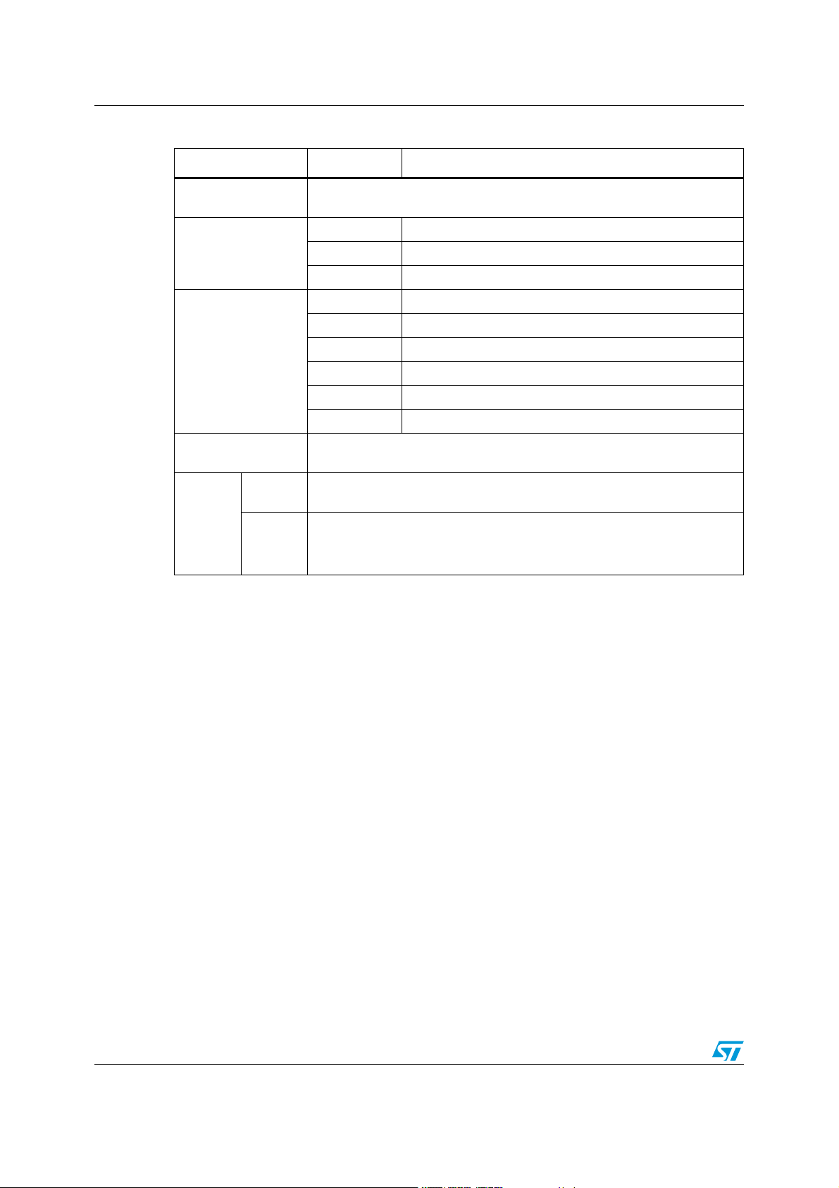
Pinouts and pin description STM32F302xx/STM32F303xx
Table 9. Legend/abbreviations used in the pinout table
Name Abbreviation Definition
Pin name
Pin type
I/O structure
Pin
functions
Notes
Alternate
functions
Additional
functions
Unless otherwise specified in brackets below the pin name, the pin function
during and after reset is the same as the actual pin name
S Supply pin
I Input only pin
I/O Input / output pin
FT 5 V tolerant I/O
FTf 5 V tolerant I/O, FM+ capable
TTa 3.3 V tolerant I/O directly connected to ADC
TC Standard 3.3V I/O
B Dedicated BOOT0 pin
RST Bidirectional reset pin with embedded weak pull-up resistor
Unless otherwise specified by a note, all I/Os are set as floating inputs during
and after reset
Functions selected through GPIOx_AFR registers
Functions directly selected/enabled through peripheral registers
30/119 Doc ID 023353 Rev 1
Loading...